[av_one_full first min_height=” vertical_alignment=” space=” custom_margin=” margin=’0px’ padding=’0px’ border=” border_color=” radius=’0px’ background_color=” src=” background_position=’top left’ background_repeat=’no-repeat’ animation=” mobile_breaking=” mobile_display=”]
[av_textblock size=” font_color=” color=” av-medium-font-size=” av-small-font-size=” av-mini-font-size=” admin_preview_bg=”]
Lab 1: An Introduction to Assembly
[/av_textblock]
[av_button label=’View Exclusively’ link=’manually,https://www.arxterra.com/ee-346-lab-1/’ link_target=” size=’medium’ position=’left’ icon_select=’yes’ icon=’ue871′ font=’entypo-fontello’ color=’dark’ custom_bg=’#444444′ custom_font=’#ffffff’ admin_preview_bg=”]
[av_textblock size=” font_color=” color=” av-medium-font-size=” av-small-font-size=” av-mini-font-size=” admin_preview_bg=”]
This lab is designed to introduce you to the Arduino Microcontroller Board, Atmel (part of MicroChip) Integrated Development Environment (IDE) and AVR Assembly Language programming. Plus, you will learn about the power of library files. Library files are simply files that you instruct AVR Studio to include in your program. In this lab you are going to include two library files. One named m328pdef and the other spi_shield.
Note: Please do the step-by-step simulation tutorial at the end of this lab. At the end of this tutorial you should be able to set switches to a given value by toggling Ports D and C pins. For example, after the tutorial you should be able to show how you would simulate an input of 0xAA.
Table of Contents
What is New?
The following instructions and assembly directives are used in Labs 1. If you have any questions on any instructions or assembly directives a nice source of information, in addition to your textbook, is the Atmel AVR Assembler User Guide
AVR Assembly Instructions
Data Transfer
in r6, PINC // Input port C pins (0x09) into register R6
out PORTB, r7 // Output to Port B from register R7
mov r8, r7 // Move data from register R7 into register R8
Arithmetic and Logic
clr r16 // Clear register R16
ser r17 // Set register R17
Control Transfer
call WriteDisplay //Subroutine Call
rjmp loop // Jump to the label named loop
AVR Studio Assembly
Directives
.INCLUDE // < > means the file is in the AVR Studio folder
.INCLUDE “spi_shield.inc” //” ” means the file is in the project folder
.CSEG // Code Segment
.ORG 0x0000 // Code Origin
Labels
loop:
Comments
; // /* */
Introduction to AVR Studio
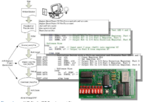
In lab you will be spending most of your time working within an IDE. For our labs we will be working in the AVR Studio IDE. As shown in the figure and discussed in the next few sections the IDE lets us write our program in a human readable form, known as assembly, and then translate it into a machine readable form understood by the ATmega328P.
Create a New Project

The best way to learn about the AVR Studio IDE is to start playing with it. So let’s get things started by launching AVR Studio and Opening a New Project.
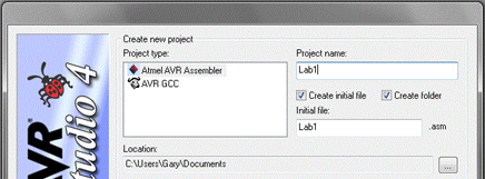
Select Atmel AVR Assembler and check both check boxes(Create initial file and Create folder). Name your project (Lab1) and browse to location where you want it saved. Click Next >>.
In the next window select AVR Simulator 2. For the Device, select ATmega328P. Click the Finish button.
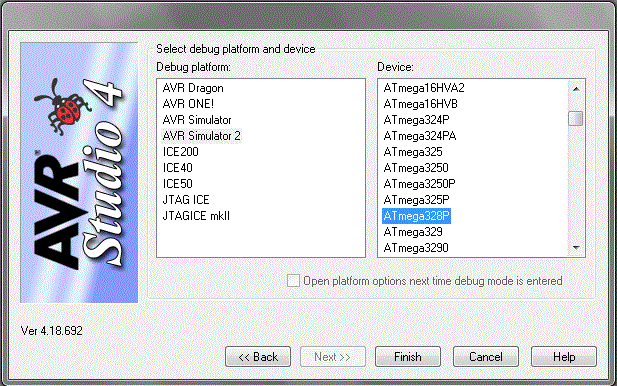
Congratulations, you are ready to start programming within the AVR Studio IDE!
Assembly Directives
All assembly programs contain assembly directives and assembly instructions. Assembly directives are instructions to be read by the assembler. In our lab, the assembler is included with AVR Studio IDE. As you have seen, AVR Studio is a program that runs on your computer and is responsible for translating your human readable assembly program into the machine language of the microcontroller.
We begin our program with an Assembly Directive. First, locate the program window within the IDE. This is the blank window in the center of your AVR Studio application. The title bar should include the location of your program and end with the name of your program and the “.asm” extension. Enter the following lines into the program window.
You can probably guess that here we are telling the assembler that we would simply like to include some comments for the individual reading our code. To include comments, you can use the C language notation // comment line and /* block comment */ or unique to assembly a semicolon ; character.
Now let’s add some code which intended strictly for the assembler, not the reader or the microcontroller. The difference is important.
.INCLUDE.CSEG .ORG 0x0000
The “dots” tell the assembler that these lines are talking to the assembler and not to be turned into machine instructions.
Without overly complicating our first program, I will just note that the INCLUDE assembly directive tells the assembler to copy into our program all the text contained in a file named m328pdef.inc. For now, we do not need to know what is in this file, other than to note it will help us in writing a more human readable program.
The CSEG statement tells the AVR Studio Assembler to place the following material in the Code SEGment of memory. For the ATmega328P, this means Flash Program Memory. The ORG statement tells the assembler to start placing code at this address in Flash Program memory.
Programming Convention Because it is so important to remember when a line is intended for the Assembler (Assembly Directive) and when a line is to be converted to a machine instruction intended for ATMega328P microcontroller (Assembly Instruction), I always capitalize Assembly Directives and place in lower case letters Assembly Instructions. AVR Studio is not case sensitive, so this convention is not required for your assembly program to assemble correctly – it is however required by the instructor.
Now let’s add our first label. Enter the following line after the .ORG 0x0000 assembly directive:
RST_VECT:
The label RST_VECT stands for ReSeT VECTor and is only there as a point of programming style (i.e., it helps the reader know that the code to be executed on reset follows). What the assembler does is quite a different story. Whenever the assembly sees a label, it places the label name and its corresponding address, in this case we know it is 0x0000, into a look-up table.
[/av_textblock]
[av_table purpose=’tabular’ pricing_table_design=’avia_pricing_default’ pricing_hidden_cells=” caption=” responsive_styling=’avia_scrollable_table’]
[av_row row_style=’avia-heading-row’][av_cell col_style=”]Label Name[/av_cell][av_cell col_style=”]Program Address[/av_cell][/av_row]
[av_row row_style=”][av_cell col_style=”]RST_VECT[/av_cell][av_cell col_style=”]0x0000[/av_cell][/av_row]
[/av_table]
[av_textblock size=” font_color=” color=” av-medium-font-size=” av-small-font-size=” av-mini-font-size=” admin_preview_bg=”]
Now if you ever want to reference this location in your program, you can use the name and let the assembler worry about the address.
Congratulations, you have for now completed your initial conversation with the assembler. You have asked it to include some comments, include more assembly directives located in another file, setup to write some code at address at 0x0000 in program memory, and finally to associate this address with the name RST_VECT. What you haven’t done is write anything that the AVR microcontroller will ever read. Once again it is important to know when you are talking to the assembler and when your code will be used to generate machine instructions to be run by the microcontroller. So let’s start generating assembly instructions intended for the microcontroller.
Assembly Instructions
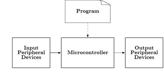
Just as you are reading the step-by-step instructions on this page so you can write your first program, the microcontroller in Figure 5 reads the step-by-step instructions contained in the program to learn what is intended by the programmer. This is the “Machine Language” of the computer. This language is comprised of only ones and zeros. For example, this binary sequence 0010011100000000 tells the AVR computer (aka microcontroller) to set all the bits in register 16 to zero. All these 0’s and 1’s are not very easy for us humans to understand. So instead we humans have created a human like language comprised of abbreviations (known as mnemonics). This is known as Assembly Language. By definition then, there is a one-to-one correspondence between a machine instruction and an assembly instruction. For our machine code example, the equivalent assembly instruction is clr r16.
Registers Our microcontroller contains 32 general purpose registers labeled R0 to R31. For now you can think of registers like variables which can hold up to 8-bits of information (000000002 = 010 to 111111112 = 25510). To learn more about number system read Chapter 1 “Introduction” in your textbook or Appendix A – Number Systems in my Lecture 1 notes.
It is finally time to write our first assembly instruction. Add the following assembly instructions to your program.
rjmp reset // jump over the IVT, tables and include file(s)
The assembly instruction rjmp Reset instructs the microcontroller to jump to the yet to be defined label named Reset. You will also see I have included a comment. The meaning of this comment will become more clear over the remainder of the semester.
The Anatomy of an Assembly Instruction
Each assembly instruction is defined by an operator and one or two operand fields. For our clr r16 example, the clear instruction’s operator is clr and it has one operand r16. Our first program line also contains a single operand instruction. In this case, the operator is rjmp and the operand is reset.
Introduction to the Arduino Proto-shield
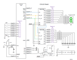
A schematic of our Arduino Proto-shield is shown in Figure 6. It includes 8 switches, 1 push button, 10 discrete LEDs, 1 seven segment display, and 2 D flip-flops. If you were to add up all the inputs and outputs required to support this proto-shield you would come up with 29. The Arduino Uno board, designed with the ATmega328P microcontroller, only has 23 general purpose digital I/O pins. So how do we solve the problem? Luck for us the ATmega328P includes a Serial Peripheral Interface (SPI) subsystem which allows us to send 8-bits of data as a serial string of 1’s and 0’s. By adding two 74HC595 8-bit Serial-to-Parallel shift registers to our Proto-shield as shown in Figure 6, and using the SPI subsystem, we are able to generate 16 new outputs. We will use these outputs to drive 8 discrete LEDs and our 7-segment display.
The ATmega328P Serial Peripheral Interface
Additional information can be found in Chapter 10 of the textbook or Section 18.2 of the ATmega328 Datasheet.
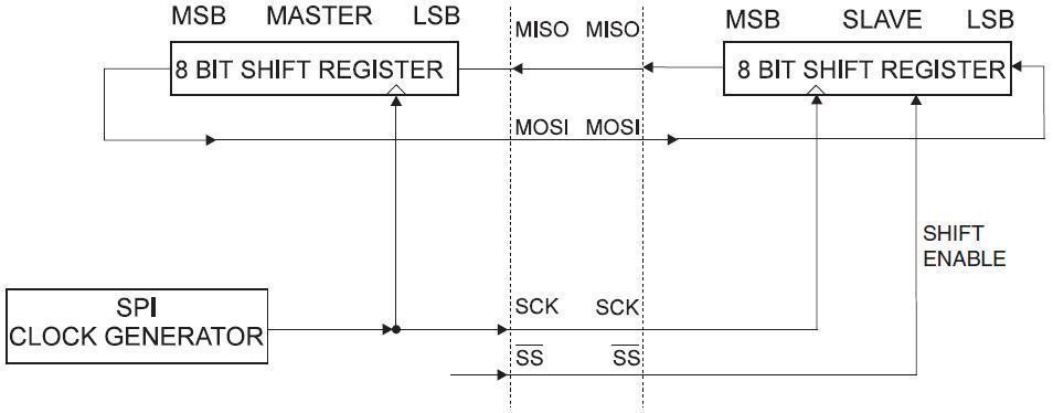
A conceptual representation of how the ATmega SPI subsystem works with our Arduino Proto-shield is shown in Figure 7 “SPI Master-slave Interconnection.” You can find the original of this picture in Section 18 “SPI – Serial Peripheral Interface” in the ATMEL doc8161.pdf document. On the left is the SPI subsystem, it includes the 8-bit Shift Register and the SPI Clock Generator. To send 8 bits of data to the Arduino proto-shield you simply need to write to this register. The SPI subsystem takes care of the reset including generating the serial data stream and clock signal. On the right is an 8-bit shift register used to convert the serial data stream back to 8 discrete bits of data. For our proto-shield this 8-bit shift register is physically realized as a single 74HC595 Serial-to-Parallel shift register. Two generate the 16 output bits used on the proto-shield we daisy chain two 74HC595s and write to the SPI’s 8-bit shift register twice.
The SPI_Shield.inc Include File
To simplify your life – it is after all the first lab – I have already written all the assembly code you need to work with the Proto-shield. This code is contained in a separate file named spi_shield.inc. We will add this file to our program in the same way we included the m328pdef.inc “include” document an earlier part of this lab. Let’s begin.
- Download and add to your Lab1 project folder my spi_shield.inc file.
- Unlike, the m328pdef.inc file which contains equate statements, the spi_shield.inc file includes subroutines which need to be run by the microcontroller.
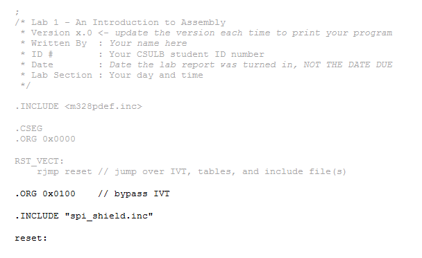
- Add the following lines of code to your Lab1 project file. Original code that you should have already added is shown in gray.
 Quick Review and New Instructions for the Assembler
- Can you Identify the comments?
- Can you tell which lines contain Assembly Directives and which contain Assembly Instructions? Remember assembly directives typically, but not always start with a period and use upper case letters; while assembly instructions use lower case letters.
Do you remember the first INCLUDE assembly directive from earlier in the lab? The m328pdef.inc library is written by Atmel and allows you to use names in place of numbers. For example PINC which was introduced in lab 1 is equated to the number 0x06 in the library. Here is the actual equate statement from the library.
.EQU PINC = 0x06
So when you press the reset button, the AVR processor will first run the rjmp reset instruction. The rjmp instruction tells the processor to jump to the code starting at the reset label. This means the program will jump over (bypass) a table known as the IVT (to be covered later in the semester) and all the code included in spi_shield.inc. Which is a good thing; because we do not want to run any of the included programs until we are ready.
I wrote the spi_shield library. This library includes subroutines InitShield, ReadSwitches, WriteDisplay which allow you to work with the Arduino Proto-shield without knowing the details of how it works.
Why are the two include files placed at different locations in the program?
The m328pdef.inc library is written by Atmel and allows us to use mnemonics (abbreviations like PINC) in place of numbers (like hexadecimal 6). To allow us to use these mnemonic names as quickly as possible we insert this library at the beginning of the program. The spi_shield library is written by the instructor and contains instructions. This code must not be executed at reset so the library is inserted after the first jump instruction (rjmp reset) and above the label reset.
If you have played around with the Arduino IDE, you know that all Arduino programs have an initialization section named setup() and a looping section named loop(). Our assembly program written within the AVR Studio IDE will be configured in a similar fashion. In our case, the initialization section is labeled reset: and the looping section is again named loop:. In the next section you will write the initialization section to be used throughout the semester.
Initialization Section
How to Initialize the Stack
To accomplish almost anything useful in assembly you write a subroutine. To allow us to work with the Proto-shield I have written a number of ready-made subroutines for you to use. When you call a subroutine you need to save your current location on a stack. All computers have built-in hardware stack support. However, before we can save our return address on the stack we need to initialize our stack pointer (SP) register. You will learn more about stacks as the semester progresses. Add the following lines of code to your program right after the reset label.
ldi    r16,high(RAMEND)    // SP = 0x08FF
out    SPH,r16
ldi    r16,low(RAMEND)
out    SPL,r16
How to Use the InitShield Subroutine
We are now ready to call our first subroutine. Add the following line to your program.
call InitShield
The InitShield subroutine takes care of all the initialization required to use the Arduino Proto-shield. You only need to call it once at the beginning of your program, just after stack initialization. That is it, you are now ready to use the ATmega328 GPIO Ports and SPI subsystem to work the Arduino Proto-shield – allowing you to read the 8 switches and whenever you want to update the 7 segment display and/or 8 discrete LEDs. To make your life even simpler the spi_shield file also includes the subroutines ReadSwitches and WriteDisplay.
Looping Section
To programmatically connect our switches to the 7 Segment display we will (1) read the 8 switches into register r6, (2) move register r6 into r7, and (3) then write r7 to the 7 Segment display. We will maintain the connection by looping the program around these three instructions using the Relative Jump (rjmp) instruction. To accomplish steps 1 and 3 you will use two subroutines that I have already written for you named ReadSwitches and WriteDisplay. In the next two sections we will take a closer look at both.
You can find out more about these and other instructions in AVR Studio by clicking Help in the menu bar and selecting Assembler Help. Let’s take a little closer look at our program and how it works.
How to Use the ReadSwitches Subroutine
In Figure 6, on the left hand side, you see bits in Register 6 (in purple) assigned to each of the 8 switches. Register 6 is not hardwired to the switches. Instead, we will use the ReadSwitches subroutine to read the GPIO ports and perform all the logical operations needed to map these switches to Register 6.
Remember, changing the switches does not automatically change the value in register r6 – you must call ReadSwitches.
How to Use the WriteDisplay Subroutine
In Figure 6, on the right hand side, you see bits in Register 7 and Register 8 (in purple) assigned to each of the lines controlling the input pins of the 7 segment display and 8 discrete LEDs. To change the 7 segment display or any one of the discrete LEDs, you make the change to bit(s) within the associated register and call the WriteDisplay subroutine. The WriteDisplay subroutine will take care of all of the housekeeping required to map these bits within the registers to their corresponding pins. Please, do not get confused. These registers are not hardwired to the 7 segment display and discrete LEDs. Instead they are used as arguments to the WriteDisplay subroutine which sends them to the SPI Serial Register, which in turn sends them as a serial stream of data to the 74HC595 ICs on the Arduino Proto-shield (see Figure 7).
If you are asking yourself “What is a 7 segment display?” and “What is a 74HC595?” among probably many other questions, you can find many of your questions answered in Appendix B “How the Parts of the Arduino Proto-Shield Work.”
Remember, changing bits within these registers does not automatically change the pins on the 7 segment display or discrete LEDs – you must call WriteDisplay.
In the next section we will see how the ReadSwitches and WriteDisplay subroutines can be used to create software wires between the 8 switches and 7 Segment display.
Making SPI Software Wires
Because the switches are not physically connected to the 7 segment display, we must create software wires to transfer the data. In this section, we want to connect all 8 switches to their corresponding segments of the 7 Segment display (the numeric display on the top right in Figure 8) using our two new subroutines and a new assembly instruction. Once you have completed this section, the CSULB shield should work as discussed in the questions from Prelab 1.
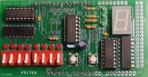
Let’s review what you have accomplished to date. In “The SPI_Shield.inc Include File” section you initialized the stack pointer and included SPI subroutines InitShield, ReadSwitches, and WriteDisplay. You ended by calling InitShield to setup the SPI Subsystem of the ATmega328P microcontroller.
In the “How to Use the ReadSwitches Subroutine” section you learned how to connect the 8 switches on the Proto-board to Register 6 (in purple) as illustrated on the left hand side of Figure 8. In the “How to Use the WriteDisplay Subroutine” section you learned how Register 7 and Register 8 (in purple) can control the input pins of the 7 segment display and 8 discrete LEDs. To make our software wires we simply need to move the contents of Register 6 into Register 7. To do that, we will use the assembly mov instruction. Add the following lines to your program.
The rjmp instruction loops back so that future changes made to the switches are sent to the 7 segment display.
On Your Own
Apply what you have learned by connecting the 8 switches to the eight discrete LEDs. Add the appropriate instruction to do this to the main loop. Like the 7 segment display which is mapped to register r7, the eight discrete LEDs are mapped to register r8. Your code should now update both the 8 discrete LEDs and 7 segment display. You only need to call the WriteDisplay subroutine once.
Debug Workshop 1 — Simulate Your Program
Important The following section summarizes what you learned in Debug Workshop 1 covered in Lab 1 Part A and introduces the step over button ![]() to skip over subroutine calls. You must complete this section before starting lab 2. You may/will be tested (ex. Quiz 1) on the information contained in both Debug Workshops (1 and 2) plus you will need to demonstrate proficiency with the simulator (i.e., debugger) as part of the sign-off for lab 1.
to skip over subroutine calls. You must complete this section before starting lab 2. You may/will be tested (ex. Quiz 1) on the information contained in both Debug Workshops (1 and 2) plus you will need to demonstrate proficiency with the simulator (i.e., debugger) as part of the sign-off for lab 1.
PLEASE REFER TO THE SIMULATION TUTORIAL FOR ADDITIONAL INFORMATION AND TO UNDERSTAND WHAT YOU ARE DOING.
Assemble your program by pressing the Assemble F7 ![]() icon. If there are no syntax errors you should see the following line in the Build window pane (usually located at the bottom of the screen).
icon. If there are no syntax errors you should see the following line in the Build window pane (usually located at the bottom of the screen).
Assembly complete, 0 errors. 0 warnings
Important – Reading and Remembering can SAVE HOURS OF TIME!
- One very common misconception is that when the assembler says there are 0 errors and 0 warnings that your program will work. That is almost always not the case! This message only tells you that the assembler understood everything you entered. Technically speaking, it is saying that your syntax is correct. Unfortunately, ninety-nine times out of a hundred your program still contains “programming” or logical errors. You have to find these errors all by yourself. Luckily, AVR Studio includes a Simulator to help you.
- Students try to make their broken programs work by making random changes and downloading them to their Arduino boards to see if they “now” work. This process is repeated for hours upon hours until more errors are introduced than corrected. I typically receive an email after 4 to 8 hours of frustration, asking why the program doesn’t work. The first thing I ask is if they have simulated the program. The typical answer is NO. One of the reasons I am including this lab at this early stage in the course, is so you cannot download to your Arduino board and so make this common mistake. ALWAYS SIMULATE YOUR PROGRAM.
Once your program has assembled successfully enter AVR Studio’s debug mode by pressing the Assemble and Run ![]() icon.
icon.
If closed, expand the Registers folder in the Processor pane and PORTC and PORTD in the I/O View pane within AVR Studio. Select PORTD. In the window below the I/O View, you will notice that PORTD has three rows of eight bits, represented by square boxes.
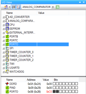
Each box corresponds to a flip-flop or pin as defined in Table 1 “Port Pin Configurations.”
| Inputs | Outputs | |||
|---|---|---|---|---|
| DDRXn | PORTXn | I/O | Pull-up | Comments |
| 0 | 0 | Input | No | Read “Synchronized” PINXn |
| 0 | 1 | Input | Yes | |
| 1 | X | Output | N/A | Write bit to PORTXn |
[/av_textblock]
[av_textblock size=” font_color=” color=” av-medium-font-size=” av-small-font-size=” av-mini-font-size=” admin_preview_bg=”]
Looking at Figure 9, lets start with the first row and the Port D Data Direction Register (DDRD). Each box in this row corresponds to flip-flop. As defined in Table 1, if this box is filled in (Flip-Flop DDRXn = 1) then this port pin will be an output. Conversely, if the box is not selected then the port pin will be an input.
The second row of Figure 9 may be visualized as a physical Port D pin (PIND). If you want to simulate a change on an input pin, say from a switch being toggled, this is the box you would set (input = 1) or clear (input = 0).
The third row contains the Port D register (PORTD). Each box in this row corresponds to flip-flop PORTxn. As described in Table 1, these flip-flops are interpreted differently based on if the port pin is defined as an input (DDRXn = 0) or an output (DDRXn = 1). If DDRXn = 0 (input), then the corresponding PORTXn flip-flop adds (PORTXn = 1) or removes (PORTXn = 0) a Pull-up resistor (see fourth column in Table 1). If DDRXn = 1 (output), then the corresponding PORTXn flip-flop defines the output state of the pin. For example, if PORTXn = 1, the pin is driven high. If you want to see how your program modifies a pin defined as an output, PORTXn is the box you would look at.
As an example, lets assume all Port D pins are to be inputs with pull-up resistors assigned to the two most significant inputs. In this case all the boxes in the DDRD (second row) would be empty (logic 0) and the two most significant boxes of the last row would be filled in (logic 1). This is the case depicted in Figure 9.
The above example corresponds to switches 7 and 6. To simulate turning a switch ON simply check the box corresponding to the desired input pin (PIND).
By clicking on the Step Over (F10) ![]() button, single step the program to the last line of your program.
button, single step the program to the last line of your program.
Now, open the PORTC window by selecting PORTC in the I/O View window.
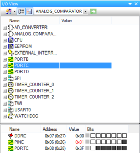
Let’s simulate switch SW0 in the up/ON position (logic 1) by checking the first box in the PINC Register.
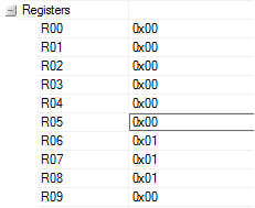
With respect to Table 1 “Port Pin Configurations” and the above image (Figure 10), note that PORT C bit 0 has been configured as an input with a pull-up resistor and the input is currently at logic 1. If it is not already open, expand the Register entry in the Processor window pane (normally located in the upper-left window pane). Notice that register R06 is cleared (0x00)
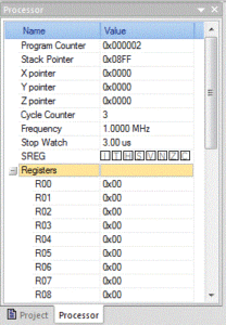
Single step (using Step Over) through your program so the input instruction is executed:
call ReadSwitches // read switches into r6
In the Processor window you should now see r06 now set to 1 (0x01).
Single step your program so the output instruction is executed:
call WriteDisplay // write r7 to the 7 segment display
If you have followed the lab instructions exactly and correctly written your one line of code, you should now see the following in the processor window:
Lab Sign-off
At signoff, you will be given an arbitrary hexadecimal number. You should be able to convert this number to binary and simulate the corresponding switch configuration using the PINC and PIND registers in AVR Studio. You should also be able to use the processor window to demonstrate that your program does, in fact, programmatically “wire” the switches to the 7-segment display (r7) and discrete LEDs (r8).
For example: given 0xA2, input 0b10100010 into PINC and PIND registers.

How to Create and Print-out a List (.lst) File
At the end of each lab, you will turn in a List file version of your program. A list file contains both your assembly program and the machine program generated by the assembler. First let’s verify that AVR Studio is set to generate a List file. In the menu bar select Project and then Assembler Options
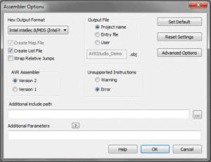
Now whenever you assemble your program, a file with a .lst extension will be created in your project folder. Assemble your program and then open the generated list file.
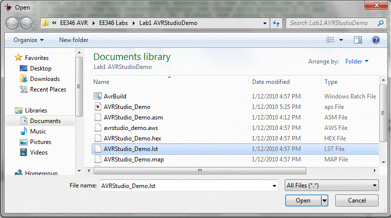
You will see that along with your program the list file includes a lot of other stuff. Most of this is the text from the included m328pdef.inc document. This is the document that includes all the equate Assemble Directives which allow us to use mnemonics for all our registers in place of their actual addresses. If you have not done so already browse this material to see how AVR Studio does it. You should see something like the following.
AVRASM ver. 2.2.7 c:\users\Documents\Lab1\Lab1.asm Tue Aug 21 13:05:53 2018

[builtin](2): Including file 'C:/Program Files (x86)\Atmel\Studio\7.0\Packs\atmel\ATmega_DFP\1.2.209\avrasm\inc\m328pdef.inc'
c:\users\Documents\Lab1\Lab1.asm(10): Including file 'C:/Program Files (x86)\Atmel\Studio\7.0\Packs\atmel\ATmega_DFP\1.2.209\avrasm\inc\m328pdef.inc'
c:\users\Documents\Lab1\Lab1.asm(16): Including file 'c:\users\Documents\Lab1\spi_shield.inc'

/* Lab 1 - An Introduction to Assembly

* Version x.0 <- update the version each time to print your program
* Written By : Your name here
* ID # : Your CSULB student ID number
* Date : Date the lab report was turned in, NOT THE DATE DUE
* Lab Section : Your day and time
*/

;***** Created: 2011-02-09 12:03 ******* Source: ATmega328P.xml **********
;*************************************************************************
;* A P P L I C A T I O N N O T E F O R T H E A V R F A M I L Y
;*
;* Number : AVR000
;* File Name : "m328Pdef.inc"
;* Title : Register/Bit Definitions for the ATmega328P
;* Date : 2011-02-09
There is a lot of extra material that is not useful, so there are several things to remove. Everything that comes from any include file must be removed since it is not a part of the main code. Delete material from this line…
;***** Created: 2009-12-11 15:36 ******* Source: ATmega328P.xml **********
;*************************************************************************

up to and including this line.

; ***** END OF FILE ******************************************************
Your list file must include the AVR Studio Assembler version and time stamp!
AVRASM ver. 2.1.42 Tue Aug 23 16:57:15 2011
The “Resource Use Information” should also be deleted before you print out your list file.
Delete material from this line…
RESOURCE USE INFORMATION
------------------------
up to, but not including this line.
Assembly complete, 0 errors, 0 warnings
You can clean up and format the final version of your file in AVR Studio or your favorite text editor. Regardless of the text editor your final document should be formatted as follows.
Font: Courier or Courier New
Size: 9 or 10 point
Paragraph Spacing: 0 pt before and after
Line Spacing: Single
Page Layout: Landscape
Next, clean up unwanted spaces so your code is aligned and easy to read. DO NOT FORGET THIS STEP. Your touched up list file should now look something like this template.
AVRASM ver. 2.1.42 Tue Jan 10 11:24:47 2013 /* Lab 1 - An Introduction to Assembly * Version x.0 <- update the version each time to print your program * Written By : Your name here * ID # : Your CSULB student ID number * Date : Date the lab report was turned in, NOT THE DATE DUE * Lab Section : Your day and time */ .CSEG .INCLUDE.ORG 0x0000 RST_VECT: 000000 c131 rjmp reset // jump over IVT, tables, and include files .ORG 0x0100 // place all the code that follows starting at the address 0x0100. .INCLUDE "spi_shield.inc" reset: // Initialize the stack pointer 000132 e008 ldi r16, HIGH(RAMEND) // IO[0x3e] = 0x08 000133 bf0e out SPH, r16 000134 ef0f ldi r16, LOW(RAMEND) // IO[0x3d] = 0xFF 000135 bf0d out SPL, r16 000136 940e 0100 call InitShield loop: 000138 940e 0116 call ReadSwitches // read switches into r6 00013a 2c76 mov r7,r6 // wire switches to the 7 segment display 00013b 940e 0121 call WriteDisplay // write r7 to the 7 segment display 00013c cffb rjmp loop Assembly complete, 0 errors, 0 warnings
NOTE: THIS IS JUST AN EXAMPLE. YOUR LIST FILE SHOULD CONTAIN THE CODE FOR THE LAB YOU ARE SUBMITTING.
Finally, if you have not done so already, set your printer page layout to landscape mode. Preview your printout before you actually print it out to save paper. Double check your document to make sure there is no word wrap. Your printout should never include word-wrap. If you do see a line wrapping in the print-out, go back and correct the line and re-print your list file. Print your list file.
Now single step ![]() your program noting how the change input modify the registers. Use the step over button
your program noting how the change input modify the registers. Use the step over button ![]() to skip over the subroutine call instructions. This button tells the simulator to run the code in the subroutine without showing you.
to skip over the subroutine call instructions. This button tells the simulator to run the code in the subroutine without showing you.
Follow the instructions in Lab 1 “Debug Workshop 1” to simulate your program and verify your program reads the switches and moves them to register r7. Until you actually build your own proto-shield you will have to assume that my WriteDisplay subroutine works.
Design Challenge (2 Points)
You can skip this section if you are happy receiving a passing or even a good grade on the lab. If you want to receive an excellent grade you will need to accept the challenge. Specifically, the maximum grade you can receive on this lab if you do not accept the challenge is 18 points.
The purpose of this design challenge is to help you better understand how the I/O ports work and to how the subroutines ReadSwitches and WriteDisplay are written.
The SPI Shield which you will be assembling soon has two green status LEDs. They are connected to the two least significant bits of PORTB, as shown in Figure 15. The design challenge for Lab 1 is to create software “wires” between switches 6 and 3, connected to PIND6 and PINC3, and these two green LEDs. Make sure that switch 6 connects to PORTB1 and switch 3 goes to PORTB0.
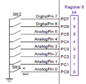
This can be accomplished by implementing something similar to the ReadSwitches subroutine, where the inputs are read from the desired I/O port and then written to the output I/O port. Refer to Appendix A for an explanation of how the InitShield and ReadSwitches subroutines work. Note that if you are correctly calling the InitShield subroutine, you do not need to modify any of the Data Direction Registers (DDRx). PORTB should look like this if both LEDs are turned on after correct execution of this challenge:

Lab 1 Deliverable(s) / Checklist
STOP Read the Lab READ ME document contained in the Labs Folder. Be absolutely sure you have followed all instruction in the “Lab Formatting” section of this document. Points will be deducted if you do not follow these instructions. You have been warned.
If you have not done so already, please purchase a Lab Notebook. Follow the guidelines provided in the “Lab Notebook” section of the Lab READ ME document.
Make sure you have read and understand the “Plagiarism” section of the Lab READ ME document, especially if you are repeating the class.
All labs should represent your own work – DO NOT COPY.
Remember before you turn in your lab…
- Does your software program “wire” the switches to the 8 discrete LEDs and the 7 segment display?
- Your lab report includes a title page with your picture (one that will allow me to match a name with a face), lab number, your name, today’s date, and the day your lab meets
- The above information is duplicated in the title block of your assembly program as described in the lab. Do not forget to include the first line of your program containing the title of the lab. If you are not careful this line may be deleted and points deducted.
- Your list file should include the AVR Studio Assembler version and time stamp.
- Your list file should not include material from the m328pdef.inc or spi_shield libraries or Resource Use Information.
- Include the Assembly line indicating that your Assembly program contains no errors or warning in syntax.
- Your list file should be formatted as defined here.
Font: Courier or Courier New
Size: 9 to 10.5 point
Paragraph Spacing: 0 pt before and after
Line Spacing: Single - All fields within the program area (address, machine instruction, label, operand, destination operand, source operand, comment) must be aligned.
- Your list file printout should be in landscape and not have any lines wrap from one line to the next.
- Never turn in a program that is not debugged (i.e., contains logical errors).
[/av_textblock]
[av_textblock size=” font_color=” color=” av-medium-font-size=” av-small-font-size=” av-mini-font-size=” admin_preview_bg=”]
[expand title=”Appendix” tag=”h3″]
Appendix A: A Quick Look at SPI_Shield
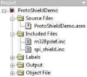
To look at the assembly code in spi_shield.inc; inside the Project window, double-click the spi.inc file in the Included Files folder. You may need to reassemble ![]() the program if the folder is empty.
the program if the folder is empty.
You should now be able to tab between the Lab2.asm (named ProtoShieldDemo in the screen capture) and spi_shield.inc files open in the Workspace window. In the Workspace window select the Lab2.asm tab to view this file.
How the InitShield Subroutine Initializes the GPIO Ports C and D
We begin by initializing PORT D bits 7 to 6 and PORT C bits 5 to 0 as inputs with pull-up resistors. To find out the correct bit settings study Table 1 “Port Pin Configurations.”
| DDRXn | PORTXn | I/O | Pull-up | Comments |
| 0 | 0 | Input | No | Read “Synchronized” PINXn |
| 0 | 1 | Input | Yes | |
| 1 | X | Output | N/A | Write bit to PORTXn |
In this lab we want to configure 8 switches so a byte wide solution makes the most since. The Set Bit(s) in Register (sbr) and Clear Bit(s) in Register (cbr) assembly instructions provide us with our 8-bit solution. The sbr and cbr work with registers, so we will have to first load the Data Direction registers (DDRC, DDRD) and PORT (PORTC, PORTD) registers into one of our 32 general purpose registers, before you can set or clear any of the bits. The sbr, cbr give us the ability to set or clear multiple bits. This is done by setting the bit you want set or cleared to 1, with 0 indicating don’t change.
Reviewing Figure 1 you will notice switches 7 and 6 are wired to Port D bits 7 and 6 and switches 5 to 0 are wired to Port C bits 5 to 0. Consequently, it is these bits within the two Ports that we want to configure as required by Table 1 “Port Pin Configurations.” Study the comments following each of the instructions below to see how this was done.
; Initialize Switches with Pull-up resistors and Test LEDs
in r16,DDRC // input Port C DDR (0x07) for switches 5 to 0
cbr r16,0b00111111 // define bits 5 to 0 as input (clear bit reg.)
out DDRC,r16 // output
in r16,PORTC // input Port C Reg. (0x08) for switches 5 to 0
sbr r16,0b00111111 // add pull-up resistors (PUR)
out PORTC,r16 // output
in r16,DDRD // input Port D DDR (0x0A) for switches 7 to 6
cbr r16,0b11000000 // define bits 7 to 6 as input (clear)
out DDRD,r16 // output
in r16,PORTD // input Port D Reg. (0x0B) for switches 7 to 6
sbr r16,0b11000000 // add pull-up resistors (PUR)
out PORTD,r16 // output
How ReadSwitches Subroutine Maps the 8 Switches to General Purpose Register 6
In this section I am going to show you how I wrote the code to wire the 8 switches to their corresponding bits in Register 6. This virtual connection of the switches to Register 6 is illustrated on the left hand side (in purple) in Figure 1.
Looking at Figure 1 you will notice that while switches 7 and 6 are wired to Port D bits 7 and 6, switches 5 to 0 are wired to Port C bits 5 to 0. Consequently, I needed to read the pins of both ports and then concatenate bits 7 and 6 of Port D with bits 5 to 0 of Port C.
loop:
; SPI Software Wires
in r17, PINC // input port C pins (0x06) into register r17
in r16, PIND // input port D pins (0x09) into register r16
Before I could concatenate (combine) the two registers I needed to clear the unused bits. The Clear Bit(s) in Register (cbr) assembly instructions works perfectly when you want to selectively clear more than one bit while not modifying other bits within the destination register.
cbr r17, 0b11000000 // clear non-switch bits 7 and 6
cbr r16, 0b00111111 // clear non-switch bits 5 to 0
The notation 0b tells the assembler that the following bits are in binary. So 0b11000000 = 110000002. I could just as easily have typed 0xC0. In this case I used binary to more easily show which bits were being cleared (a 1 is placed in the position to be cleared) and which were not being modified (a 0 is placed in the position to not be modified). Finally, I was ready to combine the bits. The logical or operator is used to accomplish this goal. Reviewing what you learned in your Digital Logic Design class.
| x | y | x OR y | |
| 0 | 0 | 0 | |
| 0 | 1 | 1 | |
| 1 | 0 | 1 | |
| 1 | 1 | 1 |
Because I had set to 0 the bits to be set or cleared by the other register, we only need to look at the first two lines in the table to see how it works. If the target bit is 0 it will remain 0 and if it is 1 it will remain 1. After we have merged our two registers we move the result into register 6 as required by Figure 1.
or r16, r17 // concatenate switches SW7 – SW6 : SW5 – SW0
mov r6, r16 // move to standardized switch register
; SPI interface registers
.DEF spiLEDS=r8
.DEF spi7SEG=r7

; Switches
.DEF switch=r6

; Temporary storage of AVR Status REGister Flag bits
.DEF reg_F=r15

; 7-segment display
.EQU seg_a=0
.EQU seg_b=1
.EQU seg_c=2
.EQU seg_d=3
.EQU seq_e=4
.EQU seg_f=5
.EQU seg_g=6
.EQU seg_dp=7

InitShield:
; Disable interrupts and configure stack pointer for 328P
cli

; Initialize Switches with Pull-up resistors and Test LEDs
in r16,DDRC        // input Port C Data Direction Register (0x07) for switches 5 to 0
cbr r16,0b00111111 // define bits 5 to 0 as input (clear bit register)
out DDRC,r16       // output

in r16,PORTC       // input Port C Register (0x08) for switches 5 to 0
sbr r16,0b00111111 // add pull-up resistors (PUR)
out PORTC,r16      // output

in r16,DDRD        // input Port D Data Direction Register (0x0A) for switches 7 to 6
cbr r16,0b11000000 // define bits 7 to 6 as input (clear)
out DDRD,r16       // output

in r16,PORTD       // input Port D Register (0x0B) for switches 7 to 6
sbr r16,0b11000000 // add pull-up resistors (PUR)
out PORTD,r16      // output

; Initialize SPI Port
in r16,DDRB        // Input from Port B Data Direction Register (DDRB) at i/o address 0x04
sbr r16,0b00101111 // Set PB5, PB3, PB2 (SCK, MOSI, SS) and PB1, PB0 (TEST LEDs) as outputs
out DDRB,r16       // Output to Port B Data Direction Register (DDRB) at i/o address 0x04

ldi r16,0b01010001 // Set SPCR Enable (SPE) bit 6, Master (MSTR) bit 4, clock rate fck/16 (SPR1 = 0,SPR0 = 1)
out SPCR,r16       // Output to SPI Control Register (SPCR) at i/o address 0x2c

cbi PORTB,2 // Clear I/O Port B bit 2 (SS) at i/o address 0x05
cbi PORTB,1 // Clear I/O Port B bit 1 (TEST LED1)
cbi PORTB,0 // Clear I/O Port B bit 0 (TEST LED0)
ret

ReadSwitches:
; SPI Software Wires
push r17
push r16

in r17, PINC // input port C pins (0x06) into register r17
in r16, PIND // input port D pins (0x09) into register r16

cbr r17, 0b11000000 // clear non-switch bits 7 and 6
cbr r16, 0b00111111 // clear non-switch bits 5 to 0

or r16, r17 // concatenate switches SW7 - SW6 : SW5 - SW0
mov r6, r16 // move to standardized switch register

pop r16
pop r17
ret

WriteDisplay:
; Save SREG
push reg_F
in reg_F, SREG
; Start transmission of data
out SPDR,spiLEDS
rcall spiTxWait
out SPDR,spi7SEG
rcall spiTxWait
sbi PORTB,PB2 // strobe latches
cbi PORTB,PB2
; Restore SREG
out SREG, reg_F
pop reg_F
ret

SpiTxWait:
push r16
; Wait for transmission complete
spiPolling:
in r16,SPSR
bst r16,SPIF
brtc spiPolling
pop r16
ret

; --------------------------
Appendix B: How the Parts of the Arduino Proto-Shield Work
This appendix was written by Bryan Everett, and is designed for the student who does not want to wait to find out how the proto-shield works. In addition to this material you may also want to read “ATmega328P Serial Communications.”
The 74HC595 Shift Register
The 74HC595 is a high speed CMOS shift register. It has one serial data input with eight (8) parallel output. In this section we will learn how each of these pins control the 74HC595 shift register and what is going on inside the “595”
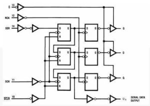
Let’s discuss the components that make up the 74HC595 shift register.
Tri-State Output Buffers
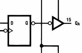
The eight parallel-out pins of this shift register are driven by tri-state buffers. A tri-state buffer is a device commonly used on shift registers, memory, and many other kinds of integrated circuits.

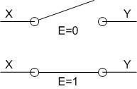
The tri-state buffer shown above has two inputs, data (X) and control (E), which control the state of the output (Y). Just as the name implies, there are three output states: high, low and high impedance. When the pin labeled “E” is high, the output is equal to the input (Y=X).
Not very interesting, right? Well, when the pin labeled “E” is low, the output is in high impedance mode. In high impedance mode, the output is virtually disconnected from the input, neither high nor low. The basic operation of a tri-state buffer can also be easily understood if compared to a switch. When the “E” pin is high, the switch is closed, and when the “E” pin is low, the switch is open. In the context of our shift register, the output pins will either contain our data or will be in high impedance mode.
For more information regarding tri-state buffers, click here.
National Semiconductor – Tri-State Buffer IC
Storage Registers (D Flip-flops)
Looking further into our shift register we see the storage registers. These registers are made up of D-type flip flops. The D-type flip flop is capable of storing one bit of memory. The D-flip flop’s function is to place on the output whatever data is on its input when the flip flop detects a rising edge signal (input buffer inverts clock before input of FF shown) on the clock port. This works by placing the data to be stored (1 or 0) on the D pin. Once the data is on the D line, the clock pin must be pulsed high. On the rising edge of the pulse the data on the D pin will appear on the Q pin.
In context to our shift register, when the data appears on D pins of the storage registers and is ready to be displayed, the clock pin is pulsed and the data is sent to the tri-state buffers.
For more information regarding D-type flip flops, click here.
Fairchild Semiconductors – D-Flip Flop
Shift Registers (D Flip-flops
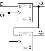
The shift registers are final stage and are made up of D-Flip flops as well. These are the heart of our 74HC595 shift register. Below is a simplified version of what makes our shift registers work. What we have there is two D-type shift registers. The output of the first D flip flop is connected to the input of the second D flip flop. The clock pins are connected together on all D flip flops.
To understand how this shift register works, we will look at a two bit shift register:
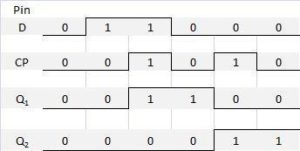
Suppose we want to set Q2 high and Q1 low:
- The D pin is set high.
- The clock pin is pulsed high once. (This makes the output Q1 high. Q1 is connected to the input of the second D flip flop)
- The D pin is brought low.
- The clock is pulsed once again.
- The result is Q1 = 0 and Q2 = 1.
The above example only covers a two bit shift register. Below is the logic diagram of our 74HC595 8-bit shift register.
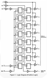
MM74HC595 Logical Diagram by Fairchild Semiconductor
Below is the timing diagram of our 74HC595 8-bit shift register.
MM74HC595 by Fairchild Semiconductors
For more information regarding shift registers, see AllAboutCircuits.com
Seven Segment Display
Just as you learned in EE-201, seven segment displays made up of seven (eight with a decimal point) LEDs arranged and shaped such that numbers between 0 and 9 can be displayed. There are two basic kinds of seven segment displays, common anode and common cathode. This simply means that they share either a supply or ground connection. Other than that, these seven segment displays function just as seven separate LEDs. The Arduino Proto-Shield uses a common cathode display.
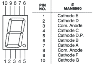
Source: ElectronicsLab – Common Anode.
Each of the segments includes a 1 Kohm resistor to limit current though the LED. The resister values are calculated by: (VDD – VLED)/ILED.
Since the segments function as individual LEDs, see LED Basics for more information.
Appendix C: Reference
- Here is a New York University (NYU) lab for the 74hc595 shift register and the Arduino: http://www.makingthingsmove.org/blog/?p=248
- Serial to Parallel Shifting-Out with a 74HC595, http://www.arduino.cc/en/Tutorial/ShiftOut
- 74HC595 Data Sheet: 8-bit serial-in, serial or parallel-out shift register with output latches; 3-state multiplying arduino outputs/inputs
- Atmel ATmega328 datasheet doc2545.pdf, Section 16 SPI – Serial Peripheral Interface (pages 160 to 162)
- Atmel AVR Microcontroller Primer: Programming and Interfacing by Steven F. Barrett, Section 2.3.3 Serial Peripheral Interface (pages 34 to 39[1]
- Programming and Customizing the AVR Microcontroller by Dhananjay Gadre, Section 6.6.1 I/O Expansion using Shift Register (page 110 to 1111)
- Embedded C Programming and The Atmel AVR 2nd Edition by Richard H. Barnett, Section 2.10 Serial Communication using the SPI (page 151 to 157[2])
- University of Maryland – Tri-state Buffer
- Hobby Projects – D-type Flip Flop
[1] Assumes ATmega16
[2] Assumes ATMega16 and ATMega128
[/expand]
[/av_textblock]
[/av_one_full][av_one_full first min_height=” vertical_alignment=” space=” custom_margin=” margin=’0px’ padding=’0px’ border=” border_color=” radius=’0px’ background_color=” src=” background_position=’top left’ background_repeat=’no-repeat’ animation=” mobile_breaking=” mobile_display=”]
[av_button label=’View Exclusively’ link=’manually,https://www.arxterra.com/ee-346-lab-1/’ link_target=” size=’medium’ position=’left’ icon_select=’yes’ icon=’ue871′ font=’entypo-fontello’ color=’dark’ custom_bg=’#444444′ custom_font=’#ffffff’ admin_preview_bg=”]
[av_hr class=’default’ height=’50’ shadow=’no-shadow’ position=’center’ custom_border=’av-border-thin’ custom_width=’50px’ custom_border_color=” custom_margin_top=’30px’ custom_margin_bottom=’30px’ icon_select=’yes’ custom_icon_color=” icon=’ue808′ av-desktop-hide=” av-medium-hide=” av-small-hide=” av-mini-hide=”]
[/av_one_full]

