By: Alan Valles (Electronics and Control)
Approved by: Ijya Karki (Project Manager)
Table of Contents
Introduction
The purpose of this document is to provide suggestions for the next iteration of the design of the PCB shield for the Biped. These improvements are based on feedback and experience in the manufacturing, design and build of the PCB.
Analysis
The engineering method is an iterative process. There are several suggestions and improvements that can be made to Biped schematics in [2] to improve performance of the system.
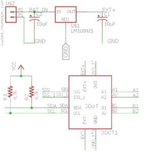
The Schematics since CDR were not revised much. However, after the realized PCB system was put together and tested, there are several updates that I would make for the next revision of the shield. I would add pin headers for the I2C bus. This would allow for flexibility in future iterations for the Biped Project. In the future, I also would have changed the design to incorporate locking headers like the Ph-series of battery and motor connectors for the rest of the external peripherals. These will allow for more secure connections. The combination of jumper wires and pin headers was not a fixed connection and caused major amounts of headache due to contacts not connecting. It lead to perplexing troubleshooting in order to see if bugs were software related or hardware related.
Figure 1. Circuit System.
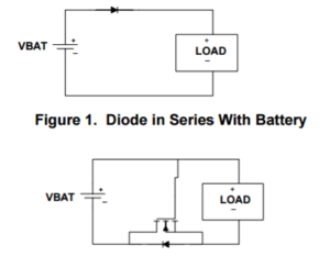
Next, I would add a protection circuit to prevent reverse current in the event of reverse polarity. The chosen lm1084 does not have this built into it. However, the battery was hooked up with reverse polarity the first time. The LM1084 was a robust chip because after reversing polarity of input the LDO still held up fine and output 5V to the rest of the systems. TI offers some quick suggestions to mitigate this issue, by using a protection diode or FET as shown.
Figure 2. NMOS FET in the Ground Return Path.
Next, The Ext- connection was not solidly grounded on the PCB, rather it created a GND connection on the 3Dot board itself. To correct this issue, traces and or vias to GND plane can be created near the connector of the Battery for stronger connection to GND. Finally, another issue was that 3.3V and Ext+ were being paralleled on the PCB that was ordered. After discussion and analysis, the president and I were able to fix this by isolating the connecting point by cutting a copper trace. The GND connection on the shield was never connected to EXT- connection on the 3dot. A small wire was post manufacturing. But the future shield should tie these point together at some point. Also the SDA and SCL lines were crossed for A2D converter so that would obviously be fixed in next iterations.
Figure 3. After PCB in Production.
These are some of the changes that were recognized after our PCB was in production that should be fixed for the next iteration.
Conclusion
In conclusion, the pin headers for encoder connector, and other external peripherals would be changed to a locking style, a reverse current protection circuit would be added and various clean up work would be done such as tying GND to Ext-.
Reference
[1] http://www.ti.com/lit/an/slva139/slva139.pdf
[2] http://arxterra.com/fall-2016-biped-updated-schematics/


