[av_textblock size=” font_color=” color=” av-medium-font-size=” av-small-font-size=” av-mini-font-size=” admin_preview_bg=”]
Serial Communications and I2C
[/av_textblock]
[av_hr class=’default’ height=’50’ shadow=’no-shadow’ position=’center’ custom_border=’av-border-thin’ custom_width=’50px’ custom_border_color=” custom_margin_top=’30px’ custom_margin_bottom=’30px’ icon_select=’yes’ custom_icon_color=” icon=’ue808′ av-desktop-hide=” av-medium-hide=” av-small-hide=” av-mini-hide=”]
[av_textblock size=” font_color=” color=” av-medium-font-size=” av-small-font-size=” av-mini-font-size=” admin_preview_bg=”]
Table of Contents
[/av_textblock]
[av_textblock size=” font_color=” color=” av-medium-font-size=” av-small-font-size=” av-mini-font-size=” admin_preview_bg=”]
Reference(s):
- The AVR Microcontroller and Embedded Systems using Assembly and C by
Muhammad Ali Mazidi, Sarmad Naimi, and Sepehr Naimi, Chapter 18 “I2C Protocol and DS1307 RTC Interfacing” - ATMEL 8-bit AVR Microcontroller with 16/32K Bytes of ISP Flash and USB – ATmega32U4, Chapter 20. 2-wire Serial Interface
- Understanding the I2C Bus, Texas instruments Application Note SLVA704-June 2015
- 7-bit, 8-bit, and 10-bit I2C Slave Addressing by Total Phase
- NXP UM10204 I2C-bus specification and user manual
- Serial Communications (I2C and SPI) Eugene Ho, Stanford University
- Arduino Application Program Examples
- Texas Instruments PCA9535 and PCA9555 16-bit I/O port expanders: Arduino I2C Expansion I/O
- LIS3LV02DQ Accelerometer: Arduino and the Two-Wire Interface (TWI/I2C)
[/av_textblock]
[av_heading tag=’h1′ padding=’10’ heading=’Introduction’ color=” style=” custom_font=” size=” subheading_active=” subheading_size=’15’ custom_class=” admin_preview_bg=” av-desktop-hide=” av-medium-hide=” av-small-hide=” av-mini-hide=” av-medium-font-size-title=” av-small-font-size-title=” av-mini-font-size-title=” av-medium-font-size=” av-small-font-size=” av-mini-font-size=”][/av_heading]
[av_textblock size=” font_color=” color=” av-medium-font-size=” av-small-font-size=” av-mini-font-size=” admin_preview_bg=”]
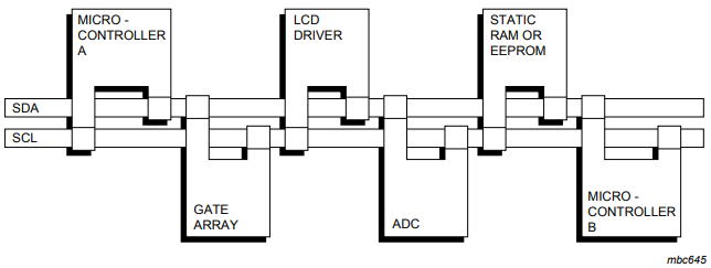
Many embedded systems include peripheral devices connected to the microprocessor in order to expand its capabilities including
- PCA9564 Parallel bus to I2C bus controller
- PCA9685: 16-channel, 12-bit PWM I²C-bus LED controller
- DS1307 RTC (Real-Time Clock), Textbook section 18.4 “DS1307 RTC Interfacing and programming”
- Adafruit Motor Shield SPI
- HM6352 Digital Compass I2C
- BMA180 Triple Axis Accelerometer SPI or I2C
- ITG-3200 Triple–Axis Digital–Output Gyro SPI or I2C
- GPS module USART
- 1.44″ LCD Display USART
Communication methods can be divided into the two categories parallel and serial. All of these peripherals interface with the microcontroller via a serial protocol. A protocol is the language that governs communications between systems or devices. Protocols may specify many aspects of inter-device communications including bit ordering, bit-pattern meanings, electrical connections, and even mechanical considerations in some cases.
The peripheral device may be completely passive; i.e., there is no controlling mechanism in place within the peripheral or complex enough to include an embedded controller, in which case the protocol may be more sophisticated.
There are many questions that need to be answered when defining a serial communications protocol:
- In what order are the series of bits shifted across the data line? Suppose the master transmits the most-significant bit (MSB) first, then the peripheral will receive the series in the order {0, 1, 0, 1, 0, 0, 1, 1}. Alternatively, the master could transmit the least-significant bit (LSB) first; in which case, the peripheral will receive the series {1, 1, 0, 0, 1, 0, 1, 0}. Either method is fine, but the peripheral and master must agree beforehand; otherwise, incorrect bytes will be received.
- What constitutes a CLK event? The master could use either a falling-edge or a rising-edge clock to specify a sampling signal to the peripheral device.
- How does the peripheral know when it is supposed to receive bytes and when it is supposed to transmit bytes?
All of these questions and many more are answered by the protocol. We have already answered these questions for the SPI interface protocol, now it is time to look at the answers for the I2C interface protocol.
[/av_textblock]
[av_heading tag=’h1′ padding=’10’ heading=’Inter-Integrated Circuit (I2C, IIC, TWI) ‘ color=” style=” custom_font=” size=” subheading_active=” subheading_size=’15’ custom_class=” admin_preview_bg=” av-desktop-hide=” av-medium-hide=” av-small-hide=” av-mini-hide=” av-medium-font-size-title=” av-small-font-size-title=” av-mini-font-size-title=” av-medium-font-size=” av-small-font-size=” av-mini-font-size=”][/av_heading]
[av_textblock size=” font_color=” color=” av-medium-font-size=” av-small-font-size=” av-mini-font-size=” admin_preview_bg=”]
Physical Interface
The Inter-Integrated Circuit (I2C or IIC) serial protocol was created by NXP Semiconductors, originally a Philips semiconductor division, to attach peripherals to an embedded microprocessor as shown here. I2C is a multi-point protocol in which peripheral devices are able to communicate along the serial interface which is composed of a bidirectional serial data line (SDA) and a bidirectional serial clock (SCL).
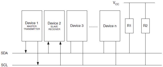
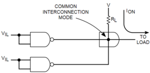
Electrical Interconnection beyond the wires is a single resistor for each of the I2C bus lines. The size of the pull-up resistor is determined by the amount of capacitance on the I2C lines (for further details, refer to I2C Pull-up Resistor Calculation (SLVA689). We will assume a pull-up resistor value of 4.7 kilohm.
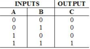
The pull-up resistors along with an open-drain bus structure implement a wired-AND.
Source: Wikipedia, Wired logic connection
In a Wire-AND bus structure, to write a ‘0’ the Master or Slave device pull the line low; otherwise the device leaves the line alone to write a ‘1’, which occurs due to the lines being pulled high externally by the pull-up resistor.
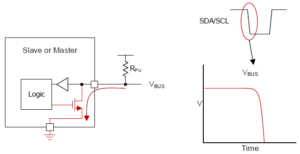

Source: Understanding the I2C Bus, Texas instruments Application Note SLVA704-June 2015
Transferring Bits on the I2C bus is accompanied by a pulse on the clock (SCL) line. The level of the data line must be stable when the clock line is high. The only exception to this rule is for generating start and stop conditions.
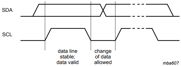
START and STOP conditions are signaled by changing the level of the SDA line when the SCL line is high.

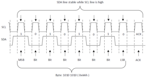
Transferring Packets. All packets transmitted on the I2C bus are 9 bits long. A packet may either be a device address, register address, or data written to or read from a slave. Data is transferred Most Significant Bit (MSB) first. Any number of data packets can be transferred from the master to slave between the START and STOP conditions. Data on the SDA line must remain stable during the high phase of the clock period, as changes in the data line when the SCL is high are interpreted as control commands (START or STOP).
[/av_textblock]
[av_heading tag=’h2′ padding=’10’ heading=’How Many Slave Addresses?’ color=” style=” custom_font=” size=” subheading_active=” subheading_size=’15’ custom_class=” admin_preview_bg=” av-desktop-hide=” av-medium-hide=” av-small-hide=” av-mini-hide=” av-medium-font-size-title=” av-small-font-size-title=” av-mini-font-size-title=” av-medium-font-size=” av-small-font-size=” av-mini-font-size=”][/av_heading]
[av_textblock size=” font_color=” color=” av-medium-font-size=” av-small-font-size=” av-mini-font-size=” admin_preview_bg=”]
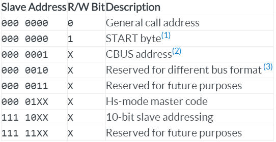
As defined in the NXP I2C-bus specification and user manual or this handy summary article; the I2C uses 7 bits to address peripheral devices. This means a maximum of 27 = 128 devices can be addressed. However, the I2C specification reserves 16 addresses (0x00 to 0x07 and 0x78 to 0x7F) for special purposes as defined in the following table. Therefore for practical purposes the I2C supports up to 128 – 16 = 112 peripheral devices.
[/av_textblock]
[av_heading tag=’h1′ padding=’10’ heading=’Typical Data Transmission’ color=” style=” custom_font=” size=” subheading_active=” subheading_size=’15’ custom_class=” admin_preview_bg=” av-desktop-hide=” av-medium-hide=” av-small-hide=” av-mini-hide=” av-medium-font-size-title=” av-small-font-size-title=” av-mini-font-size-title=” av-medium-font-size=” av-small-font-size=” av-mini-font-size=”][/av_heading]
[av_textblock size=” font_color=” color=” av-medium-font-size=” av-small-font-size=” av-mini-font-size=” admin_preview_bg=”]
The general procedure for a master to access a slave device is the following:
Suppose a master wants to send data to a slave:
- Master sends a START condition and addresses the slave.
- Master sends one or more data packet(s) to the slave.
- Master sends a STOP condition, terminating the transfer.
If a master wants to receive/read data from a slave:
- Master sends a START condition and addresses the slave.
- Master sends the address of the register to read from the slave.
- Master receives one or more data packet(s) from the slave.
- Master sends a STOP condition, terminating the transfer.
An address packet consists of 7 address bits (27 = 128 possible addresses), one READ/WRITE control bit and an acknowledge bit. An address packet consisting of a SLave Address and a READ or a WRITE bit is called SLA+R or SLA+W, respectively. See Figure 10.
A data packet consists of one data byte and an acknowledge bit.

The master begins communication by transmitting a single start bit followed by the unique 7-bit address of the slave device for which the master is attempting to access, followed by read/write bit. The corresponding slave device responds with an acknowledge bit if it is present on the serial bus. The master continues to issue clock events on the SCL line and either receives information from the slave or writes information to the slave depending on the read/write bit at the start of the session. The number of bits transferred during a single session is dependent upon the peripheral device and the agreed-upon higher-level protocol.
As an overview discussion of the I2C bus I am intentionally leaving out a number of interesting subjects including:
- Clock Stretching (See reference textbook “Clock stretching” page 636)
- General call address 0000 000
- Receiver sending a NACK after the final byte. To learn more on NACK read Understanding the I2C Bus, Texas instruments Application Note SLVA704-June 2015.
- Master and slave implementing a hand shake to adjust the clock speed to accommodate the slave.
- Multi-master Bus Systems, Arbitration and Synchronization (Reference textbook “Arbitration” page 636, and “TWI Programming with Checking Status Register” page 668)
[/av_textblock]
[av_heading tag=’h1′ padding=’10’ heading=’Overview of the ATmega328P TWI Module’ color=” style=” custom_font=” size=” subheading_active=” subheading_size=’15’ custom_class=” admin_preview_bg=” av-desktop-hide=” av-medium-hide=” av-small-hide=” av-mini-hide=” av-medium-font-size-title=” av-small-font-size-title=” av-mini-font-size-title=” av-medium-font-size=” av-small-font-size=” av-mini-font-size=”][/av_heading]
[av_textblock size=” font_color=” color=” av-medium-font-size=” av-small-font-size=” av-mini-font-size=” admin_preview_bg=”]
The ATmega328P provides an I2C serial interface via the 2-wire Serial Interface (TWI ) module. The bus allows for up to 128 different slave devices (textbook says 120) and up to 400 kHz data transfer speed. The TWI provides an interrupt-based system in which an interrupt is issued after all bus events such as reception of a byte or transmission of a start condition. The TWI module is comprised of several submodules, as shown here.
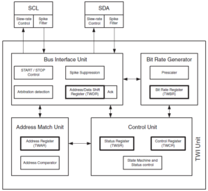
All registers drawn in a thick line are accessible through the AVR data bus.
SCL and SDA Pins contain a slew-rate limiter in order to conform to the TWI specification. The input stages contain a spike suppression unit removing spikes shorter than 50 ns. Enabling the internal pull-ups in the GPIO PORT pins corresponding to SCL and SDA can in some systems eliminate the need for external pull-up resistors (20 – 50 kilohm versus 4.7 kilohm specification).
TWI Bit Rate Register (TWBR)
Bit Rate Generator Unit controls the period of SCL when operating in a Master mode. The SCL period is controlled by settings in the TWI Bit Rate Register (TWBR) and the Prescaler bits in the TWI Status Register (TWSR).


Assuming TWPS1= 0 and TWPS0 = 0 (i.e., 4TWPS = 1) , we have a simple way to calculate TWBR as a function of the SCL frequency.
TWBR = ((CPU Clock frequency / SCL frequency) – 16) / 2
For a desired frequency of SCL frequency = 400 KHz
TWBR = ((8 MHz / 400 KHz) – 16) / 2 = 0x02
The Arduino default SCL frequency is 100 KHz as defined here.
#ifndef TWI_FREQ
#define TWI_FREQ 100000L
#endif
To transmit at 400 KHz you would define TWI_FREQ as 400000L
Note: L is a “literal” meaning Long integer (minimum of 4 bytes = 32 bits).
TWI Data and Address Shift Register (TWDR)
Bus Interface Unit contains the Data and Address Shift Register (TWDR), a START/STOP Controller and Arbitration detection hardware. The TWDR contains the address or data bytes to be transmitted, or the address or data bytes received.

TWI Address Register (TWAR)
Address Match Unit checks if received address bytes match the seven-bit address in the TWI Address Register (TWAR) when the ATmega328P is acting as a slave device. The TWGCE bit enables the recognition of a General Call.

Control Register (TWCR)
Control Unit monitors the TWI bus and generates responses corresponding to settings in the
TWI Control Register (TWCR).

TWINT: TWI INTerrupt Flag
This bit is set by the control unit when requested task is completed and application software response requested.
TWEA: TWI Enable Acknowledge Bit
Generate ACK pulse, if one of three criteria met, .
- Slave address received.
- General call received, while TWAR register’s TWGCE bit is set.
- Data byte received in Master or Slave Receiver mode.
TWSTA: TWI START Condition Bit
Send START condition. Clear when START condition sent (TWINT = 1).
TWSTO: TWI STOP Condition Bit
Send START condition. Automatically cleared when STOP condition sent (TWINT = 1).
TWWC: TWI Write Collision Flag
Indicated write to TWDR when the register is transmitting a byte.
TWEN: TWI ENable Bit
Activate TWI peripheral subsystem. TWI takes control over the I/O pins connected to the SCL and SDA pins.
TWIE: TWI Interrupt Enable
Local TWI interrupt enable bit. If set along with global interrupt bit (SREG I-bit) a TWI interrupt will be requested.
Status Register (TWSR)
When an event requiring the attention of the application occurs on the TWI bus, the TWI Interrupt Flag (TWINT) is asserted. In the next clock cycle, the TWI Status Register (TWSR) is updated with a status code identifying the event.

The TWSR only contains relevant status information when the TWI Interrupt Flag is asserted. At all other times, the TWSR contains a special status code indicating that no relevant status information is available. Status bits TWS7:3 associated with typical I2C serial transmission and reception communication operations without error are defined in the following table and presented in more detail shortly.

[/av_textblock]
[av_heading tag=’h1′ padding=’10’ heading=’Program Examples’ color=” style=” custom_font=” size=” subheading_active=” subheading_size=’15’ custom_class=” admin_preview_bg=” av-desktop-hide=” av-medium-hide=” av-small-hide=” av-mini-hide=” av-medium-font-size-title=” av-small-font-size-title=” av-mini-font-size-title=” av-medium-font-size=” av-small-font-size=” av-mini-font-size=”][/av_heading]
[av_heading tag=’h2′ padding=’10’ heading=’AVR TWI in Master Transmitter Operating Mode’ color=” style=” custom_font=” size=” subheading_active=” subheading_size=’15’ custom_class=” admin_preview_bg=” av-desktop-hide=” av-medium-hide=” av-small-hide=” av-mini-hide=” av-medium-font-size-title=” av-small-font-size-title=” av-mini-font-size-title=” av-medium-font-size=” av-small-font-size=” av-mini-font-size=”][/av_heading]
[av_textblock size=” font_color=” color=” av-medium-font-size=” av-small-font-size=” av-mini-font-size=” admin_preview_bg=”]
In the section entitled “Typical Data Transmission,” I defined three steps for a master to send data to a slave.
- Master sends a START condition and addresses the slave.
- Master sends one or more data packet(s) to the slave.
- Master sends a STOP condition, terminating the transfer.
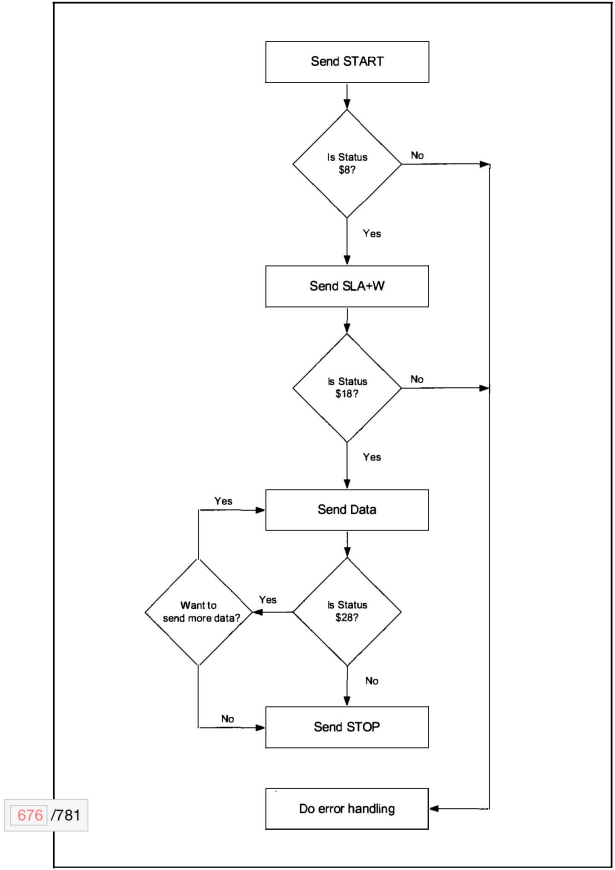
In the next few sections we will look at a master transmitting a single data packet, following these steps, as a ….
- Timeline
- Flowchart
- C++ Code
After the C++ Code example, we will look at how to implement the I2C using the Arduino wire library.
[/av_textblock]
[av_heading tag=’h3′ padding=’10’ heading=’Timeline’ color=” style=” custom_font=” size=” subheading_active=” subheading_size=’15’ custom_class=” admin_preview_bg=” av-desktop-hide=” av-medium-hide=” av-small-hide=” av-mini-hide=” av-medium-font-size-title=” av-small-font-size-title=” av-mini-font-size-title=” av-medium-font-size=” av-small-font-size=” av-mini-font-size=”][/av_heading]
[av_textblock size=” font_color=” color=” av-medium-font-size=” av-small-font-size=” av-mini-font-size=” admin_preview_bg=”]
The following timeline shows the interplay of registers comprising the TWA module. A detailed description of the registers and timeline is outside the scope of this overview article and the interested reader is encouraged to read Section 21.6 “Using the TWI” in the ATmega Datasheet.
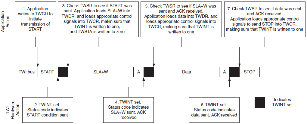
The TWIINTerrupt (TWINT) flag bit is set by hardware when the TWI has finished its current job and expects application software response. The TWINT Flag must be cleared by software by writing a logic one to it.
The application writes the TWI START condition (TWSTA) bit to one when it desires to become a Master on the 2-wire Serial Bus. The TWI hardware checks if the bus is available, and generates a START condition on the bus if it is free. TWSTA must be cleared by software when the START condition has been transmitted.
[/av_textblock]
[av_heading tag=’h3′ padding=’10’ heading=’Flowchart’ color=” style=” custom_font=” size=” subheading_active=” subheading_size=’15’ custom_class=” admin_preview_bg=” av-desktop-hide=” av-medium-hide=” av-small-hide=” av-mini-hide=” av-medium-font-size-title=” av-small-font-size-title=” av-mini-font-size-title=” av-medium-font-size=” av-small-font-size=” av-mini-font-size=”][/av_heading]
[av_textblock size=” font_color=” color=” av-medium-font-size=” av-small-font-size=” av-mini-font-size=” admin_preview_bg=”]
Reference Textbook Section 18.5: TWI Programming with Checking Status Register (page 668) Figure 18-18.
[/av_textblock]
[av_heading tag=’h3′ padding=’10’ heading=’C Code’ color=” style=” custom_font=” size=” subheading_active=” subheading_size=’15’ custom_class=” admin_preview_bg=” av-desktop-hide=” av-medium-hide=” av-small-hide=” av-mini-hide=” av-medium-font-size-title=” av-small-font-size-title=” av-mini-font-size-title=” av-medium-font-size=” av-small-font-size=” av-mini-font-size=”][/av_heading]
[av_textblock size=” font_color=” color=” av-medium-font-size=” av-small-font-size=” av-mini-font-size=” admin_preview_bg=”]
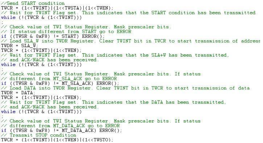
Source: ATmega Datasheet Section 21.6 “Using the TWI”
//                  TWS
#define START       0x01<<3  // 0x08, Start condition transmitted
#define MT_SLA_ACK  0x03<<3  // 0x18, SLA+W transmitted, ACK received
#define MT_DATA_ACK 0x05<<3  // 0x28, Data byte transmitted, ACK received
[av_heading tag=’h2′ padding=’10’ heading=’HMC6352 Digital Compass Arduino Example’ color=” style=” custom_font=” size=” subheading_active=” subheading_size=’15’ custom_class=” admin_preview_bg=” av-desktop-hide=” av-medium-hide=” av-small-hide=” av-mini-hide=” av-medium-font-size-title=” av-small-font-size-title=” av-mini-font-size-title=” av-medium-font-size=” av-small-font-size=” av-mini-font-size=”][/av_heading]
[av_textblock size=” font_color=” color=” av-medium-font-size=” av-small-font-size=” av-mini-font-size=” admin_preview_bg=”]
Source: Compass Heading HMC6352 Sparkfun
I2C HMC6352 compass heading (Sparkfun breakout) by BARRAGAN (http://barraganstudio.com) Demonstrates use of the Wire library reading data from the HMC6352 compass heading.
#include

int compassAddress = 0x42 >> 1; // From datasheet compass address is 0x42
// shift the address 1 bit right, the Wire library only needs the 7
// most significant bits for the address
int reading = 0;

void setup()
{
Wire.begin(); // join i2c bus (address optional for master)
Serial.begin(9600); // start serial communication at 9600bps
pinMode(48, OUTPUT);
digitalWrite(48, HIGH);
}

void loop()
{
// step 1: instruct sensor to read echoes
Wire.beginTransmission(compassAddress); // transmit to device
// the address specified in the datasheet is 66 (0x42)
// but i2c adressing uses the high 7 bits so it's 33
Wire.send('A'); // command sensor to measure angle
Wire.endTransmission(); // stop transmitting

// step 2: wait for readings to happen
delay(10); // datasheet suggests at least 6000 microseconds

// step 3: request reading from sensor
Wire.requestFrom(compassAddress, 2); // request 2 bytes from slave device #33

// step 4: receive reading from sensor
if(2 <= Wire.available()) // if two bytes were received
{
reading = Wire.receive(); // receive high byte (overwrites previous reading)
reading = reading << 8; // shift high byte to be high 8 bits
reading += Wire.receive(); // receive low byte as lower 8 bits
reading /= 10;
Serial.println(reading); // print the reading
}

delay(500); // wait for half a second
}
[/av_textblock]
[av_heading tag=’h2′ padding=’10’ heading=’More Arduino I2C Sketch Examples’ color=” style=” custom_font=” size=” subheading_active=” subheading_size=’15’ custom_class=” admin_preview_bg=” av-desktop-hide=” av-medium-hide=” av-small-hide=” av-mini-hide=” av-medium-font-size-title=” av-small-font-size-title=” av-mini-font-size-title=” av-medium-font-size=” av-small-font-size=” av-mini-font-size=”][/av_heading]
[av_textblock size=” font_color=” color=” av-medium-font-size=” av-small-font-size=” av-mini-font-size=” admin_preview_bg=”]
- Texas Instruments PCA9535 and PCA9555 16-bit I/O port expanders: Arduino I2C Expansion I/O
- LIS3LV02DQ Accelerometer: Arduino and the Two–Wire Interface (TWI/I2C)
- ITG 3200 Triple-Axis Digital-Output Gyro: http://www.arduino.cc/cgi–bin/yabb2/YaBB.pl?num=1278367409/all
[/av_textblock]
[av_heading tag=’h1′ padding=’10’ heading=’Questions’ color=” style=” custom_font=” size=” subheading_active=” subheading_size=’15’ custom_class=” admin_preview_bg=” av-desktop-hide=” av-medium-hide=” av-small-hide=” av-mini-hide=” av-medium-font-size-title=” av-small-font-size-title=” av-mini-font-size-title=” av-medium-font-size=” av-small-font-size=” av-mini-font-size=”][/av_heading]
[av_textblock size=” font_color=” color=” av-medium-font-size=” av-small-font-size=” av-mini-font-size=” admin_preview_bg=”]
- TBD
[/av_textblock]
[av_heading tag=’h1′ padding=’10’ heading=’Answers’ color=” style=” custom_font=” size=” subheading_active=” subheading_size=’15’ custom_class=” admin_preview_bg=” av-desktop-hide=” av-medium-hide=” av-small-hide=” av-mini-hide=” av-medium-font-size-title=” av-small-font-size-title=” av-mini-font-size-title=” av-medium-font-size=” av-small-font-size=” av-mini-font-size=”][/av_heading]
[av_textblock size=” font_color=” color=” av-medium-font-size=” av-small-font-size=” av-mini-font-size=” admin_preview_bg=”]
Using your mouse, highlight below in order to reveal the answers.
- TBD
[/av_textblock]
