By: Victoria Osaji, Manufacturing and Development Engineer
Table of Contents
Introduction:
A printed circuit board (PCB) also known as a printed wiring board is used to build the infrastructure for electronic devices. The purpose of this infrastructure is to mount components and provide the electrical connection between the components in our system, which in our case is the 3DOT board. As part of the subsystem requirements provided: L1-9 Custom PCB-3rd Generation Velociraptor (Th) Project Schedule shall use an external PCB with an I2C Interface (JP5) as the 3DoT Board.
Process:
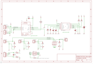
Figure 1: The schematic provided by the E&C that needs to be designed into a PCB.
To design the PCB I used the software Eagle CAD program. I was first given a schematic by our electronics and controls engineer to make into a PCB layout for our project. I imported the schematic and switched it to a board.
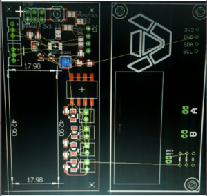
Figure 2: The Screenshot of the connections between the PCB and the 3DOT board after being imported into Eagle CAD
For our project, our PCB had to be designed like a shield for the 3DOT board because of the location we were placing it in. We made the decision to place it right over the square area for the body. As a result of this feature, I needed to make sure that I had made the size and the connections from the 3DOT to the PCB as accurately as possible. Therefore to ensure this accuracy, I imported the 3DOT board from 3DOT library. I then overlapped the 3DOT and the PCB, got the size and connections, and then cut out the power supply part from the PCB because we will not be using it.
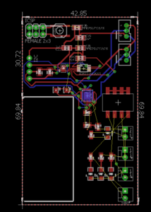
After getting the size and connection where they needed to be, I placed the rest of the other components according to the schematic. I tried to make all the components that were connected to each other close to one another. After the placement of the components or ICs, I began to wire. When wiring I made sure to follow the requirements made by the customer.
Figure 3: Screenshot of what the wiring process looks like.
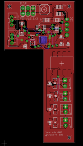
After wiring up everything I ran a couple of design analysis checks to make sure everything required of me and the PCB was met. Then I put some more finishing touches such as copper, the inscription of our project name and class, etc. Since everything was cleared, I got my board approved and then ordered it. Always ensure to order the PCB at least three weeks before the week of the final assembly, especially if ordered by OSH Park, it does take a while to make and get shipped. Also, you would have to solder the board after, so make sure to order the components/parts on the schematic.
Conclusion:
Figure 4: Screenshot of what the final product looks like with the copper and the etching.
All in all, the PCB layout wasn’t hard in its design but time consuming in its conception. Ensuring that I had the right parts in the right location was crucial to the overall success of completion of the PCB. Once it was been determined the reason and overall concept for the PCB design, it was easy and quite fun to do. Thank you and Good luck!
Citation/Guided References:
https://learn.sparkfun.com/tutorials/using-eagle-board-layout
https://www.arxterra.com/printed-circuit-board-pcb-how-to-layout/


