[av_image src=’/wp-content/uploads/2017/05/Fig3Hand-1-255×300.png’ attachment=’25456′ attachment_size=’medium’ align=’center’ styling=” hover=” link=” target=” caption=” font_size=” appearance=” overlay_opacity=’0.4′ overlay_color=’#000000′ overlay_text_color=’#ffffff’ animation=’no-animation’][/av_image]
[av_heading tag=’h3′ padding=’10’ heading=’Spring 2017 Prosthetic Hand: Custom PCB Layout Design’ color=” style=’blockquote classic-quote’ custom_font=” size=’24’ subheading_active=’subheading_below’ subheading_size=’15’ custom_class=”]
The Robot Company | CEO Professor Gary Hill
[/av_heading]
[av_textblock size=” font_color=” color=”]
Blog Post Created by Project Manager | Bianca Esquivel
Project Design Created by Electronics and Controls Engineer | Forest Nutter and Manufacturing and Design Engineer | David Mendoza
[/av_textblock]
[av_heading tag=’h1′ padding=’10’ heading=’Preliminary Information’ color=” style=’blockquote modern-quote’ custom_font=” size=’20’ subheading_active=” subheading_size=’15’ custom_class=”][/av_heading]
[av_icon_box position=’left’ boxed=” icon=’ue864′ font=’entypo-fontello’ title=’Design Objective’ link=” linktarget=” linkelement=” font_color=” custom_title=” custom_content=” color=” custom_bg=” custom_font=” custom_border=”]
In order to control the Hand on this project, it needs two Printed Circuit Boards (PCB) to be wirelessly communicating to each other. One of the PCBs will be placed in the arm and the other in a containment box attached to the customers ankle that would have flex sensors attached on the inside of their shoe.
For the Hand PCB:
Goal:
To create a PCB that is small enough to fit in the Prosthetic Arm storage space. The PCB board should also be able to Connect to Arduino Micro, control the speed and direction of 3 DC motors independently, control a servo, read 3 flex sensors, and hook up to an Xbee to send and receive data.
Working: (referring to the Hand+Arm PCB, but only the hand portion)
The PCB is able to control 3 DC motors independently.
The PCB is able to control 1 Servo.
The PCB is able to read 3 Force sensors.
Problems: (referring to the Hand+Arm PCB, but only the hand portion)
The PCB was not able to send and receive data from the foot pcb.
Since I accidentally returned the xbee shields to hill too early, I was not able to test
(Arduino→ shield → xbee →(wireless) → xbee→ PCB→ Arduino). So I could not determine if the xbee Schematic didn’t work for this PCB.
For the Foot PCB:
Goal:
To create a PCB that is smallest enough to be hidden near the right foot. The PCB board should also be able to connect to Arduino Nano, read 4 Flex Sensors, control 2 vibrating motor’s speed, and hook up to a xbee to send and receive data.
Working:
The PCB is able to read 4 Flex Sensors.
The PCB did output a PWM for the vibrating motors (tested with oscilloscope) but the Voltage was too low likely because of the 3.3v line connected to the 5v line.
Problems:
3.3v label was connected to the Vcc pin of the xbee. I also had another label called Vcc that was connected to my 5v line. I didn’t know that the program would attach labeled wires to pin names. The reason this was fixed on the Hand+Arm schematic was because we changed all the labels so they would not conflict with each other. When the arduino was connected to the PCB it would start to overheat likely because of the 3.3v line being attached to the 5v line. The PCB board was designed to have the Arduino on the top and the xbee on the bottom to save space but neither of them got flipped so, they were both on the top. So even if the PCB did work We could only attach the arduino or the xbee to the board without using wires.
This process is performed in response to requirement:
L1-5 Independence
The prosthetic hand shall be controlled by the customer without the aid of the other hand
[/av_icon_box]
[av_icon_box position=’left’ boxed=” icon=’ue856′ font=’entypo-fontello’ title=’Materials’ link=” linktarget=” linkelement=” font_color=” custom_title=” custom_content=” color=” custom_bg=” custom_font=” custom_border=”]
Eagle CAD Software
[/av_icon_box]
[av_heading tag=’h1′ padding=’10’ heading=’Design Process’ color=” style=’blockquote modern-quote’ custom_font=” size=’20’ subheading_active=” subheading_size=’15’ custom_class=”][/av_heading]
[av_textblock size=” font_color=” color=”]
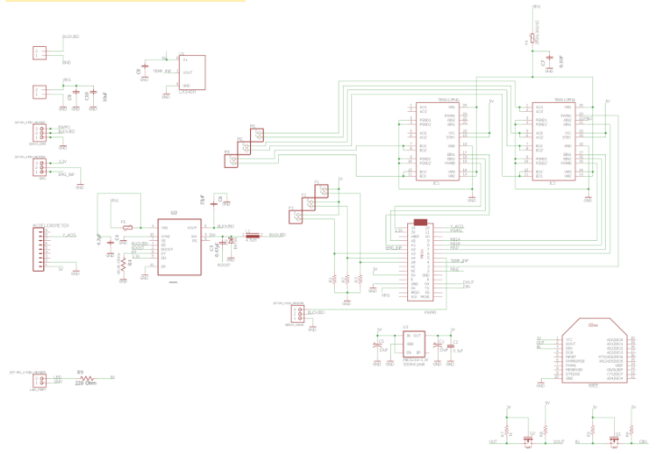
Hand+Arm Schematic by Forest Nutter | Electronics and Control Engineer – Prosthetic Hand and Mikael Movsisyan | Electronics and Control Engineer – Prosthetic Arm
Goal:
Combine the Hand PCB with the Arm PCB to save space in the Arm’s storage space.
Prosthetic Arm: Custom PCB Blog Post
[/av_textblock]
[av_toggle_container initial=’0′ mode=’accordion’ sort=”]
[av_toggle title=’Hand PCB Schematic’ tags=”]

[/av_toggle]
[av_toggle title=’Hand & Arm PCB Schematic’ tags=”]
[/av_toggle]
[/av_toggle_container]
[av_hr class=’invisible’ height=’25’ shadow=’no-shadow’ position=’center’ custom_border=’av-border-thin’ custom_width=’50px’ custom_border_color=” custom_margin_top=’30px’ custom_margin_bottom=’30px’ icon_select=’yes’ custom_icon_color=” icon=’ue808′ font=’entypo-fontello’]
[av_textblock size=” font_color=” color=”]
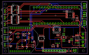
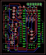
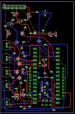
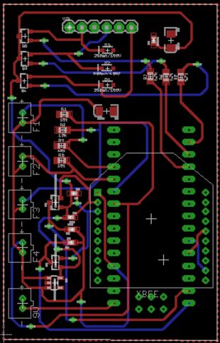
Foot PCB Schematic and Layout by Forest Nutter | Electronics and Control Engineer and David Mendoza | Manufacturing and Design Engineer:
First Iteration:
For the Layout of the Foot PCB, I took the schematic that was given to by Forest Nutter, the Electronics and Controls for the hand. Before I started laying out the Foot PCB, I had asked Forest to place certain components where he would like them at. Then I would place the, resistors, capacitors and transistors in what I thought were the best places. After routing everything and trying to hake everting connect and have 45 degree turns, I sent this, PCB Layout seen in Figure 1, to Fabian.
Fabian Replayed with:
Foot(1).brd
- Individual Traces should turn 45 degrees max. There are a lot of 90 degree turns on this one. 90 degree should only be used when joining a trace to another trace or starting the trace at an IC pad (see note below for Prosthetic PCB brd)
- I cant tell by looking, but make sure the pads of the surface mount ICs are a littler longer than the datasheet specifies so that you have an easier time hand soldering it. You want some extra copper to hit with the tip of the iron.
- Use CIRCLE, 0.019 inch vias
- Unused GPIO (D0, D1, D2…) and analog (A0, A1, A2…) should be tied to ground
- Do a ground copper pour on the bottom layer. Copper pour perimeter on top is skewed at the bottom right side.
Second Iteration:
After reading this I would go and make a few changes to the layout and more components around some more. Now every time I would run the DCR and see it there was any angle problem, clearance or overlaps, that caused be to move a routing line or component, I would then ripup the line and redraw it so that it still had the 45 degree angle. After I made these changes I would send the second version, shown in figure 2, to Fabian.
Fabian replied with:
Foot:
– only 45 degree angles (Use sparkfun drc(attached))
– round vias
– way to much wasted space
After reading this, I ripped up the routing lines connecting the components and moved them closer together to eliminate wasted space. Then before routing everything I made sure to change the vias setting to round with a .6 millimeter radius. As I was routing everything I made sure to only use the setting that would give me 45 degree angles. I would send Fabian the final version of the foot PCB layout, shown in figure 3.
[/av_textblock]
[av_toggle_container initial=’0′ mode=’accordion’ sort=”]
[av_toggle title=’Foot PCB Schematic’ tags=”]

[/av_toggle]
[av_toggle title=’Figure 1′ tags=”]
[/av_toggle]
[av_toggle title=’Figure 2′ tags=”]
[/av_toggle]
[av_toggle title=’Figure 3′ tags=”]

[/av_toggle]
[/av_toggle_container]
[av_hr class=’invisible’ height=’25’ shadow=’no-shadow’ position=’center’ custom_border=’av-border-thin’ custom_width=’50px’ custom_border_color=” custom_margin_top=’30px’ custom_margin_bottom=’30px’ icon_select=’yes’ custom_icon_color=” icon=’ue808′ font=’entypo-fontello’]
[av_heading heading=’Results’ tag=’h1′ style=’blockquote modern-quote’ size=’20’ subheading_active=” subheading_size=’15’ padding=’10’ color=” custom_font=”][/av_heading]
[av_textblock size=” font_color=” color=”]
After the third version was sent, I had received an email from Fabian that the PCB could have looked better but he approved of it to be shipped out and manufactured. Once the PCB came in, it was soldered and tested, the test failed, and the PCB did not work.
[/av_textblock]
[av_heading heading=’Conclusion’ tag=’h1′ style=’blockquote modern-quote’ size=’20’ subheading_active=” subheading_size=’15’ padding=’10’ color=” custom_font=”][/av_heading]
[av_textblock size=” font_color=” color=”]
Even though the PCB Layout was good enough to be approved by Fabian, it still should have been double checked by the E&C if there was any schematic problems. With the Layout part it is best to work together with the E&C in asking where they would like certain components to be placed and then optimize from there and move things as close as possible. Also make sure that there is still enough room to run the wires through with out and errors.
[/av_textblock]