Antenna Matching
Written by Zachary de Bruyn (Electronics & Control)
Table of Contents
Purpose
The PeteBot chassis team is unique in that it is utilizing two PCBs which operate on two different MCUs; the first being the heritage 3DoT v5.03 board which uses the ATMega32U4, and the second being the SAMB11, which incorporates the ATSAMB11. One significant different between the two boards is that the SAMB11 has a transceiver module. Because the SAMB11 can operate with the incorporated Bluetooth (BLE), an antenna network was needed to be designed to utilize the BLE transceiver. Because an antenna network was needed to be constructed with minimal input from the SAMB11 reference design, many steps were required to be performed in order to ensure that the SAMB11 could operate at the 2.4-GHz BLE frequency.
Antenna Selection
The first step in the overal process of incorporated a matching network is selecting a proper antenna based on the needs of the system. To reiterate, the operating frequency of BLE is 2.4-GHz. Along with frequency requirements, there are also size requirements. Our antenna therefore was required to operate at the BLE frequency, to be small enough to fit on a PCB, and to operate the PeteBot chassis. These requirements alone narrowed the possibilites of two types of antennas: PCB or chip antennas. With the PCB antennas, one antenna that looks promising is the meandered inverted-F antenna (MIFA). The chip antenna resembles a 0805 resistor or inductor. The two antennas are shown below:

Figure One – MIFA (Source: Cypress)
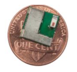
Figure Two – Chip Antenna (Source: Cypress)
Analyzing both types and data sheets of antennas, we discover that both antennas have an isotropic radiation pattern, meaning that the frequency of the antenna can be picked up equally from almost every direction. This is ideal for our applications due to the fact that the PeteBot will be required to operate via RC mode by an operated. A few other important antenna parameters are: return loss, gain, and bandwidth. Return loss is essentially how much of the power being transmitted is reflected due to the mismatch of the antenna’s imepdances. The standard for impedances is usually 50-Ohms. A return loss greater or equal to 10-dB is considered ideal for operation [1]. Referring to the following equaltion for return loss:

Equation (1)
At a return loss of 10-dB which translates to 90% of power transmittered going into the antenna, return loss of 20-dB translates to 99%. The gain is a measure of ow strong the radiation field is compared to the ideal omnidirectional antenna. For isotropic antennas, like that being applied to the PeteBot, gain is measured as dBi. The “i” simply indicates that the gain is measured frerence to an istropic antenna. While the MIFA antenna has a gain of about 5-dB depending on the plane of radation, the chip antenna has a peak gain of 0.5-dBi. The bandwidth requirements for the antennas requires that the BLE frequency is capable of interception, which was 2.4-GHz. The chip antenna has a frequency range of 2.4- to 2.5-GHz, which translates to a bandwidth of 100-MHz. The MIFA antenna operates a a comparable frequency range, and therefore has an equivalent bandwidth.
With comparable operational characteristics, an antenna selection for our purposes was based upon flexibility, in which the antenna can be used in a variety of configurations for the SAMB11 board. In the case of the PeteBot SAMB11 PCB, the chip antenna is the best candidate.
Matching Network
The purpose of an antenna matching network is to allow the most power to be delivered to the load. The load in the case of transcievers, like the SAMB11, is dependent on whether the antenna is transmitting or receiving. If the antenna is transmitting, then the antenna is the load, whicl the SoC SAMB11 is the load if the system is receiving. It is common practice to design a load with 50-Ohm impedences for RF traces [1]. As a review, the term impedance is mathematically defined as the magnitude of resistance and reactance. It is typically denoted by the letter “Z.”

Equation (2)
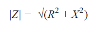
Equation (3)
In Equations (2) and (3), R denotes resistance, and X for reactance. Both values are measured in Ohms.
Now that impedance is defined and the typical characteristic impedance is defined as 50-Ohms, this information can be used in collaboration with the helpful tool called a Smith Chart.
Smith Chart
It is a graphicaly tool used to help plot complex impedances and used to define a matching network. It is also helpful in determining many important RF parameters, including VSWR, return loss, reflection coefficient, and transmission coefficients. Using this chart can design a matching network.

Figure Three – Smith Chart (Courtesy of Wikipedia)
There are a lot of reference towards using Smith charts on YouTube that will explain how to find the difference parameters.
The best usage of the Smith chart is to be able to measure the input impedances going into a load, where the input impedance is defined as Z_in. Character impedance is Z_0 and the load impedance is Z_L.
As an example, let’s say that the measured Z_in was 100-j100-Ohms. The first step would be to normalize the input impedance by dividing Z_in by Z_0, which would result in 2-j2-Ohms. This opint can be located on the Smith chart, and from this point (2-j2), you can use a combination of inductors and capacitors to move the impedance to the necessary location on the Smith chart, which is the center of the chart where the red dot is in Figure 3. The table below helps better understand how each component affects the impedance of the matching network.

Table One
Using any combination of passive elements can be used to get measured impedance as close as possible to the center of the Smith chart for optimal performance. If we refer to the matching newtorks in Figure 4 and Figure 5, we can see that the matching network consists of the passive elements described in Table One.

Figure Four – Chip Matching Network Antenna Reference Design

Figure Five – SAMB11 Matching Network Reference Design
Figure Five depicts the matching network reference design for the SAMB11 where the resistance network shown in the dotted square is omitted from the final design PCB. Also omitted was the capacitor laveld DNI (Do Not Include).
S-Parameters
Scattering parameters, or “S-parameters” are a set of parameters which define the electrical power delivered between two ports on a network, where a port is any where within the network containing voltage or current delivery [6]. The four parameters are displayed below:
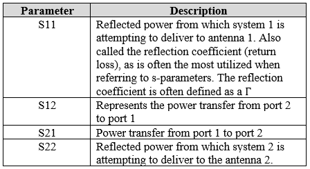
Table Two – S-Parameters
The reflection coefficient referred to in the S11 description is defined as followed:
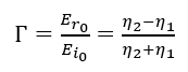
Equation Four – Reflection Coefficient
Where are the reflected and incident plane waves, and the is the intrinsic impedance of the medium the wave is traveling through, and is the intrinsic impedance of the surface/material medium the wave reflects or penetrates [5].
The S-parameters can be collected by using a Vector Network Analyzer, however they are fairly expensive, usually greater than $10,000 on the lower end models. As a substitute, there is software such as Microwave Office or Optenni which can calculate the S-parameters as well. While these software suites are NOT free, they do offer free “research” trials where you can use it free for a week (Microwave Office) or for a month (Optenni).
Optenni provides the most tutorials on how to get familiar with the basics of the software, and also offers an optimization tool which allows you to designate specific requirements you want for your design. For instance, in the case of the SAMB11 3DoTX board, the requirements for BLE is that it resonate at 2.4-GHz. By using Optenni, desired parameters can be chosen, and a matching circuit will be automatically constructed through the software. (Click Here, it will redirect you to the Optenni technical resource page).
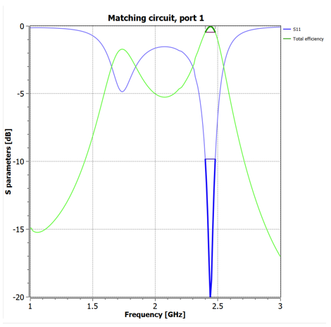
Figure Six – S11 Parameter
Example
As seen in the S parameter chart in figure 6, the S11 parameter extends just beyond -20-dB. The figure therefore suggests that at approximately -20-dB the antenna radiates at its maximum. At 0-dB the antenna radiates nothing. While this simulation may look ideal, it is not practical for real world application. This is because the dark blue highlighted bandwidth (2.4-2.483-GHz) is difficult to realize in the physical world. In practical antenna circuits, the resonating frequency an antenna could transmit/receive is always met with some percentage of error, or acceptable deviation from nominal conditions. For example, the chip antenna we have chosen for the 3DoTX board has a frequency range from 2.4 to 2.5-GHz. A 100-MHz difference. By choosing more than the two components that have been shown below, more components can be added to open up the bandwidth of frequencies that can be received/transmitted by the antenna. Another great feature with Optenni is that you can tune the component values to see how each one effects the S11 parameter.
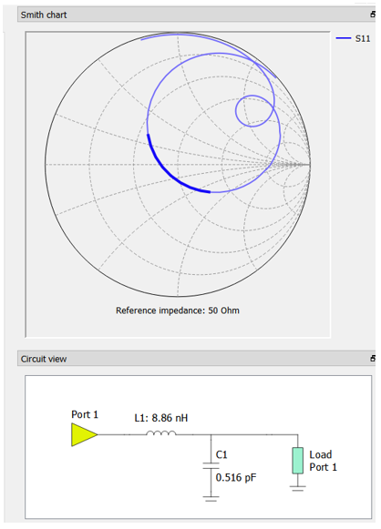
Figure Seven – Smith Chart (top) and matching generated circuit (bottom)
By looking at the smith chart in figure 7, we see that dark blue are highlighted on the graph corresponds with the dark blue area highlighted in figure 6. Recalling the information presented earlier about the smith chart and 50-Ohm impedances, we can see that the matching circuit accurately tunes the antenna to operate at the matched approximate 50-Ohm impedance.
In the matching circuit shown, the port corresponds with the input (i.e. the antenna) and the load corresponds with the SAMB11.
References
[1] Reference One
[2] Reference Two
[3] Reference Three
[4] Reference Four
[5] Fundamentals of Engineering Electromagnetics by David Cheng
[6] Reference Six
Acknowledgements
Thank you for Dr. Densmore, Dr. Rezvani, and Dr. Haggerty for help in contributing to understanding the matching network.