Sojourner F17: PCB Layout
By Malak Alamad (Design and Manufacturing) | Fall 2017 | Sojourner Team
(Updated 12/110/2017)
Introduction:
The PCB layout that we have for the Sojourner project is very similar to the design that last semester had. There were minor differences that were made from the previous design in order for it to fit our needs. If everything functions properly, the PCB’s function will be to drive the motors and to obtain a reading from the sensors.
Discussion:
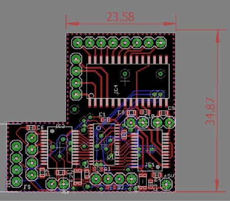
First, I needed to change the dimensions to ensure that the board fits into our chassis. I also had to change the orientation of one of the parts because the pins were in the wrong order. There were a few components that were placed outside of the boundaries of the board, so I had to find a placement for them and redo the traces. Redoing the traces became an immediate challenge because the traces that needed to be added had many other traces around them. It was difficult to find a path through both sides of the board that did not intersect with other traces. I also came across many errors while trying to finalize this design. The majority of the errors were either airwire errors or dimension errors. When shifting and adding components, some of the airwires were deleted. The board passed the 3Dot error check, but I also checked it against the Osh Park DRC and I had 200 dimension errors because many components were placed too closely to the edge of the board. I had to reposition many of the components in order to get everything to fit without experiencing any errors. An image of the layout is shown below.
Conclusion:
After everything was set in place, I ran the 3Dot DRC to check for any errors. I got rid of those and the PCB was set to be sent to Osh Park for fabrication after the customer’s approval.

