MicroDozer Fall 2019 – PCB IMU Design
Custom PCB Design with IMU
Author/s: Clare L.
Verification:
Approval:
Table of Contents
Introduction
A custom printed circuit board (PCB) was designed Fall 2019 for MicroDozer but can be used in many robots using the 3DoT board V9 [1] that need rotational orientation data or quadrature encoders. The orientation data comes from an inertial measurement unit (IMU), specifically the BNO055 designed by Bosch [2], for which Adafruit designed a breakout board [3]. The progression for the following steps will be shown: the physical breadboard setup, the PCB schematic in EAGLE, the PCB layout in EAGLE, and the completed board. Errors and preventative mistakes and suggestions for solutions are then outlined in the conclusion.
Breadboard Setup
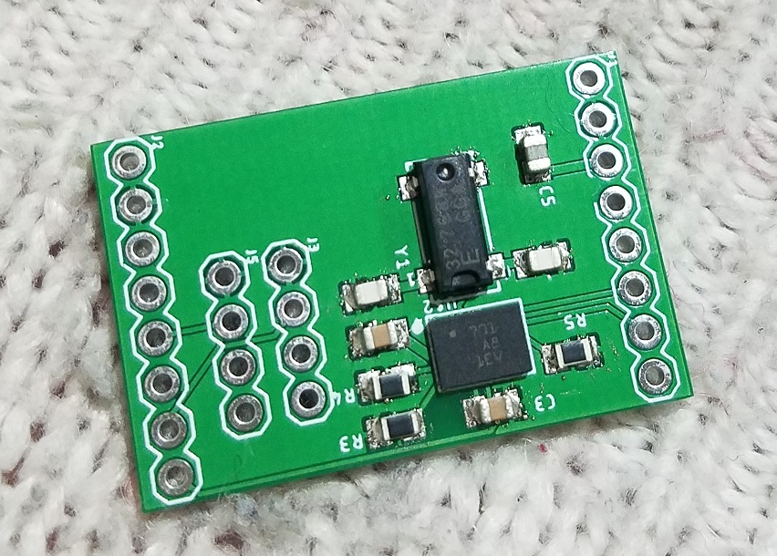
Bosch’s BNO055 IMU is an LGA (land gate array) package with 28 pins and a footprint of 3.8 x 5.2 mm2.
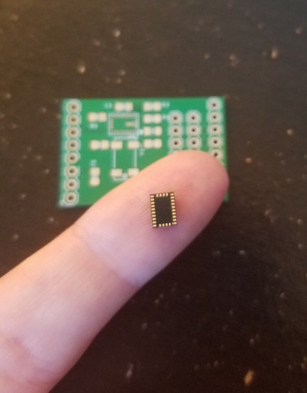
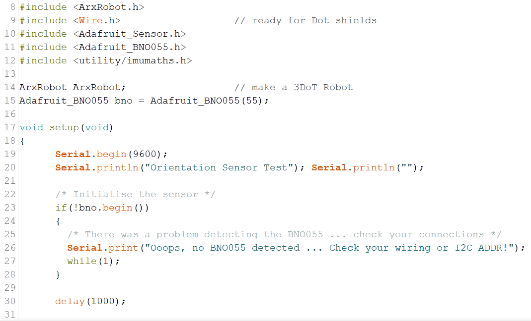
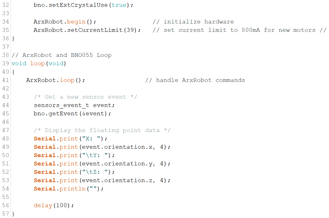
Because of the small size of the pins and the IMU itself, the breakout board from Adafruit was used to test compatibility with the V9 with the intention of using all components on the breakout board for the PCB. Only four pins on the board were needed: SDA, SCL, Vin, and GND. Vin from the breakout board was connected to 3.3V on the V9 – the simplicity of the hookup led to quick results. I2C readings were shown in the Arduino IDE in Euler angles in the x, y, and z directions with a code provided by Adafruit [4] combined with the ArxRobot_Basic code:
PCB Schematic
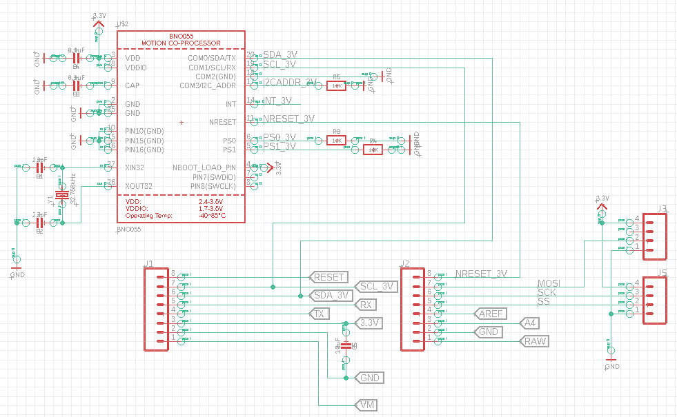
The EAGLE files (.brd and .sch) were available on GitHub [4]. The top left is the IMU, BNO055, which was largely unaltered. The crystal on the far left connected to the two capacitors was not giving much information inside of the EAGLE program itself. To narrow down which one it was, I opened up the .brd file inside of GitHub which can be read as a text file. Combing through it gave a hint as to which crystal it was, making it easier to find out which one to purchase.
The connectors J1 and J2 were long pin female header connectors that were eventually soldered to the top of the V9 board. SDA and SCL connections were made from the BNO055 to the connectors. Ideally, wires are drawn from components directly to the J connectors rather than renaming the pins on the J connectors, which can cause incorrect assignments.
The connectors J3 and J5 were for quadrature encoders. Quadrature encoders have two signals, but when working with dc motors, only one pwm signal for each motor was needed. Still, two pins were assigned for one quadrature encoder and one for another motor, for a total of three signals: MOSI, SCK, and SS. The connection SS was not available with the current version of the V9, but is expected to be available for this sort of assignment in a later version.
PCB Layout
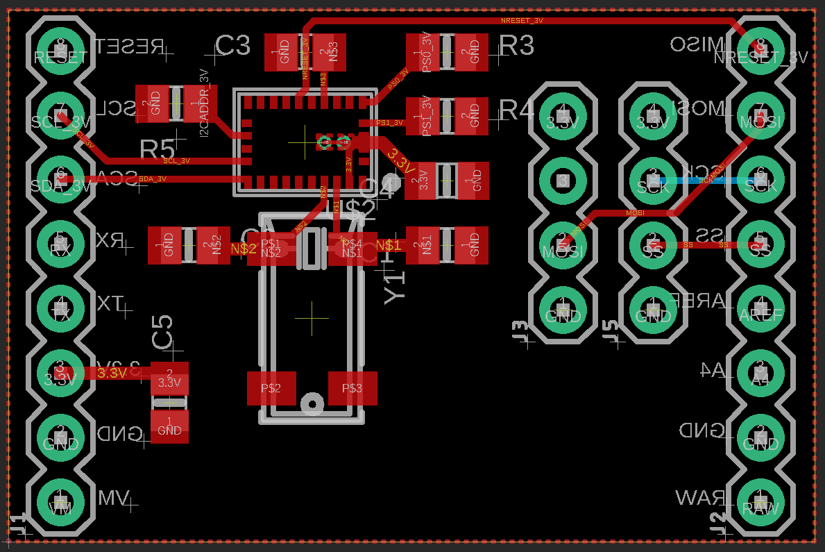
The connections on the left and right are 1×8 long pin female header connectors to make the PCB stackable. The labels for the pins are on the bottom of the PCB to make it easy to figure out how to orient it the right way on the V9.
The 2×4 connectors on the right are for the encoders: one motor can have one signal on MOSI and the other motor can have a signal on SCK. The bottom two connections on J3 and J5 are GND and the top two connections are 3.3V. A pool for ground was made on the entirety of the bottom layer of the PCB (save for any signals) and the top was a pool of 3.3V. As mentioned above, SS will be available for later versions of the 3DoT.
The signals in EAGLE were kept to width 10 minimum and power signals were a minimum of width 20.
The external crystal, near the middle of the board, was 32.768 kHz, 12.5 pF. There were a few complaints on Adafruit forums that the external crystal was effectively useless, but we wanted to include it anyway.
The passive components were as follows from bottom left, clockwise:
(1) 10 uF capacitor
(1) 22 pF capacitor
(1) 10k resistor
(1) 0.1 uF capacitor
(1) 10k resistor
(1) 10k resistor
(1) 0.1 uF capacitor
(1) 22 pF capacitor
Overall, the design took about 20 days, but I was lucky to have near-constant feedback and corrections from Hill maybe 15 times over that time.
Putting the PCB Together
To order tiny passive components like the capacitors and resistors, the footprint size needed to be found, which should be under the properties for each component:
For this capacitor, the footprint was 0805, which is size ….0.08″ x 0.05″. When I searched for 0805 capacitors or resistors on Digikey or Mouser, it was pretty easy to order from there.
Once the IMU, crystal, and passive components arrived, I applied the solder paste by hand. Always order a stencil! I thought stencils and reflow ovens were something optional, so I only ordered the PCB. Don’t do this!
Applying the solder paste was doable for the crystal, resistors and capacitors by hand, but pretty much impossible for the IMU. I didn’t know eyeballs could physically hurt until I tried applying solder paste to the PCB connections for the IMU.
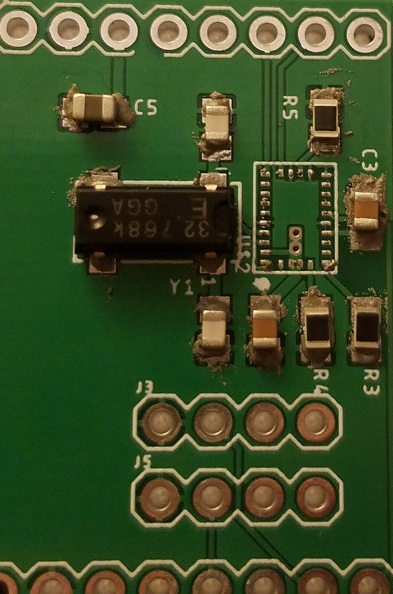
Not the final job, as the solder paste was cleaned up and squared around R4, C3, and C5, using a flat edged tool that wouldn’t cut or scrape the board. I also tried cleaning up the corners of the IMU connections, but had a feeling it was a lost cause. Ugh.
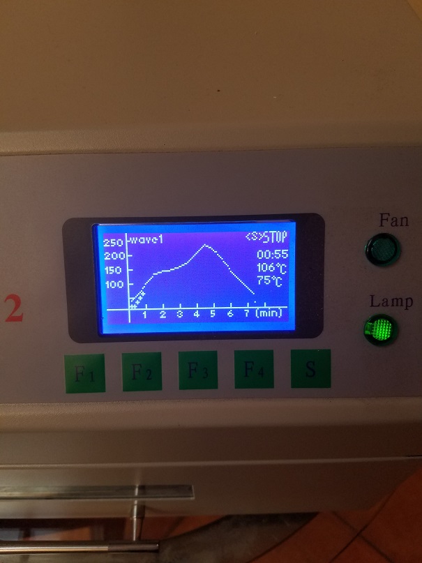
Next, the PCB was put into the reflow oven at Aosa. A student suggested I do it myself in a toaster oven, but I refused. The PCB needs to be heated with a specific thermal profile, with different stages of preheating, soak, reflow, and cooling. You can see the thermal profile in the second image:
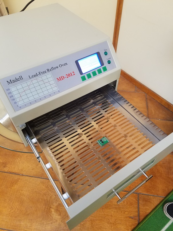
Overall, the baking took only about 7-8 minutes, with the result:
Next, was soldering on the header pins, which unfortunately, didn’t turn out well. Because the pins are only 2.5mm apart, a fine tip for soldering works best. I accidentally bought 2.0mm header pins and didn’t even check. Don’t do this either! I ended up with terrible quality header pins because I ordered some with the fastest shipping possible on Amazon too late in the semester.
Starting with the outer 1×8 rows, I knew I had some of the pins right when the solder quickly ‘pooled’ into the connection. Otherwise there were quite a few mishaps that could have been prevented with a much finer tip for soldering. The 1×4 header pins were short pin female headers.
Completed Board
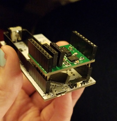
Finished PCB in the V9.
Conclusion
In the end, the PCB was not functional. The IMU needed to be placed with machine precision or someone with a very experienced hand as the solder paste likely got smeared during placement. Also, the soldering on the header pins needed more practice and could have been straighter. The 1×8 header pins also could have been better quality. When I realized I had ordered 2.0 mm spaced pins instead of pins that were 2.5 mm apart, I picked out ones that had the fastest shipping time and as a result, it lowered the quality of the PCB overall.