μDozer/Fall/2019
μDozer Custom PCB Design
Author/s: Deion Guillermo
Table of Contents
Introduction
In order for MicroDozer to utilize the additional components such as the ultrasonic sensor and IR sensor, a custom printed circuit board (PCB) was designed. Throughout the semester, this PCB evolves and changes are made as new components and challenges arise.
Iteration 1
Schematic
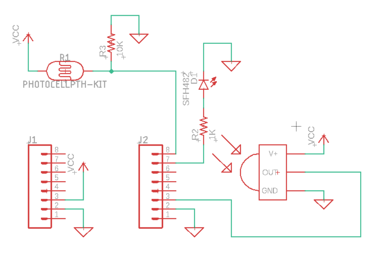
Figure 1: Iteration 1 Schematic
Board Layout
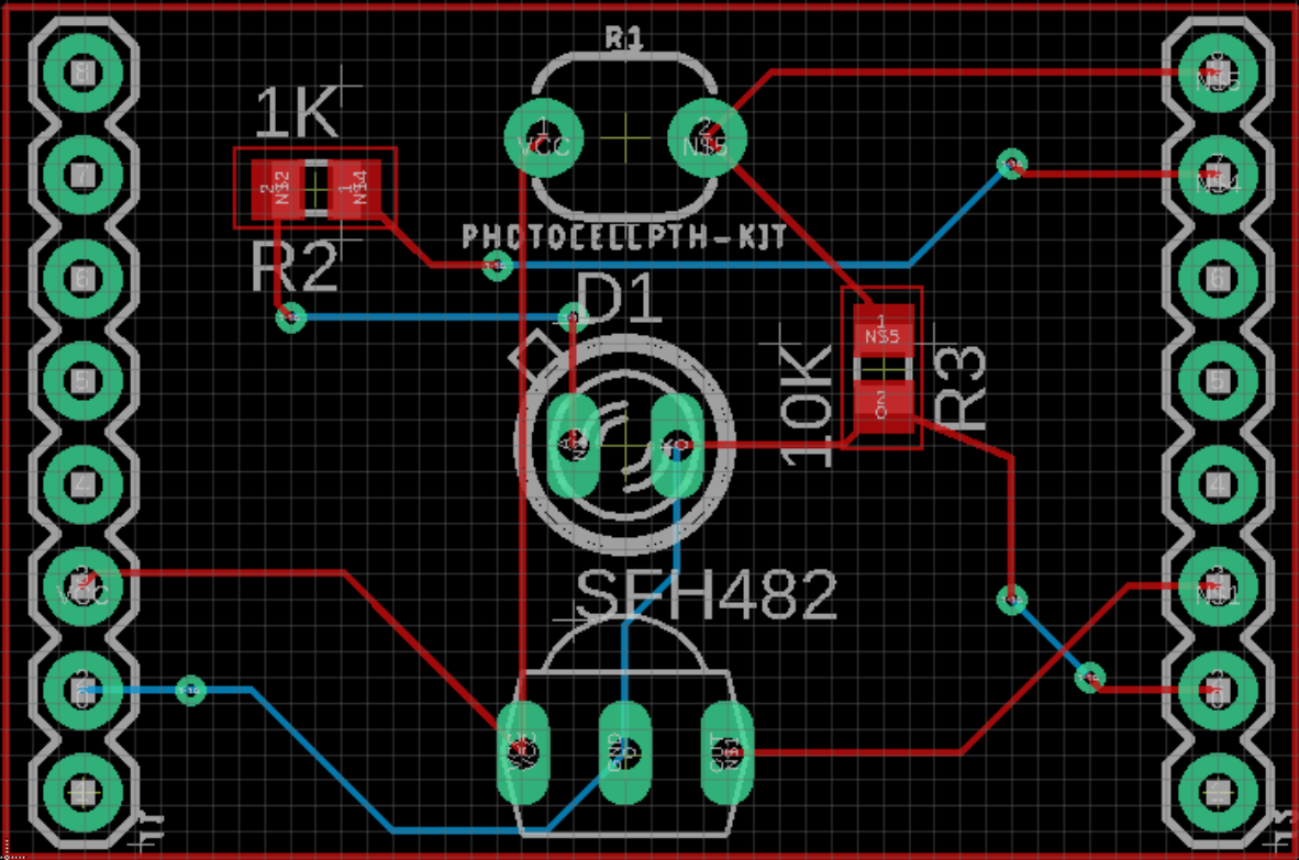
Figure 2: Iteration 1 Board Layout
This is the very first iteration of MicroDozer’s custom PCB. This version is extremely barebones, as it was our team’s first exposure to EagleCAD environment. As such, this iteration is riddled with a plethora of mistakes, such as extremely thin traces and poor routing with unnecessary vias. Many of these mistakes are addressed in the next iteration.
This iteration was mostly getting the correct parts and their corresponding EagleCAD files. Here, we use three main components for the Dozer: a photoresistor, an IR sensor, and an LED. Further, the 8-pin headers were also found within the Sparkfun Eagle Libraries.
Iteration 2
Schematic
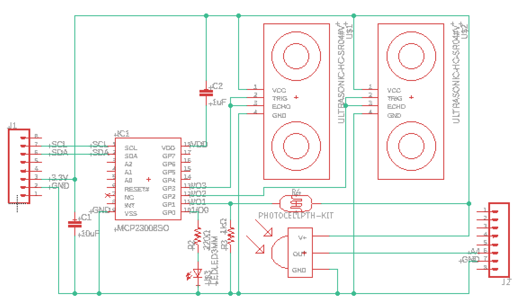
Figure 3: Iteration 2 Schematic
Board Layout
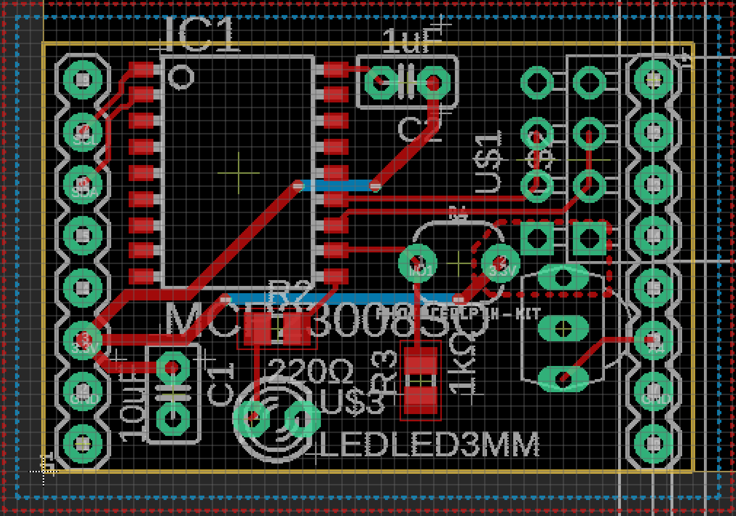
Figure 4: Iteration 2 Board Layout
At this point in the semester, many of the groups were scrambling to get their PCBs submitted and approved. Thankfully, the professor held two quick lectures addressing the common mistakes that others were making. Using those lectures as a guide, the next iteration of the MicroDozer’s PCB was improved.
Between the last iteration and this iteration, the team decided to include two ultrasonic sensors as seen in the top left of both the schematic and the board layout. With this inclusion, we also had competition for the pins available to use; We needed a pin for the LED, the photoresistor, the IR sensor and two ultrasonic sensors. The MCP23008 8-bit I/O expander is now included to accommodate for the large amount of pins needed.
First would be the schematic changes. Instead of connecting the sensors directly into the pins on J2, we now connect them into the I/O expander. The I/O expander now communicates to the board via the SCL and SDA pins found on the J1 header pins. From the lectures, the professor recommended to attach a 10μF decoupling capacitors between 3.3V power and GND. Further, any IC chip should also have this decoupling capacitor connected to power, albeit a smaller value such as .1μF. Another goal for the schematic is overall neatness; as we routed the schematic, we tried to keep intersecting nets to a minimum. In this particular iteration, the only intersections of wires are between wires that need to move up to power, or down to connect to GND. Last involves labelling, both removing and adding labels. There is a certain technique that one can utilize in EagleCAD where any net connected to a ground symbol will automatically be connected together. However, it is recommended to forego this technique and instead connect all GND nets together for example. Doing it this way can reduce the chance of improperly connecting wires together. Other pins on the board such as the SCL, SDA, 3.3V and GND pins are properly labeled on the schematic, and labels are reflected in the layout.
The layout also benefited from the small PCB lectures. With all the new components added, there was now a bit of competition for space on the board, but it was nothing too complex. To start off, the components were moved around the board and rotated around to reduce the amount of intersecting airwires. Using this layout method, this is how the power pins of the photoresistor, IR sensor, and ultrasonic sensors are all condensed into one area. Since all four of those pins were in the same general area, we decided to use a local pour in order to connect all four to power at using once power trace instead of wasting space for four. On the topic of power, the traces for these are 20 mils thick. We also followed the ‘star’ formation for the power traces. The reasoning for these power traces can be found on the Arxterra PCB tutorials. All the other traces that aren’t power traces were set to a thickness of 10 mils. Finally, many airwires/ traces were reduced by setting the top layer as a GND plane. In EagleCAD, this can automatically connect any airwires that needed to be connected to GND.
Even with these improvements, there were a couple issues that the team needed assistance in resolving. These issues came up as pins A0, A1, A2 and RESET# were not connected when the ERC was ran. While wanting to resolve these issues quickly and move forward with the project, the PCB was submitted alongside recommendations on how to resolve these issues.
Iteration 3
Schematic
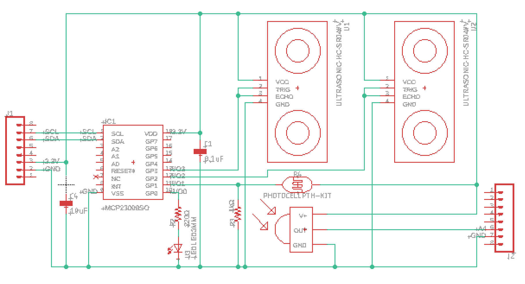
Figure 5: Iteration 3 Schematic
Board Layout
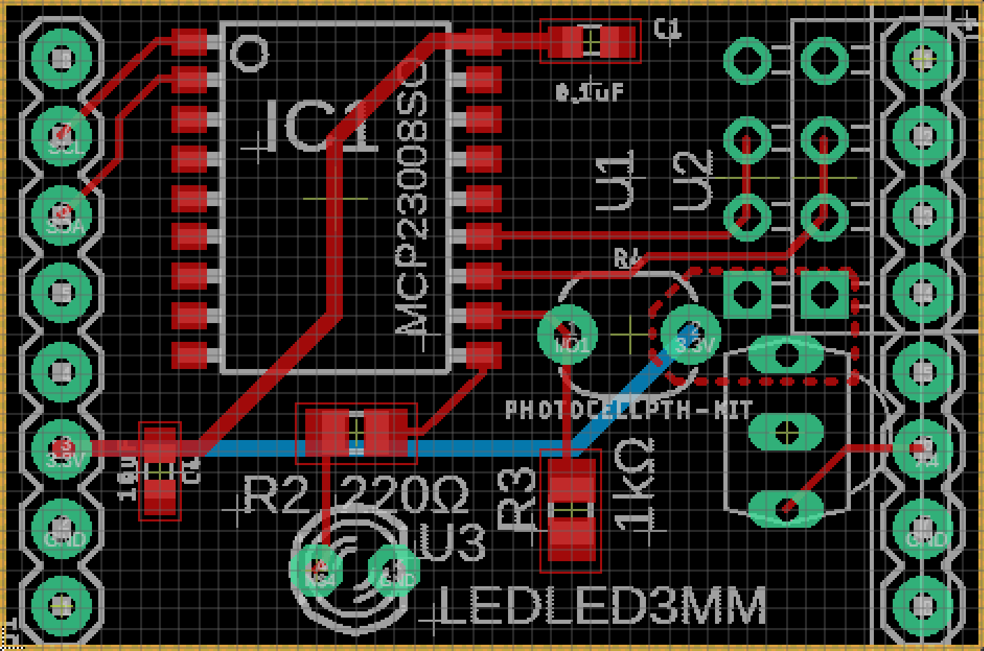
Figure 6: Iteration 3 Board Layout
This board is the next iteration edited by our wonderful professor. The changes here include a correction to the decoupling capacitor connected to the I/O expander. We misunderstood his lecture and connected a capacitor between the VDD pin on the I/O expander and 3.3V when it should instead be connected between power and GND. He also took the liberty of swapping out the capacitors to the 0603 SMD model, as we had used a different model previously. The labels on the second iteration’s board were also overlapping a bit, so their positions were adjusted to be more readable. Lastly, the professor gave advice to look up whether the ultrasonic sensors also require a decoupling capacitor as well as guidance on how to resolve the ERC errors from the previous iteration.
Iteration 4
Schematic
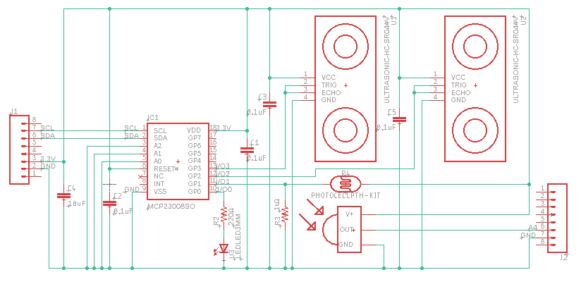
Figure 7: Iteration 4 Schematic
Board Layout
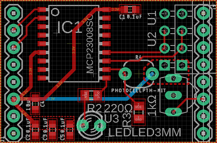
Figure 8: Iteration 4 Board Layout
This iteration takes the advice from the professor and applies it to this new schematic. First, it resolves most of the ERC errors by connecting the A0, A1, and A2 pins to ground, making the address of these input pins 000, as seen from the datasheet. Also, since the reset pin is active LOW, it is pulled high and connected to power. Lastly more decoupling capacitors are added, each for the reset pin and the two ultrasonic sensors. The capacitors for the ultrasonic sensors aren’t completely necessary, but they do reduce noise such that the signals are slightly cleaner. For the board layout, not much changes from the previous iteration. Two power traces are added that connect to the reset pin and the new decoupling capacitors. These capacitors are connected in another local pour to reduce the power traces needed for all three to only one trace.
Iteration 5
Schematic
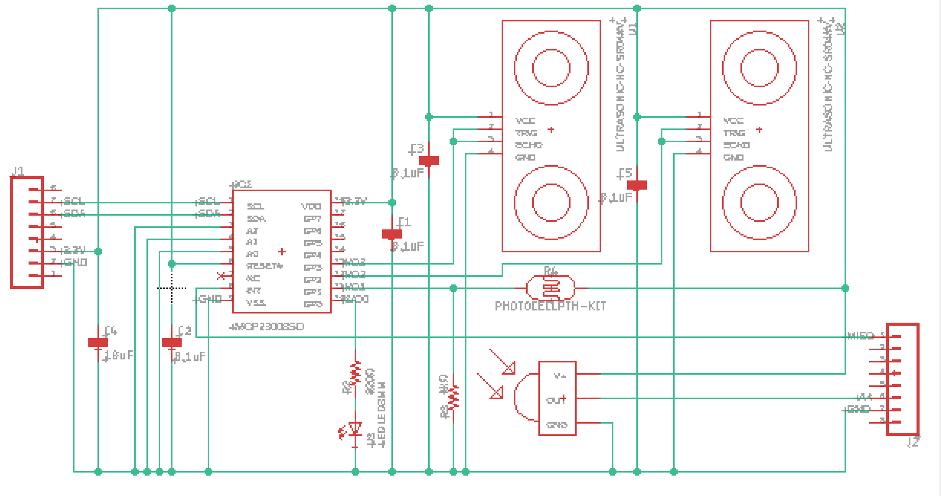
Figure 9: Iteration 5 Schematic
Board Layout
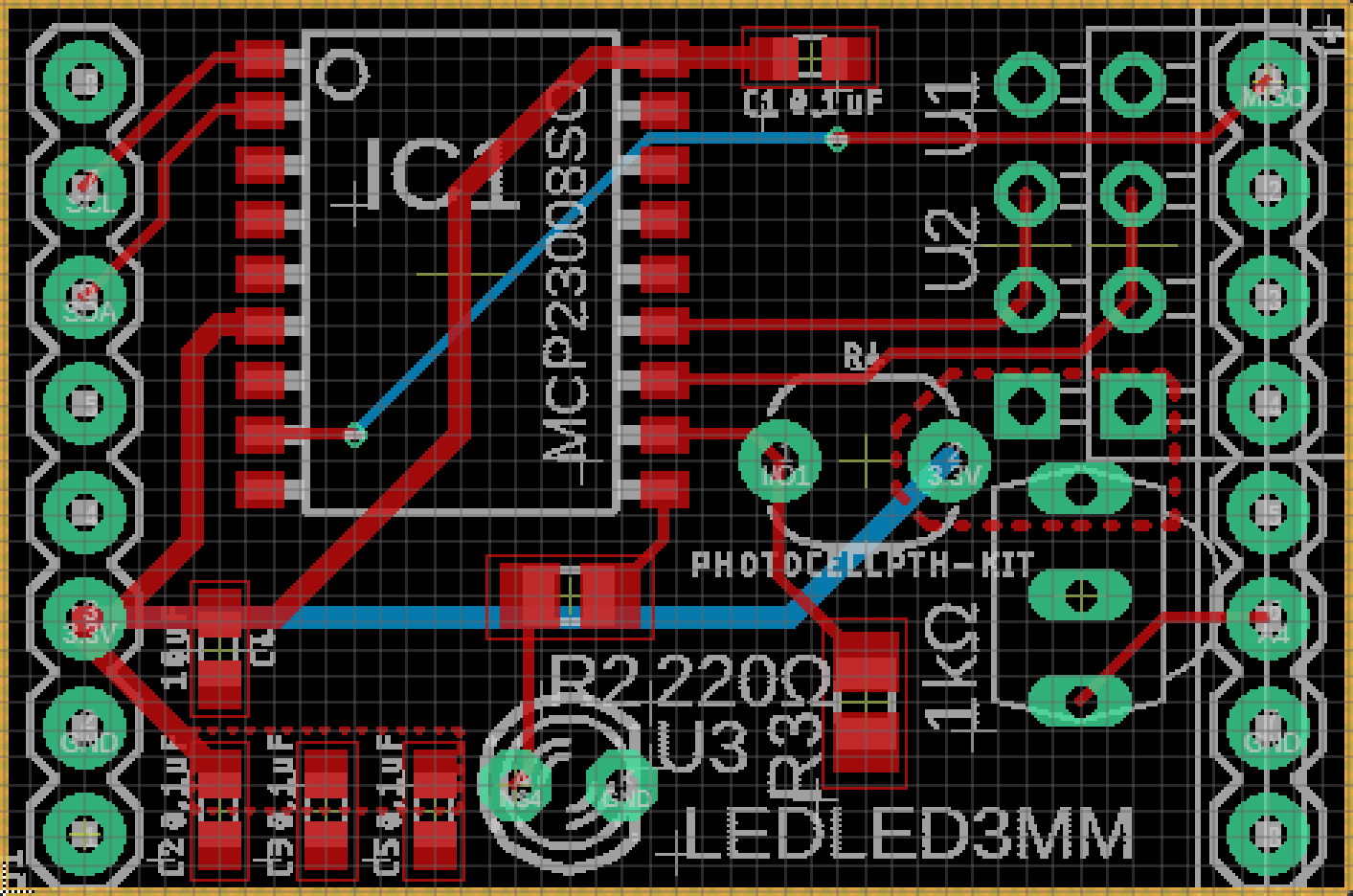
Figure 10: Iteration 5 Board Layout
This last iteration merely adds a single trace, connecting the interrupt pin to the MISO pin. At the time of making this schematic, we are unsure if interrupts are necessary for the robot. However, this trace was added in case we actually decide to utilize it, under the recommendation of our professor. This PCB was approved to be manufactured by the professor. The PCB was ordered on December 2, 2019 and delivered by December 5, 2019.
Conclusion
In all, the process to design and manufacture a custom PCB is an iterative process. By communicating back and forth between the professor, this PCB was able to improve with each new iteration.