Working with Bits and Bytes: Logic Instructions and Programs
READING
The AVR Microcontroller and Embedded Systems using Assembly and C
by Muhammad Ali Mazidi, Sarmad Naimi, and Sepehr Naimi
Sections: 5.3, 5.4, 5.5
Table of Contents
OVERVIEW
Clearing and Setting a Bit In …
| Where | Instruction | Alternative | Notes |
|---|---|---|---|
| I/O (0 – 31) | cbi, sbi | Use with I/O Ports | |
| SREG | cl{i,t,h,s,v,n,z,c}
se{i,t,h,s,v,n,z,c} |
bclr
bset |
|
| Working with General Purpose Register Bits | |||
| Clearing and Setting a Byte | clr, ser | ||
| Clearing Bits | and, cbr | andi | |
| Testing Bits | and | Also consider using sbrc, sbrs, sbic, sbis (see Control Transfer Lecture) | |
| Testing a Bit | bst |
||
| Testing a Byte | tst |
||
| Setting Bits | or, sbr | ori | |
| Inserting a Bit Pattern | cbr |
and |
|
| Complementing (Toggling) Bits | eor | ||
| Rotating Bits | rol, ror | ||
| Shifting Bits | lsl, lsr, asr | ||
| Swapping Nibbles | swap | ||
SAMPLE APPLICATION – KNIGHT RIDER
KnightRider:
; See page 5 and 6 – Clearing and Setting Bits
clr r16 // start with r9 bit 6 set – LED 6
sbr r16, 0b10000000
; Q1: How could we have done this using 1 instruction?
ldi r17,(1<<sreg_t) equivalent=”” to=”” 0b01000000<=”” span=””></sreg_t)>
; See page 7 – Clearing and Setting a Bit in the AVR Status Register
clt // initialize T = 0, scan right
; See page 8 – Testing Bits
loop:
ldi r19, 0b100000001
and r19,r16 // test if LED hit is at an edge
breq contScan // continue scan if z = 0
; See page 9 – Toggling Bits
in r16,SREG // toggle T bit
eor r16, r17
out SREG,r16
; See page 10 – Rotating and Shifting Bits
contScan:
brts scanLeft // rotate right or left
lsr r16
rjmp cont
scanLeft:
lsl r16
cont:
mov spiLEDS, r16
call WriteDisplay
rcall Delay
rjmp loop
SAMPLE APPLICATION – BICYCLE LIGHT
A bicycle light has 5 LEDs.
BicycleLight1: A repeating pattern starts with the center LED turned ON. The center LED is then turned OFF, and the LEDs to the left and right of the center LED are turned ON. Each LED continues its scan to the left or right. Once the LEDs reach the end the pattern repeats itself. Using the CSULB shield, write a program to simulate this bicycle light.
BicycleLight2: Same as Bicycle1 except when LEDs reach the edge, they scan back to the center.
BicycleLight1:
clr r7 // turn off 7 segment
begin: ldi r16, 0x04 // scan register r16 = 4
mov r17, r16 // scan register r17 = 4
scan: mov r8, r16 // do not modify r16
cbr r17, 0x20 // r17 bit 5 = 1 at end of cycle
or r8, r17 // combine scan registers
rcall Delay
call WriteDisplay
lsr r16 // scan r16 right
lsl r17 // scan r17 left, r17 = 0 at end of cycle
brne scan // if r17 <> 0 then continue scan
rjmp begin // else start next cycle
BicycleLight2:
ldi r16, 0x08 // 000|0_1000 start just in from edges
ldi r17, 0x02 // 000|0_0010
scan: mov r8, r16
or r8, r17
rcall Delay
call WriteDisplay
lsl r17 // scan r17 left
lsr r16 // scan r16 right
brcc scan
rjmp BicycleLight2
CLEARING BITS
To clear a bit set the corresponding mask bit to 0
and source/dest register, mask register
Problem: Convert numeric ASCII value (‘0’ – ‘9’) to its
binary coded decimal (BCD) equivalent (0 – 9).
- What we have: ‘0’ to ‘9’ which equals 3016 to 3916
- What we want: 0 to 9 which equals 0016 to 0916
Solution: Mask out high-order nibble
lds r16, ascii_value
ldi r17, 0x0F
and r16, r17 // or simply andi
sts bcd_value, r16
An alternative to the and instruction is the Clear Bits in Register cbr instruction.
cbr source/dest register, mask bits
The cbr instruction clears the specified bits in the source/Destination Register (Rd). It performs the logical AND between the contents of register Rd and the complement of the constant mask (K). The result will be placed in register Rd.
Rd Rd ∙ (0xFF – K)
Here is how the previous problem would be solved using the cbr instruction.
lds r16, ascii_value
cbr r16, 0xF0
sts bcd_value, r16
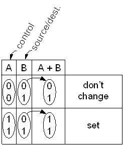
SETTING BITS
To set a bit set the corresponding mask bit to 0
or source/dest register, control register
Example: Set to one (1) bits 4 and 2 in some port.
in r16, some_port
ldi r17, 0b00010100
or r16, r17 // or simply ori
out some_port, r16
An alternative to the or instruction is the Set Bits in Register sbr instruction.
sbr source/dest register, mask bits
The sbr instruction sets the specified bits in the source/Destination Register (Rd). It performs the logical ORI between the contents of register Rd and the constant control (K). The result will be placed in register Rd.
Rd Rd + K
Here is how the previous problem would be solved using the cbr instruction.
in r16, some_port
sbr r16, 0b00010100
out some_port, r16
CLEARING AND SETTING A BIT IN THE AVR STATUS REGISTER
AVR Instructions for Clearing and Setting SREG bits
cl{i,t,h,s,v,n,z,c} or bclr SREG_{I,T,H,S,V,N,Z,C} // defined in m328Pdef.inc
se{i,t,h,s,v,n,z,c} or bset SREG_{I,T,H,S,V,N,Z,C} // defined in m328Pdef.inc
Examples:
Disable all Interrupts
cli
Set T bit
set
TESTING BITS
Use the andi instruction to test if more than one bit is set
andi source/dest register, mask bits
Example 1: Branch if bit 7 or bit 0 is set
// 7654 3210
lds r16, some_bits // 1000 0000 example
andi r16, 0b10000001 // 1000 0001
brbc SREG_Z, bit_set // 1000 0000 (alt. brne)
Example 2: Branch if bit 4 and bit 2 are clear
// 7654 3210
lds r16, some_bits // 1101 1001 example
andi r16, 0b00010100 // 0001 0100
brbs SREG_Z, bits_zero // 0001 0000 (alt. breq)
Consider using one of the “Skip if Bit” instructions if you only need to test one bit.
Review “Control Transfer” lecture material for details.
Use the tst instructions to test if a register is Zero or Minus.
Tests if a register is zero or negative. Performs a logical AND between a register and itself. The register will remain
unchanged.
Example: Branch if bear is in the forest
rcall inForest // returns false(r24 = 0) if bear is not in the forest
tst r24
breq not_in_forest // branch if r24 = 0
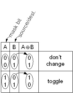
TOGGLING BITS
To toggle (complement) a bit set the corresponding mask bit to 1
eor source/dest register, mask register
Example: Toggle bits 5 and 3 of I/O-Port D.
//7654 3210
in r16, PORTD // 1101 1001 example
ldi r17, 0x28 // 0010 1000
eor r16, r17 // 1111 0001
out PORTD, r16
When toggling an I/O-Port bit, consider writing a one to the corresponding pin.
Review “AVR Peripherals” lecture material for details.
Example: Toggle bits 5 and 3 of I/O-Port D.
sbi PIND, PIND5 // equivalent to sbi 0x09, 5
sbi PIND, PIND3
When toggling a byte (8 bits), use the Complement instruction.
Example: Write TurnAround code snip-it (i.e., toggle SRAM variable dir)
// 7654 3210
lds r16, dir // 1101 1001 facing East
com r16 //_____ 0010 0110 facing West
cbr r16, 0xFC //1111 1100 clear unused bits (optional)
sts dir, r16 // 0000 0010
Question: How could you have complemented dir without modifying the other 6 bits?
ROTATING AND SHIFTING BITS
Rotate Instructions allow us to rearrange bits without losing information and to sequentially test bit (brcc, brcs). Shift instructions allow us to quickly multiply and/or divide signed and/or unsigned numbers by 2.
Rotate Left through Carry
rol Rd
Shifts all bits in Rd one place to the left. The C Flag is shifted into bit 0 of Rd. Bit 7 is shifted into the C Flag. This operation, combined with LSL, effectively multiplies multi-byte signed and unsigned values by two.
Rotate Right through Carry
ror Rd
Shifts all bits in Rd one place to the right. The C Flag is shifted into bit 7 of Rd. Bit 0 is shifted into the C Flag. This operation, combined with ASR, effectively divides multi-byte signed values by two. Combined with LSR it effectively divides multibyte unsigned values by two. The Carry Flag can be used to round the result.
Logical Shift Left (Arithmetic Shift Left)
lsl Rd
Shifts all bits in Rd one place to the left. Bit 0 is cleared. Bit 7 is loaded into the C Flag of the SREG. This operation effectively multiplies signed and unsigned values by two.
Logical Shift Right
lsr Rd
Shifts all bits in Rd one place to the right. Bit 7 is cleared. Bit 0 is loaded into the C Flag of the SREG. This operation effectively divides an unsigned value by two. The C Flag can be used to round the result.
Arithmetic Shift Right
asr Rd
Shifts all bits in Rd one place to the right. Bit 7 is held constant. Bit 0 is loaded into the C Flag of the SREG. This operation effectively divides a signed value by two without changing its sign. The Carry Flag can be used to round the result.
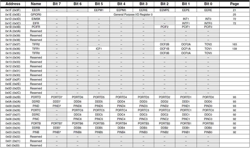
CLEARING AND SETTING A BIT IN ONE OF THE FIRST 32 I/O REGISTERS
Example: Pulse Clock input of Proto-Shield Debounce D Flip-flop (PORTD5). Assume currently at logic 0.
sbi PORTD, 5
cbi PORTD, 5
SETTING A BIT PATTERN
Use the Clear Bits in Register cbr or functionally equivalent andi instruction in combination with the Set Bits in Register sbr to set a bit pattern in a register.
Problem: Convert a binary coded decimal (BCD) (0 – 9) number to its ASCII equivalent value (‘0’ – ‘9’).
- What we have: 0 to 9 which equals X016 to X916
The X indicates that we do not know what is contained in this nibble. - What we want: ‘0’ to ‘9’ which equals 3016 to 3916
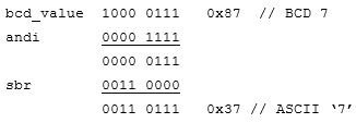
Solution: Set high-order nibble to 316
lds r16, bcd_value
andi r16, 0x0F // clear most significant nibble
sbr r16, 0x30 // set bits 5 and 4
sts ascii_value, r16
What is Happening
QUESTIONS
- What instruction is used to divide a signed number by 2?
- What instruction is used to multiply an unsigned number by 2?
- What instruction(s) would be used to convert a word pointer into a byte pointer? A word pointer is a register pair like Z containing the address of a 16-bit data (2 byte) word in an SRAM Table. A byte pointer is a register pair like Z containing the address of an 8-bit data byte in a corresponding SRAM Table. Assuming there is a one-to-one relationship between each word in the first table with a byte in the second table. And remembering that SRAM is always addressed at the Byte level, how would convert a pointer defined for the word table into a pointer defined for the byte table.
Appendix
APPENDIX A: KNIGHT RIDER OPTIMIZED
.INCLUDE
rjmp reset
.INCLUDE “spi_shield.inc”
reset:
call InitShield
// initialize knight rider
ldi r16, 0b10000000 // start with r9 bit 7 set – LED 7
mov spiLEDS, r16
// initialize roulette
ldi r19,0xE0
ldi r20,0x1F
ldi r16,0x01
mov spi7SEG,r16
loop:
// night rider routine
ldi r16, 0b10000001
and r16, spiLEDS // test if LED hit is at an edge
breq contScan // continue scan if z = 0
bst spiLEDS, 0 // if right LED ON, then T = 1
contScan:
brts scanLeft // rotate right or left
lsr spiLEDS
rjmp cont
scanLeft:
lsl spiLEDS
cont:
// roulette routine
add spi7SEG, r19
and spi7SEG, r20
rol spi7SEG
rcall WriteDisplay
rcall Delay
// display routine
rcall WriteDisplay
rcall Delay
rjmp loop
APPENDIX B: KNIGHT RIDER ADDRESSING INDIRECT
begin:
ldi r16, 14 // loop 14 times
ldi ZH, high(Table<<1) // set base address
ldi ZL, low(Table<<1)
scan:
lpm r9, Z+ // load constant to LED display register
rcall WriteDisplay // display routine
rcall Delay
dec r16
brne scan // if r17 <> 0 then continue scan
rjmp begin // else start next cycle
KnightRider: .DB 0x80, 0x40, 0x20, 0x10, 0x08, 0x04, 0x02
.DB 0x01, 0x02, 0x04, 0x08, 0x10, 0x20, 0x40
Knight Rider Dual Scan
ldi r18, 0x01
clr r19
ldi r20, 0b10000001
loop:
lsl r18
lsr r19
mov r8, r18
or r8, r19
rcall Delay
rcall WriteDisplay
and r8, r20
breq loop
push r18
push r19
pop r18
pop r19
rjmp loop
BICYCLE LIGHT SOLUTION BY ARTHUR KU FALL 2017
The idea behind this one is that the different numerical states of our LEDs have a difference from their neighbors by +6,+7,-7,-6 repeating, and so I can use the half-carry to decide when to toggle r16.
BicycleLight4:
ldi r16, 0x0A
mov r8, r16
ldi r16, 0x06
scan4:
inc r16
add r8, r16
rcall WriteDisplay
rcall Delay
brhc scan 4
com r16
rjmp scan4


