Goliath Spring 2018 – Custom Shield Layout
By: Milton Ramirez (E&C Engineer)
Verified By: Ernie Trujillo (Project Manager)
Approved By: Miguel Garcia (Quality Assurance)
Table of Contents
Introduction
This blog post will go over all the different iterations for the PCB layout for Goliath.
Eagle Layouts
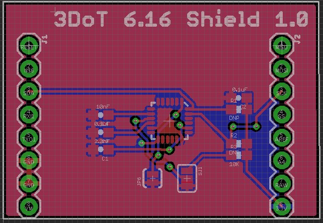
This design was just a rework of the ITG-2200 breakout, to fit on top of the 3DoT board. All the capacitors and resistors are connected to ground and are paired together so that it could look nice. Same goes for all of the capacitors and resistors connected to voltage source 3.3V. This layout is also using an old set of pins that have SCL on the right side of the connectors and SDA on the left side. The top layer is connected to ground while the bottom layer is connected to 3.3V
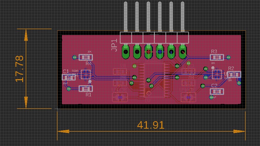
This board connects two UV sensors to a multiplexer, which connects to the SDA and SCL of the 3Dot board. The multiplexer is on the bottom layer of the board. This was done to make space on the top layer. All the resistors that were connected to their respective part were placed together. For example, resistors R1, R4, and capacitor C1 are placed next to U4. The six pins were placed on top so they can connect to the six pins on the bottom of the 3dot. This was an earlier design of the 3dot since the new 3dot has 8 pins now. Same as the gyro, which the top layer is connected to ground and bottom is connected to 3.3V.
The final layout combines the previous two layouts. In this layout, the connectors on top are for the path-finder breakout board. The connectors on the side are the so that our PCB can be mounted on top of the 3dot board. The UV sensors are spaced at 1.7cm. The LEDs are both placed under the UV sensors so that the best possible readings from the UV sensors can be obtained. The capacitors C1, C2, and C5 are all coupling capacitors and are placed as close as possible to the voltage pins of the two UVs and Gyro. The I2C expander from the previous design was replaced with the 2 address I2C multiplexer PCA9540BDP. The pull-up resistors, the range-finder connectors, Gyro and I2C share were replaced with a resistor array to make more space on the top left side. This helped because the SDA and SCL pins are on the top left side and needed as much space as possible since the I2C, Gyro, and range-finder are all connected to those same pins. The top layer of the PCB is grounded while the bottom layer is connected to the voltage source 3.3V.
These next two figures are earlier designs of the final design since this is the version that went through many iterations.
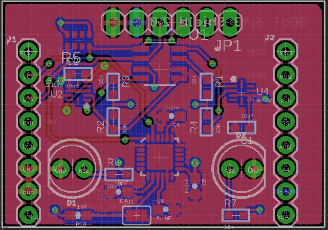
This circuit used an 8 address multiplexer and had a set of pull-up resistors for both the multiplexer and gyro. The coupling capacitors are also not where they’re supposed to be. Also, this design was still using the 8 address I2C. Since this chip was big, it was placed in the bottom layer to make space for the rest of the parts. The LED’s are also missing in this iteration.
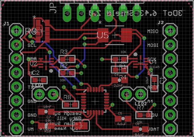
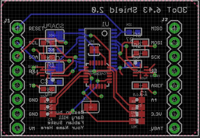
Figure 5. Another iteration that was closer to the final design. One notable difference from this design is that I tried to use connectors for the LEDs. This iteration has the 2 address I2C and the resistor array added.
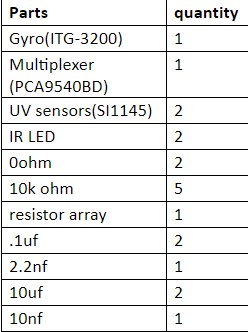
Parts Required
Conclusion
The PCB was approved April 21, 2018. Was ordered on April 26, 2018, and will arrive May 5, 2018.
References
- https://www.sparkfun.com/products/11977
- https://www.digikey.com/product-detail/en/nxp-usa-inc/PCA9540BD118/568-1844-1-ND/789976
- https://www.adafruit.com/product/1981
- https://www.adafruit.com/product/2717?gclid=CjwKCAjwlcXXBRBhEiwApfHGTd0vBvwKsP8KS7RMRyuV4j720AR6SxzWgmhaRgt9JazlS-hEpLF4HhoCSbQQAvD_BwE

