PCB Layout Design and Guidelines
Table of Contents
Tutorials
IMPORTANT: This document is designed to complement NOT replace these tutorials.
These tutorials use Eagle GUI, an alternative is the command line. You can find a list of these commands here.
SparkFun
Nate SMD Series
Jimbo Through-hole Series
Another (earlier) tutorial by Nate
Better PCBs in Eagle by Nate
Really Nice
On the Web
Source Documents
Graphical User Interface (GUI) Elements
Layers
- Using EAGLE: Board Layout https://learn.sparkfun.com/tutorials/using-eagle-board-layout
- EAGLE CAD layers reference http://www.element14.com/community/servlet/JiveServlet/download/74276-111817/eagle-cad-layers-reference3.pdf
- An Introduction to Layers in Eagle
https://learn.adafruit.com/ktowns-ultimate-creating-parts-in-eagle-tutorial/creating-a-package-outline
To turn any layer off or on, click the “Layer Settings…” button – – and then click a layer’s number to select or de-select it. Before you start routing, make sure the layers above (aside from tStop and bStop) are visible. Source: https://learn.sparkfun.com/tutorials/using-eagle-board-layout
Tip: Click-Drag to quickly turn on and off multiple layers
Layer Preset Views
Setup layers you want to give a name to (for example Final view). Right-click layer menu item and select New and Save.
PCB Legend
The PCB legend is white text that can be printed onto the PCB. This is useful for showing where the components will be placed, and also the identifier (resistor R1, R2 etc) or component value (the default CAM processor settings don’t print the component value). Layers shown highlighted in green with white letters.
Look for Interference:
- This view show where solder mask will not be applied. This includes vias which could result in a short if too close
18 Visa, 29 tStop
This is not the case with SparkFun Pro_Micro board.
- This view shows where board and parts overlap
20 Dimension, 21 tPlace, 25 tName, 29 tStop, 31 tCream, 39 tKeepout, 51 tDoc Outline of Parts
Blank on PaperBot PCB
1 Top
16 Bottom
17 Pads
18 Vias
19 Unrouted
20 Dimensions – the outline of the board
21 tPlace – The top silkscreen layer is used to draw text/lines/shapes on your PCB. Some symbols show the tPlace legend trampling over the SMD pad, but the manufacturer will automatically override this because of the tStop layer
22 bPlace
23 tOrigin
24 bOrigin
25 tName
26 bName
27 tValues
28 bValues
29 tStop
30 bStop
31 tCream
32 bCream
33 tFinish
34 bFinish
35 tGlue – shows glue for discrete components
36 bGlue
37 tTest
38 bTest
39 tKeepout – banned area for component placement. There is also a vRestrict layer for vias (banned area for vias).
40 bKeepout
41 tRestrict – banned area for tracks (currently none defined)
42 bRestrict
43 vRestrict — banned area for vias (currently none defined)
44 Drills
45 Holes – Holes can also be placed directly on the circuit board. When a hole is placed, it can be seen by viewing the Holes layer. Note that there are different symbols for different sized holes, so visually on the screen you may see a different shape from the one in this example. Regardless of the symbol on the screen, the final drilled hole is the same of course, it is just a hole. (Reference 1 page 3 “Holes”)
46 Milling
47 Measure – my dimensional notes
48 Document
49 Reference – on my drawing USB outline is shown (see 21 tPlace) and two diagonal lines probably related to IC since dislocated. Cannot manually delete these lines – Delete Layer?
50 dxf
51 tDoc – The tDocu layer is generally a useless layer. It is not part of the PCB or the legend, so the fact that it is trampling the pad can always be safely ignored. The tDocu layer is used only when documentation is printed, to show where the component goes.
52 – 255 except 210bmp-32U4 are blank
Layer Manipulation
Cadsoft EagleCAD Tutorial – Layer Manipulation. This starts from the circuit and board created in the 12 Lesson Project Board. He has made a surface mount version of the Project Board. This tutorial goes over the layers and what they show.
How to create a custom view of the final board
Start 6 minutes into the video. Turn on the  plus the
 ![]() views. Right click layer icon
views. Right click layer icon ![]() and select New. Enter “Final.” From now on when you just want to see the way the PCB will look simply right click and select Final. Do not forget to click on the rats nest icon
and select New. Enter “Final.” From now on when you just want to see the way the PCB will look simply right click and select Final. Do not forget to click on the rats nest icon ![]() to see the ground plane. Also how to setup top cream layers view.
to see the ground plane. Also how to setup top cream layers view.
29 tStop, 30 bStop – pads for through-hole parts plus holes
31 tCream, 32 bCream – Solder paste stencil
Overview of the process
Instructions on how to accomplish each step are in the tutorials and “Guidelines and How To” section.
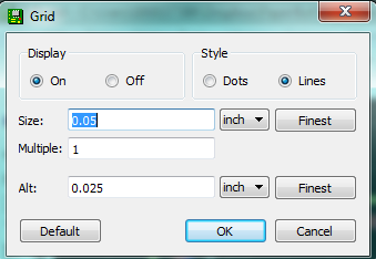
- Set grid to default with grid on.
- Draw border on Dimension Layer
- Turn off ground air wires
- CTRL-Click with move tool to snap parts to grid
- Move and rotate parts to minimize crossing air-wires. You may want to extend parts temporarily outside border to help you untangle the air wire (Lawrence Tip). Use ratsnest tool often to update air wires.
- You may also want to use the autorouter to have Eagle help you see what needs to be done. When you are done, use “group rip-up” to restore air wires.
- Add ground plane to top and bottom layer – multipoint ground
- Add power polygons to top layer – star pattern
- Add traces
Guidelines and How To
Getting Started
How to Define the Border
Add board dimensional rectangle. Place on Layer 20 Dimensions ![]() . Use line tool
. Use line tool ![]() to define basic shape starting from the origin (0,0) then using property window
to define basic shape starting from the origin (0,0) then using property window![]() enter exact dimensions for each line [1-2].
enter exact dimensions for each line [1-2].
You can also use the command line editor and wire instruction. Here is how you would define the paperBot border. wire
(0 0)(0 2.715)(1.375 2.715)(1.375 0)(0 0)
Note: Another tutorial recommends defining border on the top silk screen layer _tsilk. I define my border on the Dimension layer and then verify it is part of the CAM definitions.
How to add Protected Areas
EAGLE CAD layers reference http://www.element14.com/community/servlet/JiveServlet/download/74276-111817/eagle-cad-layers-reference3.pdf
The overall PCB shape is defined using the Dimension layer. Usually it is good to ensure that no components are placed too close to the edge of the board, and that no tracks are drawn too close to the
board. These two functions are achieved using the tKeepout (banned area for component placement) and tRestrict (banned area for tracks) layers respectively. The tKeepout and tRestrict layers can also be used elsewhere too, their usage is not limited to the edge of the PCB. There is also a vRestrict layer for vias (banned area for vias). In summary it is generally wise to place these layers at least on the edges of the board.
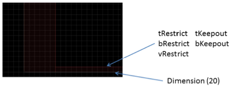
The diagram here shows the bottom-left corner of a PCB. The outline of the PCB is drawn in the Dimension layer with a width of zero.
For the Restrict/Keepout layers, five rectangles (all on top of each other effectively) were drawn for each side of the PCB. These five layers prevent components from being placed too close, it prevents vias and also tracks.
Note that the rectangles on the left edge of the board are quite wide. This is because this board was intended to be slid into a grooved metal enclosure along that edge. The metal groove was required to be kept totally away from components, vias and tracks.
In practice select the rectangle tool ![]() Then select the layer you want to perform the operation on
Then select the layer you want to perform the operation on
How to Define Mount Holes
About 10 minutes into the video Lesson 12 “Six Questions and Answers”
Select the hole icon ![]() Select the grid tool and select units you want to use to specify the hole size (mm or inches). Next select the hole size from the drop-down menu or if it is not there simply enter it in the Drill field.
Select the grid tool and select units you want to use to specify the hole size (mm or inches). Next select the hole size from the drop-down menu or if it is not there simply enter it in the Drill field. ![]()
How to Setup and Snap Parts to the Grid
2. Nudge all parts onto this grid. Hold down the CTL key as you select the part and its origin will snap to the displayed grid. You should not break this rule unless you have a very good reason. [1-3]
How to Quickly Simplify the Design by Removing Ground Air Wires
Source: https://learn.sparkfun.com/tutorials/designing-pcbs-advanced-smd/eagle-smd-pcb
The GND air wires can be distracting. Recommend initially removing using Method #1 and after parts are in place actually sending parts to ground using method 2.
Method #1
Right-Click a GND point and selected Property (or select the ![]() Info Icon) and then click on a GND wire. See the box at the bottom that says ‘Air wires Hidden’? Check that box and click ok. This will make all the ground air wires disappear! We’ll get the GND wires with a polygon pour later on.
Info Icon) and then click on a GND wire. See the box at the bottom that says ‘Air wires Hidden’? Check that box and click ok. This will make all the ground air wires disappear! We’ll get the GND wires with a polygon pour later on.
Method #2
This method solves the problem by sending all grounds down to the ground plane and remove redundant routes. See the “Ground Plane and Power” section for more guidelines.
- Make air wires visible if they are invisible (method #1)
- Using the Show Tool
 Click on a GND to easily see where all the grounds are
 - Create a via and place next to a GND pin. Name
 the via GND .
 - Using the Copy Tool
 , make copies of the vias and place next to all the GND pins
 - Rerun Air Wires by clicking the Ratsnest tool
 . Ground air wires should now be connected to GND vias.
 - Run traces from the ground pins to the ground vias

- Add a Ground Plane to the bottom of the board.
- Show ground plane by clicking the Ratsnest tool
 . Remove Ground plane by selecting the ripup tool
  and clicking on the ground plane line.
Design Part Placement
- If possible, keep 4 mm border around PCB clear of parts. This avoids interference with a reinforcing rib that runs around the bottom of the chassis. Conversely, if this is not always possible, gaps may be made to avoid parts.
- Surface-mount devices (SMD) are better than leaded devices in dealing with RF energy because of the reduced inductances and closer component placements available. The latter is possible due to the reduced physical dimensions of SMDs. This is critical to two-layer board design, where maximum effectiveness from noise-control components is needed. [ref 2 section 1.2]
- The term “Board Zoning” refers to the process of defining the general location of components on the blank PCB before drawing in any traces. Board zoning goes a little bit further in that it includes the process of placing like functions on a board in the same general area, as opposed to mixing them together. High-speed logic, including microcontrollers, are placed close to the power supply, with slower components located farther away, and analog components even farther still. For more on this topic read section 2.3 “Board Zoning” in “PCB Design Guidelines, For Reduced EMI” document [2]. For PaperBot this goes in the “Next Time” category.
- The topic of “Basic Loops” is beyond the scope of this document. The serious PCB designer will want to read TI’s excellent “PCB Design Guidelines, For Reduced EMI” document [2] and for this topic Section 1.4 “Basic Loops.”
Bypass Capacitors
The only non-dc current that should flow in the power routing of the PCB is the current required to replenish the bypassing capacitor. High-frequency current used inside the microcontroller that is switched on the input clock edges should come from the bypassing capacitors, not from the power supply. [2 section 2.1]
- Place capacitors that bypass bias supply voltages and reference pins (if any) of all ICs physically close to the corresponding pins. For driver chips use a combination of a large capacitor (10 µF – 100 µF) and a small ceramic capacitor (0.1 µF – 1.0 µF). [4-5]
Place filter capacitors so that their leads physically go right into the printed circuit board traces that carry mainstream of the current to be filtered. [4-6]
How to Move & Rotate Parts
CTRL + MOVE to snap a part’s origin in the current grid.
Type “rotate r45“, then click on the object you’d like to rotate by 45 deg counterclockwise. To rotate it clockwise type “rotate r-45”. Type “help rotate” to open the EAGLE help and read more about that function. What you type is not case sensitive.
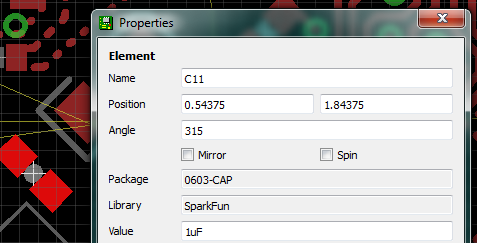
Another way to rotate a part is to select the part with the properties tool ![]() and typing in the desired rotation angle
and typing in the desired rotation angle
Type “SHOW Part Name” to find a part on the schematic.
Design Guidelines for Traces (Nets)
- Here is a list of general Design Guidelines that Sparkfun uses when creating the PCB layout. The SparkFun’s Better PCBs in Eagle tutorial provides this advice
Just because a fab house can handle down to 5mil traces and 6mil spacing doesn’t mean you should design with those sizes. If your board can be routed with 10mil traces and 10mil spaces, do it! The smaller you make things, the more likely you will get a PCB with broken trace (traces less than 10mil) or two traces touching each other (less than 10mil spacing between traces).
Even complex boards with tight pitch packages and a horrible rat’s nest of traces can be routed with 10mil traces and 8mil spacing. Next time you route a board, try it with 10mil traces and see just how far you can go – you’ll be surprised. If things get really tough, 8mil is usually ok. The goal of all these tricks and rules is the limit the spots where manufacturing failures could occur.
- Here is a CircuitCalculator.com you can use to calculate trace widths. It is interesting that a 10 mil trace width over a length of only 1 inch has a resistance of 50 mΩ – not acceptable for any non-signal trace. Unfortunately, a 16 mil trace is not that much better at 30 mΩ.
- For a general discussion on this topic read “Trace Width” in WikiBooks [3]
- Minimum drill size should be 15 mil. [1-10]
- Minimum annular ring size should be 7 mil. [1-11]
- 7 mil is the minimum size for traces. 8mil is acceptable. When possible try to keep the traces size to 10mil. [1-12]
- Use thicker traces for power lines. 12mil=100mA max, 16mil=500mA max etc. [1-13]
- 7mil between traces and space is reasonable. [1-14]
- To prevent pours from shorting to traces make sure you use a 10mil to 12mil isolation setting on any of the ground pour. [1-17]
How to Hand Route a Trace (Net)
- Lesson 12 “Six Questions and Answers”
- Using Eagle Board Layout
- Cadsoft EagleCad Tutorial Lesson 8
- Cadsoft EagleCAD Tutorial – Crucial Routing
Use the Routing and Ripup Route (not delete) tools ![]() to do manual trace runs.
to do manual trace runs.
The Cadsoft EagleCAD Tutorial – Crucial Routing starts with a surface mount board with battery, voltage regulator, and PIC processor. Ground Plane Border set in Tools – DRC – Distance & Copper/Dimension to 10 mm. Here is a video of a PIC board he may have built (or purchased from SparkFun) board like this in this video. Nice tutorial on the crucial wires on a microcontroller board and how to run them.
Manually Setting the Width of a Trace
If you do not see the trace width you want from the drop down menu you can enter it manually.
How to view a Trace.
The show tool ![]() mentioned in lesson 7 can be used to select a trace in the schematic window and then easily find it in the board window. As mentioned earlier, do not use the switch view button; instead click between windows.
mentioned in lesson 7 can be used to select a trace in the schematic window and then easily find it in the board window. As mentioned earlier, do not use the switch view button; instead click between windows.
Moving the Starting Point of an Air Wire
Eagle “air-wires” show the shortest distance between two points. Often the start and/or end of these air wires do not correspond to where you would like to start and/or end the trace. Solution: In the route mode Ctrl+click on a trace or pad picks starts an air wire.
Here are some alternative solutions to this problem.
Source: Strategic Digital Eagle Central Forum
Start the route from the opposite end of the air wire, which is often where you want it. Then manually route the wire along the path you like, finally connecting it to the existing routing.
After all of this, redo the ratsnest. If the additional wires you added get the job done, then the original air wires will go away. HOWEVER, if your grid prevented you from getting exactly to the correct point, then you’ll have a tiny air wire that you’ll have to route in a second try.
Sometimes if a route goes directly between three points (A,B,C) you are in a hurry so you run the trace from the point A to the point C, crossing over B. This leaves an air wire between the first and second point (Frustrating). Rip-up wire and do in two steps A to B, B to C.
Sometimes, you get these zero-length air wires that are difficult to find. Turn off all layers but air wires, and you’ll see them. Sometimes, you have to move one thing aside to give the air wire length, route it, then move the one thing back.
Vias
Drill Size
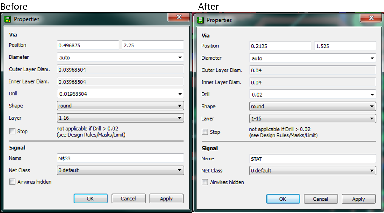
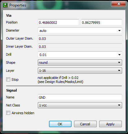
While Eagle likes it Drill sizes in metric, Sparkfun prefers English. Consequently, Eagle specifies a drill size of 0.5mm as 0.01968504 inches. For this instance Sparkfun requires the drill size to be 0.02 inches. Not sure who is correct, probably dependent on location of fabrication house. Follow these instructions if you want to conform to the Sparkfun standard. Specifically, if you follow these instructions, while you will pass the Sparkfun DRC, you will fail the Eagle DRC. Regardless of how you define vias (Eagle Default or Sparkfun), you will pass other DRCs (OSH Park, ITeadStudios, and 4PCB tested)
Original source:
http://www.eaglecentral.ca/forums/index.php?t=msg&th=37852&start=0&b786fff3c9d8e00cdcc028e5c873a84b/
For small round vias, in place of Default Drill ![]() Set to
Set to ![]()
If you have hundreds of errors, like I did you can type at the command line “change drill .02 in” or select change tool ![]() Drill and 0.02. Now just click on the small vias
Drill and 0.02. Now just click on the small vias
Here are the vias for the ProMicro. I can replicate properties in Eagle but DRC error results. Surprisingly this does not occur if you DRC check the ProMicro.
SparkFun
Update 7/13/2016
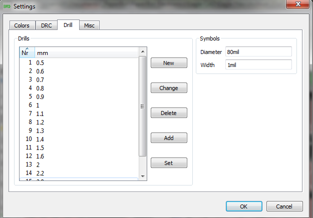
You can set the values that appear in the Drill size drop-down menu by going to Options – Set… – Misc, Open the Drill tab.
Routing Traces
To understand the theory behind routing traces read “PCB Design Guidelines, For Reduced EMI” document [2], Sections 2.4 “Signal Traces.”
- Avoid right angle traces – This advice comes from Pete at Sparkfun.
- Run traces perpendicular to each other (top and bottom layers) to reduce cross-talk and simplify the layout.
- Take a look at the design globally and decide if traces on the top layer should run horizontally or vertically. Take into consideration IC orientation, longest traces, and minimizing the number and length of traces on the ground plane (see Figure).
- For our design, traces on the top layer should run vertically
C POOR – Slot formed by 100-mil spacing cuts up ground plane and focuses slot antenna radiation into that connection
D BETTER – Ground plane extends between 100-mil centers
- Running traces in parallel even for a short distance on the same layer should be avoided to further reduce cross-talk. If unavoidable and traces are “noisy” consider surrounding with ground traces.
- Rule 1 can be changed “locally” to minimize vias and facilitate routing, but should be followed globally.
- To minimize vias, nudge/move and/or rotate capacitors and resistors to facilitate the route by using these parts as bridges, having traces run between them.
- Avoid sharp (90 degree) corners. Straight lines with 45 degree corners are preferable. Exceptions may be made to this rule as demonstrated on this sample PCB. [1-15]
- Assuming top-bottom traces run perpendicular to each other (Design Rule 1), to drop a via make a 45 degree turn drop via and make a second 45 degree turn.
Designing a Ground Plane and Power Distribution
Short Answer
Star distribution of power versus daisy chain (easily forgotten) and a Ground Plane
Two-Layer vs Four-Layer Boards
A two-layer board can achieve 95% of the effectiveness of a four-layer board by emulating what makes a four-layer board better. [2 section 2.1.2]
- Make an extra effort to route ground underneath power, which reduces impedance and minimizes loop area. [2 section 2.1.1]
- Under the microcomputer, build a solid plane for ground that bypassing components and the oscillator loop can be tied to. Tie this ground to the ground pin and the power-supply bypass capacitor. This is called a microcomputer ground. [2 section 2.1.3].
Power Distribution for Two-Layer Boards
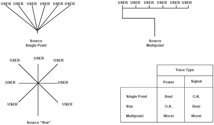
In a true single-point power-distribution system, each active component has its own separate power and ground, and these traces would remain separate until they meet at a single reference point. In multipoint systems, the connections are made in a daisy-chain fashion, so there are multiple 0-V reference points. It is clear that multipoint systems have the potential for common impedance coupling. While implementing a single-point system may be impossible, a combination of single point for devices generating RF and multipoint for everything else serves to reduce noise. The best scheme possible has a single point that ties together the regulator ground, microcomputer ground, battery negative, and chassis or shield (see Figure below). [2 section 2.2.1 Single-Point vs Multipoint Distribution]
How to put into practice a “Star Distribution” and “Gridding to Create Planes” are interesting reads in TI’s excellent “PCB Design Guidelines, For Reduced EMI” document [2], Sections 2.2.2 and Section 2.2.3. However, probably beyond the scope and time we have on the PaperBot project.
Using Autorouters with Ground Planes and Power
Autorouters for PCBs do not take any noise reduction actions; therefore, care should be taken in their use. Power and ground routing, as well as signals that impact susceptibility, should be laid out by hand. Any signal with clocked data, such as low address bits in a memory expansion bus, should be next. Only signals with switching rates below 50 kHz can be left safely to the autorouter. [2 section 2.6.3]
How to Make a Ground Plane and Copper Pours
Sparkfun https://learn.sparkfun.com/tutorials/using-eagle-board-layout
Nicholas Tip: Add a ground pour on both sides of your board.
Sparkfun Tip: Add ground pours to your design at the very beginning (after placing parts, before routing) makes manual routing much easier or simply bring up the property window on GND and turn air wires off.
To view the ground plane hit ratsnest. To hide the polygon (it’s hard to see other stuff with it on there), use the RIPUP tool on the polygon border you just drew. Don’t worry; the polygon is still there, just hit ratsnest to bring it back.
How to Make a Ground Plane
Set grid to 7 mil (NOT mm) grid ![]() before autoroute
before autoroute ![]() Then in set Routing Grid to 7 mil in the Autorouter Setup.
Then in set Routing Grid to 7 mil in the Autorouter Setup.
To add a ground plane (end of Lesson 9) select the Polygon tool ![]() , select the layer
, select the layer ![]() , top menu icons
, top menu icons ![]() and fields
and fields ![]() . To select the board, click the top-left, bottom right, and top-left (again) corner of the board. Zoom in as you hit each corner to make sure you get the right point, especially the closing point (top-left). Click the rats nest icon
. To select the board, click the top-left, bottom right, and top-left (again) corner of the board. Zoom in as you hit each corner to make sure you get the right point, especially the closing point (top-left). Click the rats nest icon ![]() to add the ground plane. Each time you open the board the dotted lines will be shown. To see ground plane again click on the rats nest icon.
to add the ground plane. Each time you open the board the dotted lines will be shown. To see ground plane again click on the rats nest icon.
Excerpt from Crucial Routing at 10 minutes into the video. To modify the ground plane, in this case to move it closer to the edge of the board, select the unroute tool ![]() and click twice on the line defining the ground plane. The ground plane is removed, yet the outline is kept in place. Right clicking the wire moves you to the other side of the board (toggle between top and bottom ground planes). Go to Tools
and click twice on the line defining the ground plane. The ground plane is removed, yet the outline is kept in place. Right clicking the wire moves you to the other side of the board (toggle between top and bottom ground planes). Go to Tools ![]() and DRC. Click on the Distance Tab. Change
and DRC. Click on the Distance Tab. Change ![]() to 10 mil. Hit return (Apply does not close the window) and again add the ground plane by clicking on rats nest icon
to 10 mil. Hit return (Apply does not close the window) and again add the ground plane by clicking on rats nest icon ![]() . Now it goes right to the edge. I put the Copper/Dimension back to its default value when I was done.
. Now it goes right to the edge. I put the Copper/Dimension back to its default value when I was done.
How to Make Copper Pours
HOW-TO: Polygons and ground fills for PCBs in Eagle ß Required Reading
Covered in the reading is the concept of rank.
One of the problems with Eagle CAD is that it cannot end a trace without rounding the end. This is normally a problem when you want to add large power traces. This tutorial shows you how to solve this problem and consequently add a power pour.
- First, define polygon
 with a 0.001 width. Minimum width shown will be 0 and 0.01. Pour will be along outside border of the trace. If you use zero you will get a lot of DRC check errors and CAM processor will fail (actually take forever after warning you). At 0.01 the CAM processor will complete nicely, you still get all though DRC errors. The minimum trace size allowed by OshPark is 6mils so you can try that – but DRC seems to complain below 8mils.
 - Name using naming tool

- Use delete not rip-up to remove
- Left-click and select properties – for top layer power pour turn thermal off.
“With thermals on, a pin will connect to the polygon through small traces extending from the pin center in 4 directions. Thermals make soldering easier, the part heats faster because the heat is not dissipated as quickly.
Disable thermals will make a solid pour trough the pin/pad. We usually use thermals. We only turn it off on high power traces that require more conductivity between the pad and the polygon.”
- You may also want to set properties as described in the article. Units in article are in mm.
- To temporary remove or hide the copper pour, select the RIPUP tool and click on the polygon. It removes the copper pour while keeping the polygon (dotted lines). Click RATSNETS again to recalculate the copper pour.
- Verify that pour isolation is 0.012, if not follow instructions in Better PCBs in Eagle
How to Define Multiple Ground Planes (not recommended)
For some applications, you may want multiple grounds, as is done with charger booster. Add two different ground symbols (GND, GND1). You can find them by searching for supply*. Next answer no when asked to merge traces. From now on you will get an error from Eagle which you may ignore.
Silk Screen Layer
Rules 4 – 8 in reference document 1.
- Devices should be labeled with their purpose [4-4 to 4-7]
- LED (power, status, D4, Lock, etc).
- Connectors: e.g Vin, Port1, Batt, 5V, etc.
- TX, Power, +, -, Charge, etc.
- Switches and switch states: eg. On, Off, USB etc.
- Add off-white bounding rectangles with labels to separate a complex design into various smaller modules (for example, LiPo Charger, Boost DC-DC Converter, etc).
- When applicable, it is better to avoid having vias go through the silkscreen when adding labels. [4-8]
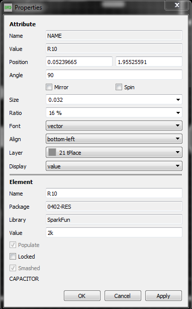
How to add origins to Part Names
If we want the names of components to be legible on the top of the board (transferred via toner transfer), or just to look good on printouts, then names and values probably have to be moved from their default locations. In order to move the text separately from the device itself, we use the “SMASH” command. Turn your EAGLE schematic into a PCB
Set origin point (bottom-left, top-right …) in property menu.
Make sure vector is set.
Autorouters
Other than help guide the placement of parts I do not recommend Autorouters
Before you auto-route all power/ground signals should be routed. Reserve autorouter for signals.
Before You Start Set Defaults
- Grid – finest (button on the right of size and alt text entry boxes
- Vias to finest 0.02
- Trace width to finest 0.008
Do a final design rule check.
Save with name ROUTE
Choosing a PCB Fabrication House
PCB Manufactures
Summary
After reading the following material it appears you send your board layout to Advanced Circuits (4pcb) if you want high quality, fast turn-around, at a fair (not low) price. Lowest price is with their barebonespcb.com company. Batch processing companies while taking longer (weeks versus days) still provide high quality boards and at a much lower price. The names that keep appearing here are OSH Park, ITeadStudio, and SeeedStudio.
Research
PCB Price Comparison: Compares prices from 25 PCB manufacturers at once
For traditional manufacturing consensus seems to be Advanced Circuits (4pcb.com) aka Barebones PCB aka 33Each.com aka FreeDFM.com. Read about pricing and alternative companies from this Lady Adafruit article. Quoting article…
The fastest is barebonespcb.com , which will get your boards shipped next day, no solder mask, etc. for $35 and a sq. in. cost. This seems to be one of the cheaper method available online. I’ve used it a lot and have no complaints. Since it’s square-inch priced you can panelize (put mulitple designs on one PCB and cut it with a saw your shear)
Another method, if you’re a student, is their $33 deal where you can get a 60sq.in. board for $33 ($50 after shipping) with soldermask and top silkscreen. If you’re not a student, theres a 3-part minimum, so its $100. Still, a good deal if you want soldermask. If you want to panelize this design they’ll add $50.
They’ll rip you off on shipping, so be sure to calculate that into your total!
In addition to PCB Manufacturers, you may want to consider “Batch” manufacturing services. These services will make nice PCBs in small quantities but they can take weeks – they basically collect a dozen orders and tile them into one PCB which is why there’s a delay.
Lady Adafruit: OSH Park, ITeadStudio, SeeedStudio Fusion
Sparkfun Recommends: OSH Park
Cheap PCB Manufacturers: Seeed Studios, OSH Park, Olimex, ITeadStduio, PCB Cart
Notes:
- BatchPCB was a part of SparkFun and used Gold Phoenix for downstream provider.
- BatchPCB has been purchased by OSH Park. Domestic downstream provider.
UFO Ab-ducted (by Tien) located Bay Area Circuits cost was $30.00 + $12.00 for 2 (sent 6) from order to delivery 8 days.
PCB Board Specifications (PCB Quality)
Sparkfun
- SparkFun uses 1 ounce copper on boards (versus 2 ounce copper board)
OSH Park
- All 2 boards are FR4 170Tg/290Td which is suitable for lead-free processes and temperature.
- They have ENIG (gold) finish for superior solderability and environmental resistance.
- They’re6mm thick (0.063 inches) with 1 ounce copper on both sides.
- The minimum specs for 2 layer orders are 6 mil traces with 6 mil spacing, and 13 mil drills with 7 mil annular rings.
- Internal cutouts are allowed and supported. Draw them on your board outline layer.
- Plated slots are not supported.
ITeadStudio (i.e., iMall)
Normal Condition of PCB capabilities
They’re 1.6mm thick (0.063 inches) with 1 ounce copper on both sides.
Basic Surface Finish is HASL. Lead Free HASL is an additional $10.00. ENIG (gold) finish is an additional $20.00. I Upgraded to ENIG without a cost penalty! Advantages of HASL are excellent wetting during component soldering and finish avoids copper corrosion. Disadvantage of HASL is low planarity on vertical levelers which may make this surface finish unsuitable for use with fine pitch components. High thermal stress during process may introduce defects into PCB.
Bay Area Circuits
California based, fast turnaround at a low price for students.
Bay Area provides its own PCB layout tool named PCB Creator. For Eagle send them Gerber Files as .ZIP in RS-274x Format with Board Outline and NC Drill File Included.
Engineering Tools (Array Calculator, DFM Report, DXF to Gerber Conversion, Glossary of Terms, Panelizer Tool, and PCB Design Tool.
Design Rule Check (DRC)
As you proceed in the design of your board, do a design rule check DRC often against the PCB house that will be fabricating your board. Before you do the DRC enable all layer. Hidden layers are not checked, like exclusion zones!
Each PCB fabrication house has its own set of Design Rules. They typically provide these as DRU files for Eagle. I recommend checking your design against as many DRU files as possible, including the Eagle Default. If you are in a hurry, I have made two composite DRUs (3DoT-2-layer-STANDARD and 3DoT-2-layer-TIGHT) located in the 3DoT_DRU Folder. These DRUs were derived from SparkFun, iMall, 4PCB, and OshPark.
Before you begin…
- Download a DRU file and place in the Eagle DRC folder.
- Select a DRU file by clicking on the DRC icon –
 , press the Load… button and then select a PCB_Company.dru.
 - While most DRU files verify that all angles are multiples of 45 degrees, some like OshPark do not. Verify that your selected DRU file includes this test by clicking on the “Misc” tab and verifying that the “Check angle” box is checked.
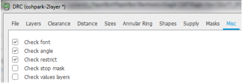
- If you need to check this box, make sure you save the new DRC configuration.
Whenever you run a DRC…
- Enable all layer. Hidden layers are not checked, like exclusion zones!
- Fill your polygons with copper (also known as a copper pour), by clicking the ‘Ratsnest’
 icon . Why clicking the Ratnest icon would perform a copper pour is one of those inexplicable Eagle CAD mysteries. Without this step unrouted ‘airwires’ may go undetected.
 - Verify DRC is checking angles (see Step 3 under “Before you begin…”)
The TQFP version of PaperBot has passed Oshpark, iteadstudio, and Sparkfun DRCs. It fails the Eagle default DRC which appears to be the hardest. It is interesting that the original design was created against the Sparkfun DRC, which I believed was the most rigors. After passing the DRC, it failed on other DRC checks in other areas.
Material from My Sources
Sparkfun
We are constantly pushing ourselves for better printed circuit boards (PCB). One thing we’ve learned is that PCB fab houses (such as Advanced Circuits, BatchPCB, PCB123, Gold Phoenix, Bare Bones PCB, anyone really) have a very hard job to do. Creating a PCB is not an easy task and there are many ways for a fab house to mess it up. Unfortunately, fab houses tend to spend less time on prototypes than on production runs. Therefore, we try to design products and PCBs for ‘manufacturability’. This tutorial will show you how to minimize the number of ways the fab house can screw up a PCB and includes a link to Sparkfun’s DRC.
Before they fabricate the board, the fab house will usually run a quick “design for manufacturability” (DFM) check, and let you know if something on your design will cause in a problem. Source: https://learn.sparkfun.com/tutorials/using-eagle-board-layout
OSH Park
You can download our Eagle DRU file which will verify that your design meets our design rules:
- 6 mil minimum trace width
- 6 mil minimum spacing
- At least 15 mil clearances from traces to the edge of the board
- 13 mil minimum drill size
- 7 mil minimum annular ring
File named LaenPCBOrder.dru, have renamed OSHPark.dru and made changes as discussed in “How to Tent Vias” section below.
Here are the step-by-step instructions for generating the CAM files
- Generating Custom Gerbers from Eagle
- For earlier Eagle versions file is named OSHPark-2layer.cam
- For Eagle 7.2 and above file named OSHPark-2layer-Eagle7.2.cam
Warning: OshPark DRU does not tent vias
ITeadStudio (i.e., iMall)
How to Export Gerber files from Eagle
https://www.itead.cc/blog/how-to-export-gerber-files-from-eagle
Be patient may take a while for article to load.
I found DRU and CAM files here
http://store.iteadstudio.com/index.php?main_page=product_info&products_id=175
Historically, I have found and downloaded DRU and CAM – see older Eagle folders (cam and dru folders) for what I have.
4PCB
This article takes you through the final design checklist and step by step instructions for getting your design to 4PCB.
CAM (Gerber) Files
Getting Everything Ready
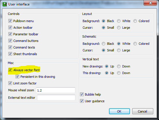
Set output Fonts as Vectors
By default, vector font aren’t enabled, and not using them can make a mess of your Gerber files when it’s time to go to production, so go to your ‘Options > User Interface…‘ menu item, and enable the checkbox below if it isn’t already. Your board manufacturer will thank you for it. Essential Eagle Skills: Use Vector Fonts!
Tent Vias – Defining
Sources:
- Better PCBs in Eagle section”Tenting”
- FCS Eagle – Frequently Asked Questions (FAQ) Question #13
Here are instructions for tenting vias from OshPark. http://docs.oshpark.com/design-tools/eagle/design-rules-files/
Running DRCs will remove tents unless programmed otherwise.
| March 7, 2016 Addendum, Updated July 6, 2016 – Nicholas Lombardo Trick |
Tenting is taken care of in Eagle by modifying the DRC rules. To see if the vias will be tented or not, turn on all the tStop and bStop layers.
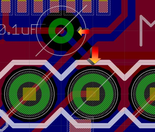
Turning on all the layers will create a lot of noise in the display of the board. What you are looking for is the white hatch marks indicating where the will be a lack of solder mask. The upper arrow points to a via that has no hatch marks, indicating there will be no lack of soldermask on that via (tenting it). The lower arrow points to a large hole with a white hatch mark on top of it. This is a solder point that needs to be exposed. The white hatch marks indicate there will be a lack of solder mask over this hole, exposing it so that we can solder to it.
- Determine the size of the largest via
- Run appropriate DRC, but before you process, go to the “mask” tab and change the “limit” to be larger than the largest via. In mils (1,000th of an inch). Addendum largest via is 23.62 mils (0.023622 in). I set to 100mil. Sparkfun warns that if this number is too high you will cover important holes, like those meant to solder on connectors. The DRC setting is set to 25mil in the SparkFun DRC
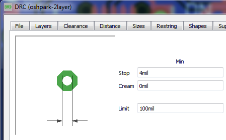
- Process DRC and then CAM as usual.
Alternatively, you can modify the dru file.
Tenting Vias – Verification
Author: Terri Miller
EAGLE generates by default a solder stop mask for each via (also for Pads and SMDs, of course). This means the via is free of coating material. The solder stop mask is drawn automatically in the layers 29, tStop, for the top side and 30, bStop, for the bottom side. The size of the solder stop mask can be determined in the Design Rule’s Mask settings. See the values for Stop. By default the value is fixed to 4 mils. Minimum and maximum are set to the same values therefore. If you want to have a diameter-dependent mask you could also define a certain percentage. The resulting value can be limited by a minimum and a maximum.
In order to have vias coated, EAGLE allows you to set the solder stop Limit in the Design Rules’ Mask tab. Here you can define a value which is dependent on the drill diameter of the via. Let’s assume you would like to set the Limit to 0.012 inch. Now all vias in the layout up to a drill diameter of 0.012 inch will be covered with coating material. All those vias that have bigger drills will stay uncovered. In case you want to have some smaller drilled vias uncovered, you have the possibility to select vias out of those that are covered in order to uncover them. This can be done with the command CHANGE STOP ON | OFF in the Layout
Blog Editor. This also works for groups.
You can quickly see if vias are tented by only tuning on layers 29 tStop and 30 bStop.
Creating Stop Mask
By the way: It is allowed to draw areas that should remain free of coating material in the tStop/bStop layers directly. But it is not possible to delete certain automatically generated solder stop symbols there. You have to deal with Limit and CHANGE STOP ON | OFF instead.
Verify pour isolation
Verify pour isolation is increased from 0 to 0.012 as discussed in Better PCBs in Eagle tutorial.
Define Silk Screen Layers
Before you begin you will want to take a quick look at the layers you want to use for the top and bottom silk screen layers. By default these are tPlace, tName, Dimension and bPlace, bName. Other layers you may want to include may be your logo or tValues. Once you are happy with the silk screen layers to be used, name the layer images topsilk and bottomsilk. To do this, right-click layer icon ![]() and select New…
and select New…
Now you can open it quickly anytime you want. You may want to verify no other layers have, been included by accident by opining the edit window for each layer description. Right-click layer icon – Right-click definition (ex. topsilk).
Build Folders
Make sure PCB has passed both iteadstudio and OSHPark design rule check. Make two new folders with postfix _OSHPark and _iteadstudios. Place copies of schematic and board files in each folder. I go through process first with OSH Park which provides a visual of how the final board will look, an excellent feature not provided by iteadstudios. Here you can check artwork and verify vias are tented.
Basic CAM Process
Update Sunday, January 08, 2017
Current 3DoT Gerber files are generated by following SparkFun’s directions:
https://learn.sparkfun.com/tutorials/using-eagle-board-layout/generating-gerbers
Update Thursday, May 26, 2016
When you run a CAM job you may get a warning that process may take a very long time. Go ahead and try. If it really does take forever. Look for custom pours with 0 line width as discussed here.
Sparkfun
Update Thursday, May 26, 2016
Downloaded SparFun_Eagle_Settings files from Github.
The original tutorial link is from November 06, 2008, here is another named Using EAGLE: Board Layout that is unfortunately not dated.
Original
Although they do not fabricate PCB[1] they still provide a helping hand.
- Better PCBs in Eagle Section Gerber File Generation
Please start with our CAM file – and modify if you really need to. We’ve used this CAM file thousands of times without problems.
We’ve changed the default Eagle CAM file so that it does not mirror any of the bottom layers (number one problem with gerber submissions!), it outputs a standard Excellon drill file (second most common error is a missing drill file), and captures only the tPlace layer onto the silkscreen layer (this will cause all part identifiers and values to not print on the silkscreen). Put all text and labels onto the tPlace layer that you want to see printed on the board.
[1] Actually they used too but sold BatchPCB to OSH Park.
OSH Park
Download and add the OSHPark-2layer-Eagle7.2.cam to the Eagle 7.3.0 CAM folder.
Here are the step-by-step instructions for generating the CAM files for OshPark Generating Custom Gerbers from Eagle . They are summarized here and updated to Eagles new User Interface (UI). If you are in a hurry you can skip steps 1 to 5 and simply upload the Eagle Board file… but that is way to easy!
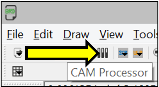
- Open the CAM Processor

- Open the CAM job
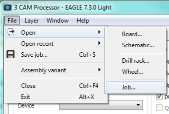
- Each tab across the top of the window corresponds to one of the files (“gerber files”) used in manufacturing your board. “Top Layer” defines what gets etched into the copper. ”Top Soldermask” defines what gets exposed through the soldermask. ”Top Silkscreen”– you guessed it– defines what is printed on your board.
- Run the CAM job to generate gerbers. Click the “Process Job” button. This will generate a bunch of files ending in “.ger” and one ending in “.xln”
- Zip them up and upload to com
- I often get red warnings about my email address.
 Just click warnings after you have entered your email address and they will go away and the continue button will light up (poor user interface).
 - The beauty of OshPark now appears as you gaze on what your completed board will look like. Take a very close look and make sure it is what you want. Are parts all named, are vias tented, etc.
ITeadStudios
- You can skip this article, DRU and CAM files up to 6.X located in response to first comment. Here is another useful comment. Addendum: From the comment on reference blog post.
| CJ van der Hoeven on July 25, 2015 at 12:22 pm said:
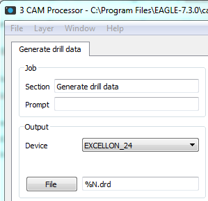
Recently I have upgraded to Eagle 7.3. As a result, I get wrong coordinates in the excellon drill file when examining the drill file with gerberviewer. Further investigation shows that Eagle (CAD-Soft) has changed the resolutions of all coordinates in the drill file. So the original format is still available as an option. So drill files should be generated with option “EXCELLON_24″ instead of “EXCELLON”. This is applicable to Eagle version 7.2 and 7.3. Could you please confirm and add this info on your web page for other users? |
Repeat OSH Park Steps 1 to 4 with Iteadstudio_CAM6 file. Modify Step 2 to select EXCELLON_24 device from the drop down menu. Run and Save project when you are done.
- Once completed, I was able to upload to OSH Park in order to view PCB. Note: vias were not tented and am not sure how to force this issue. You can also use a 3rd party “gerber viewer” to see what your completed PCB will look like. This online viewer is pretty basic but it does work. To use, “Choose File” then turn on (check mark) all the gerber files shown on the right. Otherwise it is just a blank screen (poor user interface).
- ITead Studios charges in increments of fixed board sizes. PaperBot Board size = 3.5cm x 6.9cm so you would order a board with a maximum size of 5cm x 10cm
- Unlike OSH Park you must pay for the board before you upload the zipped Gerber files – a system headed for frustration versus OSH Park which will not charge you until they understand what you want.
4PCB
This article takes you through the step by step instructions for getting your design to 4PCB.
Stencil for Solder Paste
Now that the board is finished and ready for fabrication, the next step is to get the Surface Mount Devices (SMD) squared away for soldering. This entails designing a stencil that masks out the entire board except for the pads of the SMDs. This is one of the easier parts of the PCB fabrication, it involves viewing and changing one layers setting of the board.
Following are three approaches that first two show how to have the stencil professionally made and the second steps you through making a stencil by hand.
Generating Solder Paste Stencil and Ordering through OSH Stencils
Like OshPark for Stencils. Go to OSH Stencils click Upload Design. Follow step-by-step instructions. 3DoT PCB version 4.43 cost $8.27 with shipping. The PCB ordered from OSH Park cost $19.35 giving us a grand total of $27.62 for 3 boards and stencil. OSH Stencil also allows you to purchase a Jig for $5.00 more. Not considered important for this low run version.
These are lower quality stencils good for maybe 30 plus boards. The next options gets you stainless steel stencil.
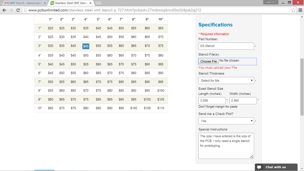
Generating Solder Paste Stencil and Ordering through PCB Unlimited
Stencil File
We will generate a Gerber file for the SMD components solder paste areas using the Eagle PCB .brd File.
First, click the CAM Processor button:
Click File>Open>Job and navigate to the desired CAM file. This tutorial uses SparkFun’s CAM File.
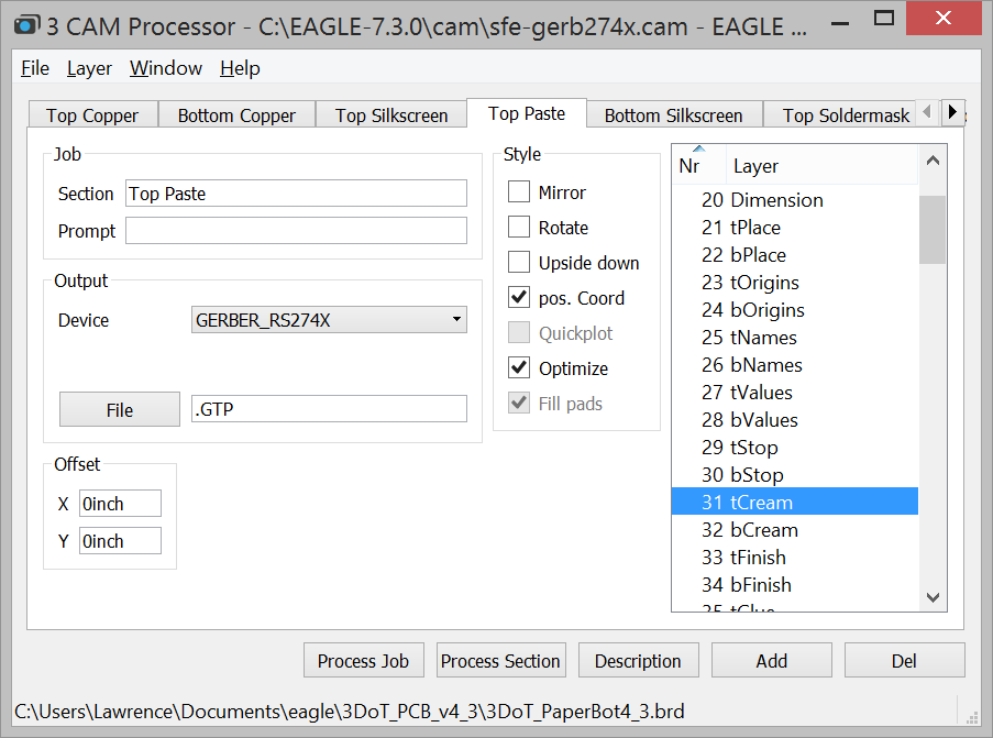
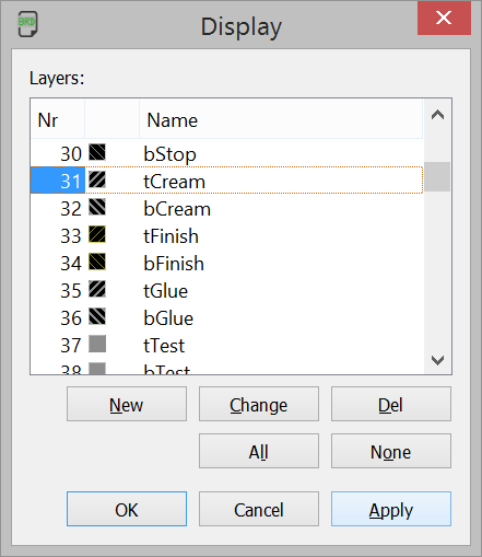
To generate a Gerber file for the solder paste areas use Layer 31 tCream. Using the SparkFun CAM File, you can select the Top Paste tab. Click Process Section to generate the Gerber file for this layer only (Process Job will generate the various Gerber Files defined in the CAM File). The resulting file will have the extension .GTP (Gerber Top Paste).
PCB fabrications houses use Gerber files so they do not have to support files from various PCB CAD programs (Eagle, OrCAD, DipTrace, etc.).
SMT Stencil: http://www.pcbunlimited.com/
Make sure to select Yes for “Send me a Check Plot” to verify the stencil before it is produced. 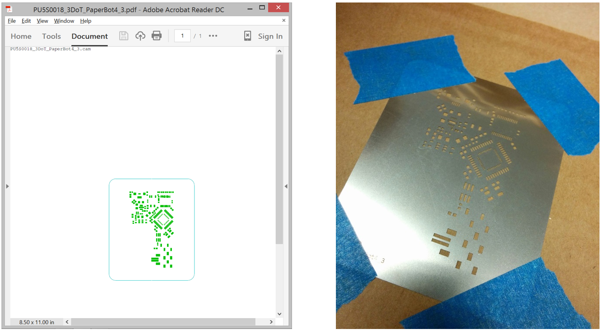
-Check plot in pdf format received 2 business days after order was placed
-Shipped in 3 business days, received in 7 business days
Make Your Own Stencil
This section follows the steps defined in this Instructables for making a stencil from a soda can. http://www.instructables.com/id/Easy-Aluminum-Solder-Mask/
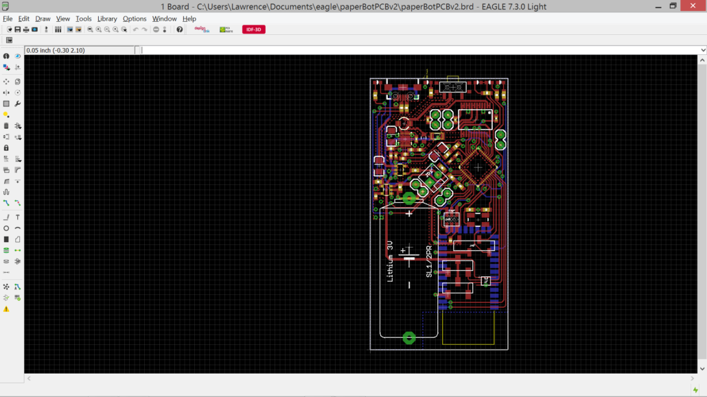
For example, let us use a rather involved/dense board:
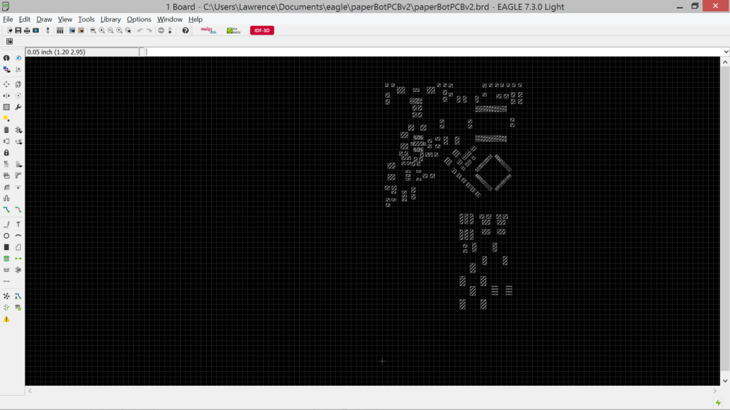
- Click the layer settings icon . Next, turn off all layers by clicking “None,” and turn on layer 31 “tCream,” only. Hit apply.
The example board is as follows:
- Only the pads requiring solder paste will be visible with diagonal hatch marks. To create the stencil, these hatch marks need to be turned off. This is done by changing the layers view options in layer settings
 . Double click layer 31 “tCream” and change the fill style to the solid black box by clicking:
This fills the middle of the “tCream” layers elements with the specified background color, which is black in the default case. This results in grey outlines of the pads for the SMDs: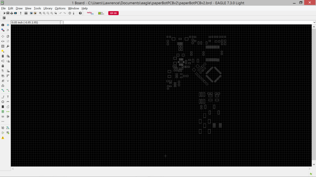
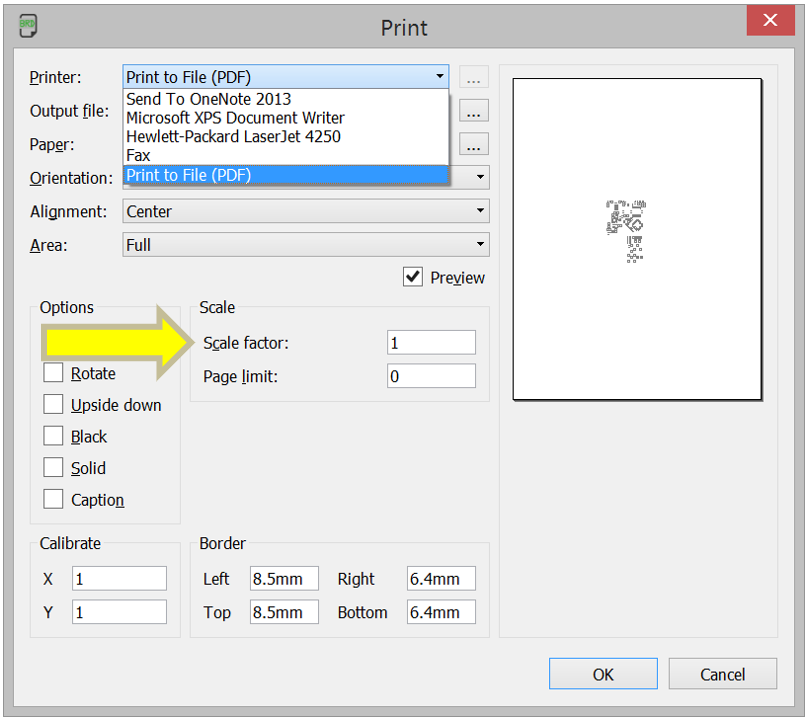
- Next go to File>Print, or Ctrl+P. For “Printer” select “Print to File (PDF)” and make sure “Scale Factor:” is set to “1”:
Expert Tip: Pay Attention to “Output File” so the resulting PDF can be found and used for subsequent steps.
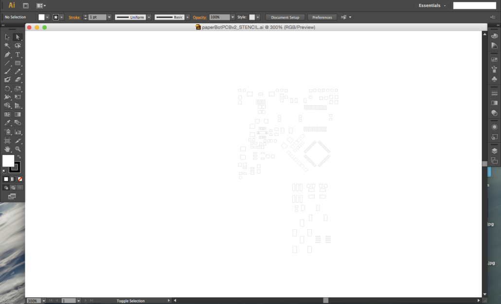
- Open the PDF file created in the last step. In the center of the page should be an outline of the SMD pads for the board. Now, any number of graphic design/vector art/illustration software programs can be used to duplicate or manipulate the stencil and dimensions. Adobe Illustrator is shown here:
Bill Of Material
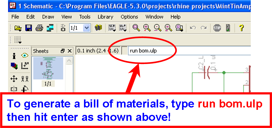
To create a Bill of Material (BOM) type run bom.ulp script. Verify all parts are in sequential order (ex. C1 to C17). Save as Text. Import into Excel.
Appendix
SimpleBot Design Example
- PaperBot 4.46a OSH PCB, a fabrication ready board.
- SimpleBot DEMO
- Run ERC
- Put micro-USB connector back or switch to a 328P w/ program header
- Power connector – switch to 9v standard conical connector
- Finding the right part. Try the normal way (barrel jack, jack …). Alternative, go to open source community like Arduino and Sparkfun, find board with part and copy – paste. Copy tool, Group tool, right-click copy group, select paste tool (yellow ball).
- Ground and Power distribution, Ground pour on both sides, star power
- Grid, default English units, divide by 2 as needed, Display ON
- Look over the landscape – delete randomness pieces laying around
- Ground and Power distribution, Ground pour on both sides, star power
- Select all and rip-up to return to air wires. Warning: air wires simply connect to the nearest point and may not reflect the best point to connect to or best route.
- Part Placement, Crystal as close to MCU as possible. IC bypass capacitors (as close as possible, power to pin, ground to pour), LEDs to edge of board, Power filter/bypass capacitors next to power source.
- Find parts using show tool in schematic and visa-versa
- Lawrence tip: stretch parts out and uncross air wires as much as possible. Rotate as needed.
- Rotate, select rotate enter 45 in Angle: drop down box.
- Trace width (in this example all are the same)
- Ground over antenna, top and bottom
- Sequence part designators (names) to simplify BOM
- Snap parts to grid (ctrl-click)
- HC-06 to top of board (verify pins are correct)
- Custom CONN_HEADER_TOP 2MM pad dimensional error.
- Selecting overlaid traces (right – click)
- Layers – who is important and who can you forget.
- Values – not printed
- tPlace and bPlace – printed
- Custom layer views and how to define (left click layer settings)
- Ground Pours on/off (on ratsnest, ripup – off left border – right to layer – left click)
- Polygon pours (polygon tool, 2 widths, name w/o thermals)
- DRCs (recheck for air wires)
- OshPark Does not allow labels over vias. Always look for air wires after DRC
- Sparkfun Drill size, Angles
- 4PCB Possibly the most demanding (distance between traces etc.)
- Before ordering (see document)
- Vector letters
- Tenting Vias (see section on this topic)
PaperBot Design Specific
- I found an I2C female connector as an SMD device. Link in BOM and duplicated here:
http://www.digikey.com/product-detail/en/NPTC041KFXC-RC/S5596-ND/776054
- See if you can find part in Eagle library (I will also look around) and replace current 4-pin through-hole header.
- The I2C connector supports the Sparkfun module https://www.sparkfun.com/products/10724 which includes an accelerometer, gyro, and magnetometer.
- I cannot find a JST connector to replace current right hand version providing a plug-in option for an external battery or power supply. I will be replacing with a SMD version shortly. This connector is also placing a ground (and power) line over the Bluetooth antenna which is prohibited, so will need to relocate.
- With most connectors now placed over the Bluetooth module, we are forced to switch to surface mount versions. As TI points out this is also the best option from an RF perspective. Therefore, we need to find SMD devices for these other connectors (I will also be working on this). If we can’t find them it will be back to making custom parts.
- Add level converters for servos.
- Finally, I would like to add test points as the layout allows. The idea here is to finish the layout then look for areas that we can use as test points and add a 1 or 2 pin header at these points.
Deprecated
BSC
BSC means “Basic Spacing between Centers”. This is often used if the reference lines don’t refer to a physical point or edge, like in the case of the pins: the reference is in the middle of the pin, instead of one of the edges.
Gerber Files
How to create a Gerber File. First save everything ![]() (or it will not create the Gerber files). Click the rats nest icon
(or it will not create the Gerber files). Click the rats nest icon ![]() to see the ground plane. Open layers window
to see the ground plane. Open layers window ![]() and select All. Click on the CAM processor icon
and select All. Click on the CAM processor icon ![]() to open the CAM Job window.
to open the CAM Job window. 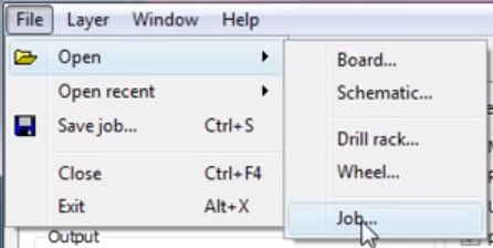
Click on the Execute Script icon ![]() and then…
and then…
Select  (downloaded earlier in lesson 10). SFE stands for Spark Fun Electronics. When you submit the job, the PCB house will ask you to upload each of the Gerber files created.
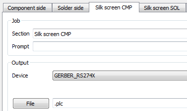
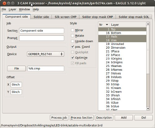
Knowing which one they want can be confusing (voice of experience), so click on the tabs to learn about what files are related to what information and see the associated extension. In this example, Silk screen CMP has the extension .plc.
Keep everything at default values, including name (or lack thereoff) and click on ![]() . If you get a save pop-up window say yes and then repeat process – after saving it does not create Gerber files. Open Control Panel to verify gerber files have been created.
. If you get a save pop-up window say yes and then repeat process – after saving it does not create Gerber files. Open Control Panel to verify gerber files have been created.
Silk Screen Layer
Moving to Lesson 10. How to add a Silk Screen layer. Download silk_gen.ulp and sfe-special.cam files from here http://rpc-electronics.com/eagle.htm. Place these files in their respective folder in Eagle (sfe and cam).
Click on the ExRun ULP icon ![]() and select. Say OK to Error message. Keep defaults and click on
and select. Say OK to Error message. Keep defaults and click on ![]() . Just say run on next window and you have your silk screen layer. In the layers window
. Just say run on next window and you have your silk screen layer. In the layers window ![]() you will now see our two new silk screen layers
you will now see our two new silk screen layers ![]() . Verify silk screen does not overlap any pads. You can move
. Verify silk screen does not overlap any pads. You can move ![]() or delete
or delete ![]() silk screen text by double-clicking on target cross
silk screen text by double-clicking on target cross ![]() . If you are moving, rotate by right-clicking.
. If you are moving, rotate by right-clicking.
Lesson 11. To add text to the silk screen layer, for example board name, author, date and/or version, click the text icon ![]() , type information, and then set properties. Author recommends Font as vector.
, type information, and then set properties. Author recommends Font as vector.
Vias and Solder Stop Mask – How Does it Work?
- Also known as Tented Vias
- Sparkfun uses tented vias where Eagle default is to add a solder mask.
- Sparkfun https://www.sparkfun.com/tutorials/115 see Tenting
EAGLE generates by default a solder stop mask for each Via (also for Pads and SMDs, of course). This means the Via is free of coating material. The solder stop mask is drawn automatically in the layers 29, tStop, for the top side and 30, bStop, for the bottom side. The size of the solder stop mask can be determined in the Design Rule’s Mask settings. See the values for Stop. By default the value is fixed to 4 mils. Minimum and Maximum are set to the same values therefore. If you want to have a diameter-dependent mask you could also define a certain percentage. The resulting value can be limited by a minimum and a maximum.
In order to have vias coated, EAGLE allows you to set the solder stop Limit in the Design Rules’ Masktab. Here you can define a value which is dependent on the drill diameter of the via. Let’s assume you would like to set the Limit to 0.012 inch. Now all vias in the layout up to a drill diameter of 0.012 inch will be covered with coating material. All those vias that have bigger drills will stay uncovered. In case you want to have some smaller drilled vias uncovered, you have the possibility to select vias out of those that are covered in order to uncover them. This can be done with the command CHANGE STOP ON | OFF in the Layout Editor. This also works for groups.
By the way: It is allowed to draw areas that should remain free of coating material in the tStop/bStop layers directly. But it is not possible to delete certain automatically generated solder stop symbols there. You have to deal with Limit and CHANGE STOP ON | OFF instead.
Create iteadstudio CAM file
You can find these initial steps defined here. As of this writing the comments with responses in this blog post had not been updated to Eagle 7.3.0 so these “make it yourself” are still recommended.
Each tab across the top of the window corresponds to one of the files (“gerber files”) used in manufacturing your board. “Top Layer” defines what gets etched into the copper.
”Top Soldermask” defines what gets exposed through the soldermask.
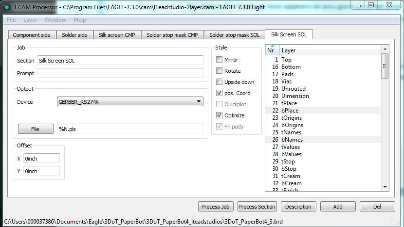
- If you look at the tabs, you will see that you don’t have a file for silk screen bottom. For simple boards, the silk screen is usually on the top layer so that you don’t need the bottom. Some of the cheap circuit board manufacturers don’t even allow bottom silk screen. But if you need silk screen on bottom layer as well, follow these steps:
- Click “Add”
- Change Section to something like “Silk Screen SOL”
- Change File to “%N.pls”
- Deselect all layers
- Select layers (see Define Silk Screen Layers). For my board I selected 22 “bPlace” and 26 “bNames”
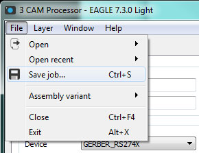
- Save the new job description with a descriptive name like Iteadstudio-2layer
If you follow instructions you will not generate the silk screen component side (*.plc file). To solve this problem process job before you get to step 3. This generates all the files except the Silk screen, solder side (*.pls file). Follow step 3 guidelines to generate everything again except in this case the .plc file which you already created so you have all 9 files needed.
They now recommend you view with a gerber viewer. I chose the one recommended by Advanced Circuits, which is here.
