Lab 0 – Line Sensing QRE1113 Reflectance Sensor
Table of Contents
Overview
By Miki
IR sensors are commonly used in robotics to detect obstacles and for line following applications. We are using IR sensors for our robots to detect the lines along the 2D maze surface. If our robots can detect a range of grayscale values, so they can navigate the maze. With our current parameters, the IR sensors cannot detect a large range of grayscale values (i.e. low resolution detection).
Goal: Design a circuit that maximizes the resolution of the IR sensors for our robots to navigate through the maze.
The QRE1113 sensor consists of an IR emitting photo diode and an IR sensitive phototransistor. The photodiode emits IR light that gets reflected back to the sensor when an object is in the light’s path.
.
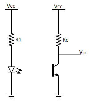

The phototransistor inside the sensor detects the reflected IR light. The base of the phototransistor is open (not connected – floating). When the reflected IR light enters the base of the phototransistor, the light is converted into a base current that controls the collector current of the transistor (EE330 comes in handy here).
The intensity of reflected IR light determines the curve for the current flowing into the collector, as shown in the following graph (Ic vs. Vce). When the intensity of reflected IR light into the base increases, the collector current will increase (i.e. move to a higher curve).
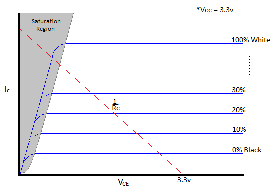
We then place a load line across the graph. The load line represents Vce, the voltage across the
transistor (from collector to emitter). This is the voltage that is read by the ADC in the microcontroller.
We can derive the load line using simple KCL:
Solve for to get the equation of the load line:
In order to maximize resolution, we need to choose the best load line. We therefore need to design a circuit that uses the best value for Rc.
Here is link to the QRE1113 Miniature Reflective Object Sensor used in the SparkFun Analog (Figure 1) and Digital Line Sensor Breakout boards. Here is a short tutorial on the Line Sensing QRE1113 Reflectance Sensor + Arduino , which explains the difference between the Analog and Digital signal conditioning circuits used with the QRE1113. In this lab we will breadboard the “discrete” version of the SparkFun breakout board as shown in Figure 2.
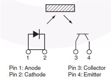
Figure 1 QRE1113 Miniature Reflective Object Sensor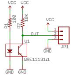
Figure 2 Schematic of SparkFun Analog Line Sensor
Experimentally it has been shown that resistors R1 and R2 used in the Sparkfun “Analog Line Sensor” circuit (Figure 2) do provide a linear output across a uniform grayscale. One of the objectives of this lab is to experimentally determine the optimal resistor values for R1 and R2. To accomplish our objective we will conduct a series of experiments.
From Figure 3 below we see that there are four (4) independent variables
1. Grayscale target
2. Distance to target (variable d )
3. LED current (variable IF )
4. Phototransistor bias (DC load line)

Figure 3 Experimental Circuit
Lab Supplies
● QRE1113 Miniature Reflective Object Sensor (provided)
● 47 ohm resistor and Set of Resistors
● Multi-turn variable resistor – anything above 100 ohms and less than 1K ohm
● Mini , half, or normal breadboard with Jumpers
● Multimeter
● Cables with alligator clips for ECS-314 lab equipment
● Large Post-it Notes or Yellow Pad (may be provided)
● Large Binder Clip(s)
● Hole punch and/or X-Acto knife, a steel ruler, and a cardboard surface to cut on. ( See Note 1 )
● Micrometer (optional)
● Sparkfun ATmega32U4 Pro Micro – 3.3V/8MHz , Arduino Leonardo , or Arduino UNO.
Note 1: One group will be running the labs in ambient light. This group not need the a hole punch or X-Acto knife.
Arduino Code
//Code for the QRE1113 Analog board
//Outputs via the serial terminal – Lower numbers mean more reflected
int QRE1113_Pin = 0; //connected to analog 0
void setup () {
analogReference(EXTERNAL);
Serial.begin (9600);
// See Note 2
}
void loop () {
int QRE_Value = analogRead (QRE1113_Pin);
Serial.println (QRE_Value);
}
*Source: Line Sensing QRE1113 Reflectance Sensor + Arduino
Note 2: As shown in Figure 3 “Experimental Circuit” the circuit is powered from a 3.3v source (Vcc = 3.3v). If you are using a 3.3v Arduino (3DoT or ProMicro 3.3v/8MHz) then no action is required. If you are using a 5v Arduino then power the circuit from the 3.3v output pin and wire a jumper from 3.3v through a 5kΩ resistor to the AREF input pin. Make sure to include the resistor, or you will risk potential damage to the microcontroller. In addition before taking any measurements be sure to set the reference voltage to AREF. This AREF voltage must be present at the reset of the microcontroller and remain the same throughout the experiment. In other words, AREF cannot be set dynamically. Consequently, all analog measurements with be taken with the reference voltage set to 3.3v.
Information about using the analogReference() function can be found here.
Arduino Output using Serial Monitor (Print) and Serial Plotter
.
Excellent Video tutorials on Arduino Print function ( Part 1 and Part 2 ), analogRead ( Part 1 and Part 2 ). Here is documentation on using the Arduino Serial Plotter (Arduino IDE versions 1.6.7 and later).
● Arduino Forum
● Instructables
Bonus Points: You may want to also export your data and plot in Excel or Matlab.
The QRE1113 Sensor Jig
Details
This device was first designed by Roy Benmoshe. It has two main features that make it useful during this lab. First, it blocks out almost all ambient light that could get between the sensor and the surface and possibly skew data results. Its second purpose is to provide a simple, consistent means of adjusting the sensor’s height.
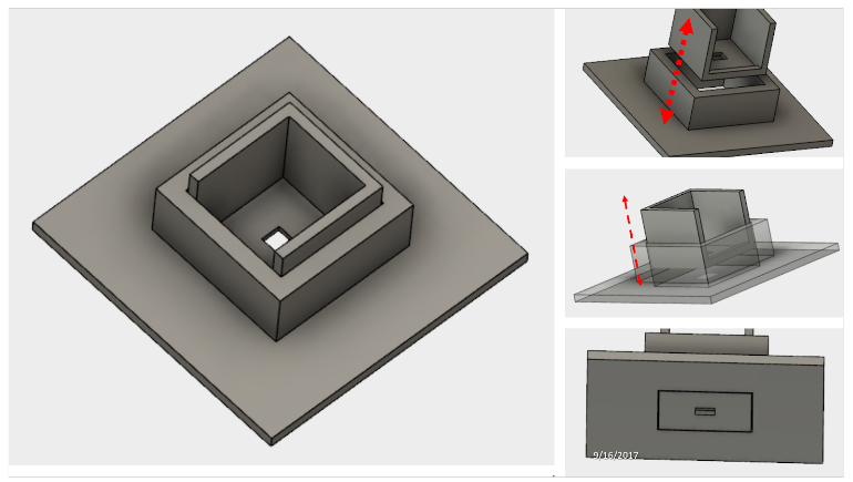
The jig consists of a baseplate supporting a square column. A smaller, four-sided cube slides inside the column. From the picture above, we can see how the cube is able to be slide up and down within the cutout while remaining level. The QRE1113 reflective sensor is positioned so that its viewing window is directly over the small hole in the bottom of the cube.
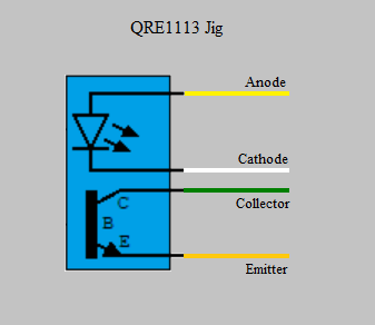
The sensor has been permanently “potted” inside the square column leaving only four wires exposed. Below the wiring diagram for the jig can be seen.
WARNING: Inaccurately connecting the wires to your circuit could permanently damage and/or destroy the sensor. The voltage source powering your sensor should be 3.3v, NOT 5v. Also be sure to check that you have placed a limiting resistor ( at least 47Ω) in addition to your potentiometer between Vcc and the anode of the LED before any power is introduced to the circuit.
Use
- Place the baseplate onto the testing surface with the sensor facing down
- With the sensor connected to your circuit, slide the small cube containing the sensor into the baseplate (see top right picture above) until both bottom surfaces become flush. Note that the top of the cube will still sit slightly above the top surface of the baseplate (see left picture above).
- Adjust the height of the sensor by sliding the small cube away from the testing surface in 0.2mm increments.
3a. This can be done multiple ways however, the easiest way we found was to cut a square section (roughly 1.5 cm X 1.5 cm) out of an entire standard pad of sticky-notes. Note this section must be smaller than 2 cm X 2 cm, so it can fit inside the square column.
3b. This sticky-note pad can then be placed between the small cube that houses the sensor and the testing surface. You can then push slightly on the baseplate, so its bottom face returns to the testing surface and the cube is displaced the exact distance of the sticky-note pad thickness.
3c. Once the cube has been displaced to the appropriate height, the sticky-note pad is removed and, due to the friction between the cube and the baseplate, the displacement distance will remain the same.
3d. The distance of the displacement (i.e. distance between the sensor and the surface) can be adjusted by peeling off a predetermined number of sticky-note sheets (1 sheet ≃ 0.09 mm). For this reason it would most likely be easiest to start with the maximum height desired (5 mm) during the test, then peel off sticky notes in 0.2 mm intervals until the minimum desired height was reached.
Experiment 1 – Optimum Distance to Target
.
1. Grayscale target – White Paper
2. Distance to target – independent variable [0.2mm steps, 0 – 5mm ]
3. LED current = 20 mA
4. Phototransistor bias (DC load line) = 10K
Experimental Setup
As discussed in lab. You will need the following.
● Notebook paper
● Voltmeter and variable resistor – record voltmeter accuracy
● Arduino microcontroller board (3DoT, Sparkfun ProMicro 3.3v, Leonardo, Uno)
Important Notes:
- As shown in Figure 3 the circuit is powered from a 3.3v source (Vcc = 3.3v). If you are using a 3.3v Arduino (3DoT or ProMicro 3.3v/8MHz) then no action is required. If you are using a 5v Arduino then power the circuit from the 3.3v output pin and wire a jumper from 3.3v to the AREF input pin.
- All experiments should not allow room lighting to reach phototransistor.
Experimental Output
For each experimental step d = 0 – 5mm, in ≃ 0.2mm steps take readings using a voltmeter and as read from the Arduino serial output port (analogRead ).
Solving the equation provided in the Analog-to-Digital lecture and provided here for VIN , convert the Arduino ADC output (units are a Digital Number – DN) into its corresponding voltage ( VIN ).
, where
= 3.3v
Using Ohm’s law, and measured value for R2 (≃ 10KΩ), calculate Ic . On one graph using two different notations (ex. X = Voltmeter, O = Arduino) plot your experimental results. Using Excel, Matlab, etc. curve fit your experimental results for both sets of readings (again on a single plot). Your resulting plot should take the form shown in Figure 4. Differences from this figure include IF = 20mA, VCE = 3.3v, TA = measured; Two plots (Voltmeter, Arduino) and no “Mirror” plot; Actual current (not Normalized).
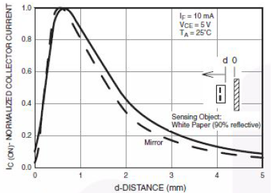
Figure 4 Collector Current vs. Distance between device and target
Based on team assignment set d = [Optimum, 1, 2, 2.5, 3, 3.5, 4] mm
Experiment 2 – Optimum LED Current and R1
.
1. Grayscale target – White Paper
2. Distance to target d – Based on team assignment
3. LED current = independent variable IF = 0 – 40 mA, in 2 mA steps
4. Phototransistor bias (DC load line) = 10K
As in most engineering problems there is a tradeoff to be made. In this case we want to use the minimum amount of power, while also achieving the best resolution possible.
Experimental Output
For each experimental step IF = 0 – 40 mA, in 2 mA steps take readings using a voltmeter and as read from the Arduino serial output port (analogRead). Following the procedures outlined in Experiment 1, create a plot, which should take the form shown in Figure 5. Differences from this figure include Two plots (Voltmeter, Arduino).

Figure 5 Collector Current vs. Forward Current
As an ancillary objective measure the forward voltage ( VF ) drop at different forward current values ( IF ). For each experiment record the room temperature.

Figure 6 Forward Current vs. Forward Current
Based on IF current assigned [5, 10, 15, 20] to the team find R1
Experiment 3 – Optimum R2 based on Team Assignment
.
1. Grayscale target – White Paper
2. Distance to target d – Based on team assignment
3. LED current IF – Based on team assignment
Experimental Objective
One of the key objectives of this lab is to experimentally generate Figure 4 “Collector Current vs. Distance” between device and target and Figure 8 “Collector Current vs. Collector to Emitter Voltage” as shown in the QRE1113 Miniature Reflective Object Sensor datasheet.
The characteristic curve for the Phototransistor (Figure 8) will be generated from a gray scale as provided here. Base on experimental results you may be required to focus on additional gray scale images.
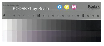 Figure 7 Sample Gray Scale Page
Experimentally, once an optimum distance has been experimentally determined, the transistor characteristic curve will be generated using a load line for each gray scale target (see Figure 9 ”Sample transistor characteristic curve with load line”).
Figure 8 Collector Current vs. Collector to Emitter Voltage
Use the above information and your EE330 “Transistor Characteristic Curve Lab” to complete this lab. As before please collect data using a multimeter and your Arduino.
Based on experimental results calculate R2
Reference Lab Experiments
● Photo Transistor Characteristics by Dr. Gabriel M. Rebeiz
● Lesson 1452, Optoelectronics Experiment 6, Photodiode and Phototransistor Current Measurements
● http://inst.eecs.berkeley.edu/~ee105/sp11/labs/Lab3.pdf
● http://archivio.iav.it/Doc/Vanni_Paolo/5CNT/EE332LE1rev3.pdf
Lab Report
Introduction
The introduction essentially summarizes the entire experiment. It defines the purpose of the lab and explains the goals and/or what one is trying to learn in the process. It should also present any concepts (scientific theories, previous experiments etc.) that act as background information, which would be crucial to understanding the lab.
Materials/Setup
This section should, as the name implies, include a list of all materials used to complete the lab. It will also explain how each of these items were prepared in order to obtain the results of the experiment. It is important to be as detailed as possible here, both to eliminate procedural ambiguity and to increase the lab’s ability to be reproduced.
For this lab specifically, all three experiments will share a materials section however, each will have its own setup procedures. Also, many students have found it easier to include pictures of their setup with only a brief description.
Discussion
The discussion is the main section of the lab report, where the data from the experiment is presented and both it and the lab itself are reviewed. This includes any challenges encountered during the procedures, as well as reaction to the data. Interpretations of the results themselves should be avoided in this section, and discussion should instead be limited to answering questions such as how successful the experiment was and how the data compared to the expected outcome.
In this specific lab, experimental data must be presented using graphs. Since there are three separate parts to this experiment, there should also be three subsections under the main discussion section, each presenting its corresponding data. Graphs can be generated in a number of ways however, the most common forms seen in this class are MATLAB and Microsoft Excel.
Conclusion
The conclusion section elaborates on the claims made during the discussion. It seeks to provide an explanation as to why the results appear the way they do, and whether or not they make sense in the context of the initial goal of the experiment. It is important to state if the goal was achieved, as well as what was learned during the course of the lab.
Appendix
The appendix section is where all code used during the lab should go. For this experiment, that includes both the Arduino code for reading the sensor, as well as any code used to generate the graphs (MATLAB, Python etc.). Each block of code should have a corresponding subsection within the appendix. For example, all of the Arduino code might be labeled as subsection “A”, while the entire MATLAB code could be labeled as “B”.
.
.
Lab 0 Deliverable(s)This lab requires a full, written lab report. Only one report per team is required, which will be submitted via the “Dropbox” folder in Beachboard. The outline and requirements for this report can be found above in the section labeled “Lab Report”. All lab reports should represent your own work – DO NOT COPY. |
Checklist
- Your lab report follows the format listed above under the “Lab Report” section, including an abstract, introduction, materials/setup, discussion, conclusion and an appendix
- Graphs have been generated for each of the three experiments
- A graph of “IC vs VCE” is included
- A graph of “IC vs Distance” is included
- A load line is included on the appropriate graph
Appendix
Appendix A – Source Material

Figure 9 Normalized Collector Current vs. Collector to Emitter Voltage

Figure 10 Sample transistor characteristic curve with load line