Mini-Rosco/Spring/2020
Mini-Rosco: PCB Design Process
Author/s: Giann Carlo C. Bullo
Table of Contents
Introduction
This is the PCB design process for Mini-Rosco shield. The shield consists of a GPS module, ultrasonic sensor, and a magnetometer that will act as a compass. It will be used due to limited I/O pins that are available on the 3Dot. The design of this PCB will be compatible for the 3Dot.
Bread Boarding
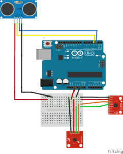
In order to implement the follow and way points aspect of the project, Mini-Rosco would need to utilize a GPS module and ultrasonic sensor. The GPS module would be connected through I2C pins while the ultrasonic would repurposed the MOSI and MISO pins as trig and echo since Mini-Rosco will not be utilizing SPI serial communication. The first iteration only consisted of the GPS module and ultrasonic sensor. We believed that the GPS would be enough to implement way points. Through testing, however, we realized in order to have accurate heading for the robot to move toward the designated way point a magnetometer was needed. This magnetometer would act as a compass and provide the robot with x y and z headings. The fritzing diagram above represents a breadboard version of the PCB we are creating. The original bread boarding was done with the Arduino Uno for the GPS module tracking and the 3dot for the motor movements for V1 demo. V2 demo would fully implement the 3Dot using the GPS Module. The initial bread boarding was successful proving the design works.
First Iteration
Since we proved that the circuit works as intended, I started the design and of the custom PCB as required. The design we needed to build was fairly simple, so after following through Arxterra’s Eagle guide provided I set out designing it.
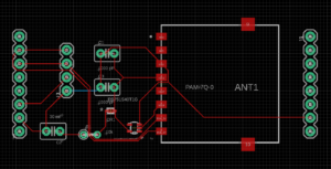
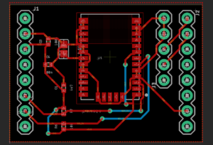
The first iteration consisted of using the same GPS module that was used on the breakout board in testing. This was the PAM 7Q which had UART and I2C communication. To implement the ultrasonic sensor I added a 4 pin connector and connected it to the I2C pins. We chose to get an ultrasonic sensor that communicates through I2C because the group decided to use multiple sensors for better tracking. Since I had little experience with Eagle CAD I connected most of the pads using only traces and vias. While creating the first iteration, I did not focus on the dimension but rather how to connect each pad and make sure I had an idea of the design I wanted to implement.
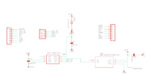
To create a board I referenced the Parallax breakout boards schematic because it did not come with any Eagle CAD files. I determined which parts were not needed and what parts were essential. Most of the breakout boards were not needed. For example the signal conditioning for RX and TX did not need to be implemented because we were only going to use its I2C pins. After researching what parts were needed I created the board and sent it to Chris so he may check the board.
My first iteration of the PCB and Schematic had many errors. For example the components that are used such as the resistor and capacitors needed to be surface mounts and not through-hole. It was through these emails that we found a very huge error in our board. Looking through the datasheet we found that the Pam 7Q was already a PCB in itself. This would render our custom PCB useless as it will only need pin connectors for the GPS itself.
Second Iteration
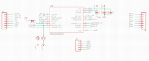
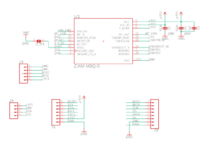
As I continued to email Chris for advice we found a solution to our GPS module problem. Through some research I was able to find a replacement GPS module that was a surface mount. I also found a breakout board using this module to use as reference. Luckily this board had Eagle Cad files for me to use. Just like the first iteration I looked through the datasheet and schematic to determine what parts are needed.
In creating this board I mostly used traces and vias to connect the pads. I was advised to create a ground pour since there were a lot of ground pins. Creating a ground pour would help make the board a lot cleaner in terms of design. I also fixed up the dimension to make sure that the new GPS module will fit on the shield. I also increased the size of some traces to have a better connection.
Although my second iteration improved I still had many errors. The first error was that some parts of the schematic were not even connected. Although I created a net either the naming did not match or it looked connected but was not. The second error was the pull up resistors on the SDA and SCL pins. Professor Hill informed me that these pins on the 3dot already have pull up resistors so they are not needed. The final error was that the dimensions and one of the shield connectors was reversed. This means that the whole layout needed to be redone. With the help of professor Hill, he was able to help clean up my schematic and a blank shield for me to use. I used this cleaned up schematic to create a new layout on a blank shield.
Final Iteration
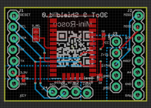
For the final iteration I referenced professor Hill’s layout that he cleaned up. First I created a ground pour on the top of the board to make it easier to connect to ground. I then created traces according to the schematic utilizing vias and making sure that the ground pour would reach the whole board. In addition to the ground pour I also made a VCC pour in order to simplify the amount of traces needed. I created the pour targeting only the pins that were +3V3.
As we were preparing for V2 our group decided to change our ultrasonic sensor. The reason for this is because the HC-SR04 only uses 5V this means we would have to implement level shifting for the voltage. Another reason is that instead of using the I2C pins we will be re purposing the MOSI and MISO pins as UART and connect the ultrasonic so it will move via the pan system. We decided to use the US100 because it can be connected via UART and works using 3V-5V. Another change we made was to add a compass in order to get better headings for the way point aspect of our robot. To do this I added 4 pin connectors so I can connect it through the shield. We had to do this in order to minimize the interference that the GPS module can have on the compass.
While working on the board the widths of all traces became 10 and I avoided creating 90 degree angles for these traces. I also retraced some connections in order to connect to the center of the pad. I was advised to start at the pad in order to snap to the center. A lot of the editing was on the SDA and SCL traces to make sure that the pores would reach ground and VCC.
Conclusion
Overall the PCB design proved to be successful. The PCB was manufactured from JLCPCB website and soldered together using capacitors and the GPS module. I have learned lot more from Hill in terms of layout and board customization. It has helped me learn a new skill that can be applied for future work and jobs.

