Fall 2016 Biped – PCB layout
Designing the PCB
By: Hector Martinez (Manufacturing)
Approved by: Ijya Karki (Project Manager)
Table of Contents
Introduction
Once the schematic design is complete by E&C engineer, Allen, it is time to design the PCB layout. The PCB layout needs to have a thought out design that will work logically and seamlessly with our project. Since our PCB will be a shield for the 3dot board, we also have to consider the dimensions of the 3dot board as well as space allocation.
Process
There are a lot of resources online that will explain how to layout a pcb, but one crucial bit of advice that I received came from our president Fabian, he suggested I start by grouping all the components that work together.

Fig. 1 – New PCB project based on Schematic layout.
For example, our SX1509 GPIO expander contains a decoupling capacitor at the power input and 3 resistors that will work with our color sensor, by grouping those components together you begin to think about how and where these groups of components will be placed.
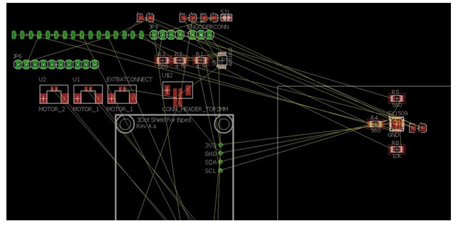
Fig. 2 – Grouping of SX1509 and its attributed components.
As you continue to group all your components you begin to realize that some groups must be place at specific locations. The picture below shows the connectors for motor1 and motor2 are connected directly to the board at A and B. Additionally, since we will be using an external battery the LM1048IS that we will use to regulate that voltage must be close to the EXT battery connection towards the bottom of the board along with all its components.
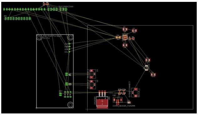
Fig. 3 – Continuing to group components you realize where some components must go.
Tracing
Once you are done grouping, the tedious job laying down traces to connect all your components. You may choose to place some of your smd components on the underside of the board or leave everything on one side. When you begin to trace, you want to try and route all your traces on one side, once you are unable to do this without traces overlapping, you can take advantage of Vias and placing traces on the other side of the board.

Fig. 4 – Grouping complete, time to lay down traces. The blue component is the SX1509 on the underside of the board, this is done when space is limited.
Clearly, we have plenty of space to fit all of our components on one side of the board. Once the traces have been placed you may opt to go through and make all text on the silk screen the same dimensions. This makes your board visually appealing and will help when it is time to solder.
Conclusion
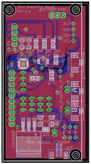
Fig. 5 – You are done!
The image above shows red and blue traces that connect all components together, each is on opposite sides of the board. The planes is red or blue are grounds, these are meant to protect the board from noise, etc. Once you are done, you can admire your work.