Fall 2016 Velociraptor (W): PCB Layout
By: Aaron Choi (Manufacturing Engineer)
Edited and Approved by:
– Lam Nguyen (Project Manager)
– Tim Haddadian (Division Manager for Manufacturing Engineer)
Table of Contents
Requirements
L 1-9 requirement states the Velociraptor shall have an external PCB with an I2C interface which will be similar to the 3DotBoard
Introduction
To fulfill the Level 1-9 requirement, a layout of a custom PCB with Surface Mount Technology (SMT) discrete components will be implemented. This layout will be created through EagleCAD. Once the layout is carried out, approval must be given from Professor Hill or the class President Fabian Sasuke.
Design
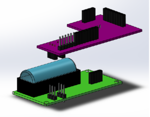
The design of the PCB layout revolved around the physical dimensions of the 3DotBoard. The idea is to place the custom PCB above the 3DotBoard. Female pin headers of the PCB will connect to the male pin headers on the 3DotBoard. The battery of the 3DotBoard limits the vertical distance from the PCB to 3DotBoard. This would affect the type of pin headers and connectors used. To avoid the physical constraints, the PCB shall have an L-shape, leaving room for pin header connections to connect properly.
Diagram 1: The figure above shows the SolidWorks model of our PCB.
For the placement and wiring components, rules were carried out following guidelines and tutorials from SparkFun [1] and Professor Hill’s PCB training [2]. The wires were set to a 45 degree angle, the decoupling capacitors were placed close to the IC components, and none of the wiring overlaps.
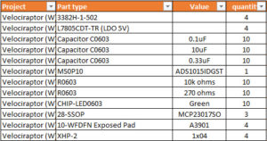
The placement of the IC components were prioritized on the top layer. The reason for this was to utilize a SMT solder paste stencil for only the top layer. However, due to wiring, one of the IC components were placed on the bottom layer. The IC component placed on the bottom layer shall be hand soldered and utilizing a heat gun. The parts list chosen are given in Table 1 below.
Table1: Parts list ordered from DigiKey.
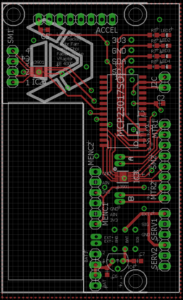
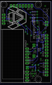
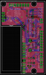
The final PCB layout is given below.
Diagram 2: The Top Layer wiring of the custom PCB.
Diagram 3: The Bottom Layer wiring of the custom PCB.
Conclusion
Diagram 4: PCB layout with ground planes.
Diagram 4 shows the final PCB layout for the custom PCB design. The custom PCB will be powered by 7.4V external Li-Po batteries. To bring down the voltage, a LDO was incorporated within the PCB. Stepper motor drivers were implemented for the linear actuators, which are micro stepper motors. The connectors for the IMU MPU-6050 were pin headers so that the MPU-6050 can simply be connected to the pin headers without any soldering. After running the Design Rule Check (DRC), no errors were found. The PCB will be ordered from OSH Park and an OSH Park DRC will be carried out.
References
[1] https://learn.sparkfun.com/tutorials/using-eagle-board-layout [2] http://web.csulb.edu/~hill/ee400d/Technical%20Training%20Series/11%20PCB%20Layout%20with%20Eagle%20CAD%20(Working%20Stencil%20Addition).pdf

