Assembly Robot Prelab 4 – Working with Timers and Delays
Table of Contents
Introduction
The focus of this prelab is to help you understand how the timers operate and prepare you to write the code needed to configure them for a specific delay.
Basics about Timers
As discussed in lecture, there are several ways the microcontroller can keep track of time and be programmed to execute specific actions after a delay. It can be done with a loop that has been designed to use up that amount of time or handled by a separate system. That is where the timers come in. They are configurable counters that can be set up for a wide range of applications such as:
- Turn on or turn off an external device at a programmed time.
- Generate a precision output signal (period, duty cycle, frequency). For example, generate a complex digital waveform with varying pulse width to control the speed of a DC motor
- Measure the characteristics (period, duty cycle, frequency) of an incoming digital signal
- Count external events
All of these functions are done manually or automatically depending on how the timer is configured. The ATmega32u4 has four timers in total. Timer 0 is an 8 bit timer, Timer 1 and 3 are 16 bit timers, and Timer 4 is a 10 bit high speed timer.
Important Terminology
Before we get into the calculations and configuration, there are some key terms to understand.
Frequency
The number of times a particular event repeats within a 1-s period. The unit of frequency is Hertz, or cycles per second. For example, a sinusoidal signal with a 60-Hz frequency means that a full cycle of a sinusoidal signal repeats itself 60 times each second, or every 16.67 ms. For the digital waveform shown below, the frequency is 2 Hz.
Period
The flip side of frequency is the period. If an event occurs with a rate of 2 Hz, the period of that event is 500 ms. To find a period, given a frequency, or vice versa, we simply need to remember their inverse relationship, where F and T represent a frequency and the corresponding period, respectively.
Duty Cycle
In many applications, periodic pulses are used as control signals. A good example is the use of a periodic pulse to control a servo motor. To control the direction and sometimes the speed of a motor, a periodic pulse signal with a changing duty cycle over time is used.
Duty cycle is defined as the percentage of one period a signal is ON. The periodic pulse signal shown in the Figure 1 is ON for 50% of the signal period and off for the rest of the period. Therefore, we call the signal in a periodic pulse signal with a 50% duty cycle. This special case is also called a square wave.

Figure 1: Digital Waveform
One key thing to keep in mind here is that the amount of time that the signal is HIGH can vary from the amount of time that it is LOW depending on the duty cycle. For figure 1, they are the same. This allows the programmer to use the same delay to generate this signal on an output pin. Due to this, the delay to configure the timer for does not always match with the period of the desired signal.
Timer Register Descriptions
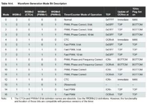
With the terminology covered, we can now focus on the timer registers that you will be working with in the lab. As mentioned earlier, there are many ways that the timers can be used as shown in Figure 2. It is important to note that these registers are not part of the general purpose registers that are in the AVR CPU. They are located within the Extended I/O registers which are a part of the SRAM address space, not the I/O address space. We are only concerned with the normal mode which will increment by 1 until it reaches the maximum value 0xFFFF and then restarts at 0x0000 when it overflows. You may notice that there are terms for TOP, BOTTOM, and MAX. These can be changed depending on the operating mode but you should consider MAX to be 0xFFFF and BOTTOM to be 0x0000 for our course.
As we are only working in normal mode, you will not need to modify any of the configuration registers besides TCCR1B which stands for Timer/Counter 1 Control Register B. This is because the default setting for the other registers is to start in normal mode.
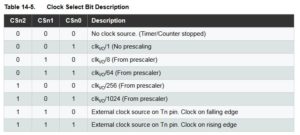
The main bits that we are concerned about in TCCR1B are the clock select or CS bits. These bits allow us to define how quickly the timer will increment and ultimately how long it takes to overflow. The options for this are all based on the system clock signal coming from the microcontroller or an external clock source as indicated in Figure 4. You will need to select the appropriate combination for the bits in order to configure the timer for your desired delay. For example, if the pre-scale value of 256 is chosen with a system clock frequency of 16 MHz, the clock frequency for the timer will effectively be 62.5 KHz and result in a maximum delay of 1.0486 seconds.
The last of the registers that you will need to become familiar with are the timer counter registers (TCNT1H and TCNT1L) and the timer interrupt flag register (TIFR1). They are relatively self explanatory, with the timer counter registers holding the current value before the next increment and the timer interrupt flag register holds the status of the flags. We are mainly concerned with the TOV1 bit which indicates if the timer has overflowed (becomes 1) or not. One important thing to keep in mind is that the timer does not automatically tell the microcontroller that the overflow has occurred unless the corresponding interrupt was configured. If that has not been set, the microcontroller will only know that the timer is finished when it is programmed to check the value of the TOV1 bit.
Calculating the values for a specific delay
Maximum Delay
So can TCNT1 generate the 250 ms delay required to generate our 2 Hz square wave? To answer that question, we will need to determine the maximum delay possible. Assuming a system clock frequency of 16.000 MHz and a pre-scale divisor of 64, the largest time delay possible is achieved by setting both TCNT1H and TCNT1L to zero, which results in the overflow flag TOV1 flag being set after 216 = 65,536 tics of the Timer/Counter1 clock.
fT1 = fTclk_I/O/64, given fTclk_I/O = fclk then fT1 = 16.000 MHz / 64 = 250 KHz
and therefore T1max = 65,536 tics / 250 KHz = 262.14 msec
Clearly, Timer 1 can generate a delay of 250 msec. Our next step is to calculate the TCNT1 load value needed to generate a 250 ms delay.
Step to Calculate Timer Load Value (Normal Mode)
To generate a 250 msec delay assuming a clock frequency of 16 MHz and a prescale divisor of 64.
Variables
tclk_T1 – Period of clock input to Timer/Counter1
fclk – AVR system clock frequency
Solution
- Divide desired time delay by tclk_T1 where tclk_T1 = 64/fclk = 64 / 16.000 MHz = 4 µsec
250msec / 4 µs = 62,500 - Subtract 65,536 – step 1
65,536 – 62,500 = 3,036 - Convert step 2 to hex.
3,036 = 0x0BDC
Questions
Question 1 – Calculate the maximum delay that can be generated with Timer 4 when the system clock frequency is 16 MHz and the selected pre-scale value is 256. Keep in mind that the number of bits used for Timer 4 and and time for each count/increment is needed to solve this problem.
Question 2 – Calculate the value to be loaded to the Timer 0 Counter Register in order to have a delay of 218 microseconds if Timer 0 is used with a system clock frequency of 20 MHz and a pre-scale value of 64.
Question 3 – Calculate the value to be loaded to the Timer 3 Counter Register in order to have a delay of 2.43 seconds if Timer 3 is used with a system clock frequency of 16 MHz. The pre-scale value is not given and must be determined. Make sure to select the lowest value possible that will work.
Question 4 – Write the lines of code needed to implement the configuration listed in Question 3. Keep in mind that the names of the registers for the timers is exactly the same except for the timer number. IE TCCR1B vs TCCR3B.
Prelab 4 Deliverable(s)
Page 1 – Title Page with Name, lab title, and photo
Page 2 – Answers to questions. Make sure to show all of the work involved with getting to the answer.


