Spring 2018 AT-ST Custom PCB Layout/Design
By: Shweta Hebbalkar (Electronics and Controls – Hardware)
Verified By: Intiser Kabir (Project Manager)
Approved By: Miguel Garcia (Quality Assurance)
Table of Contents
Introduction
For the AT-ST project, one of our goals is to create custom PCB using Eagle software. This software allows the user to generate PCB layouts, in order to use the Eagle software I need to learn how to use the software. With lack of experience using the Eagle software previously, it took me a week to two weeks to learn the general concept. So overview of the concepts is learning a PCB, also it is most common named “printed wiring board” or “printed wiring cards”. So it is a board that has lined and pads that connect various points together.
Transformation #1
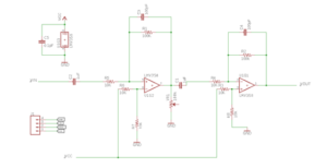
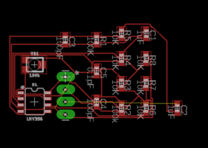
The first thing I ever built in the Eagle CAD is the flowing figure, a schematic and PCB layout. In the figure one the schematic is for the op-amp amplifier I followed this schematic from the workshop that was directed by Chris and others. Creating the PCB layout was easy to follow basically I moved all the components into the black box and then AutoRoute the trace.
In the picture above, there are traces that electrically connect the various connectors and component to each other. A PCB allows signals and power to be routed between physical devices.
Transformation #2
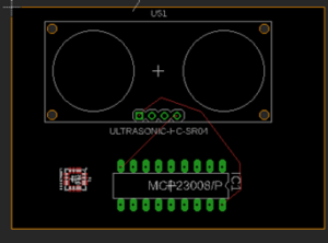
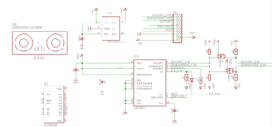
After two weeks of refining my skill in Eagle CAD with help of the Chris and others at the workshop. I was finally started designing my very first custom PCB layout schematic. When I was designing the circuit, it took me four days to find the library that I need it to create the custom PCB layout. Eventually, I was successful to get all the all the library that I need it, for example, the ultrasonic sensor the gyroscope and i2c expander as shown below in schematic and the board.
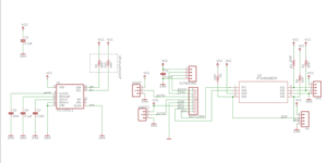
In fig 4 the schematic was just placed on the template thinking that they will be all connecting in the board.
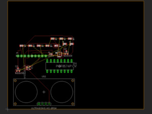
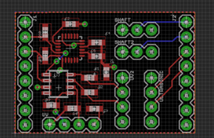
In Fig 5 the board layout, I placed all the components in the black box and then arranged in preferred to make it in compact space due to requirement. Afterward, I try to route the i2c expander with an ultrasonic sensor. In conclusion, from these we all understand that I need more practice then I thought and also need more clear instruction as well.
Transformation #3
In order to send in the custom PCB layout to print, I have to illustrate my board to get approval from our Customer. Which is very useful because professor Hill helped me the lot to make my board even more efficient. For example, the routing line has to be the 45-degree angle and it should be the clean line. If I am using polygon plane the top one supposed to be ground and the bottom one should the source. Always make sure to have the right parts if not then I redo the board design. According to the team consensus, we decide that we are going to make our PCB as the front shield.
Though this images below is my final version before getting approval. I had to go through many iterations. I had to connect all the lines in the schematic and I have to make it look easier to read for others.
Unfortunately, we did not inform our professor that we are changing our custom PCB from top shield to the front shield. Still, the images above and I went with and I design our PCB. Then After emailing professor this board to get approval from our professor however he emailed me back saying that why am I using the front shield. Then I respond to him saying that we need to use the analog pin, therefore, we are using the front shield. However, the professor said we don’t need to use analog pin we need digital pins and that pin is given in the top shield so I have to redo the custom PCB again.
In conclusion, we did not inform the customer beforehand with my design. Which means that I need I made myself double the work. The more time I spent with design PCB, I became more cautious because we would have to save time and print the board right away because printing board takes a lot of time.
Transformation #4
After getting some feedback from Customer, I already lost a big amount of time, which means that I get to have less time printing board, however, I started designing the top shield. With many changes like the routing and the get the right parts package size for schematic chaining any specifications according to professor liking I get approval the image below.
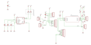
This is schematic is final schematic after many variations.
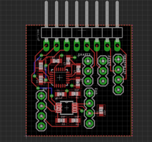
The final PCB board that we send it to OSHPARK to print.
Maintaining low expectation with my first board design because they had lots of problems and the final was my 25th board design that had the fewer error. The schematics are important and trying to design a board with a good schematic in place first is an exercise in futility.
In conclusion, I have learned lot more from Hill then division manager although they were helpful, mostly it is our job own responsibility to learn the eagle software.
