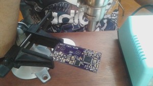
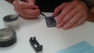
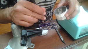
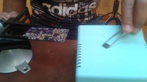
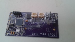
Spring 2016 3DOT Goliath, PCB testing

By: Kevin Moran (Electronics and Control Engineer)

Once the PCB was assembled by the manufacturing engineer (Jerry Lui), it was to test it. If all the testing and assembling had been done correctly then the PCB should have worked with a problem. As testing began we quickly realized that the PCB was not sending any voltage to the IR emitter. With the help of Jeff Cool, Tae Le, and Jerry Lui, we realized that the problem was with the NPN transistor we had ordered.

1


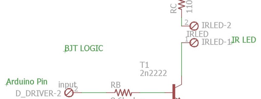
The problem was with this 2n2222 transistor above. The RB was not being used as a base, but rather the collector (which should be connected to ground). After many attempts, we came to the conclusion that the SMD transistor had been placed wrong.


2

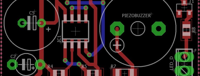
As can be seen by the arrow, once we compared the diagram of the transistor, with this picture, we realized that the resistor RB was going to the right connection of the transistor, when it should have been pointed to the left connector, and the right connector straight to ground. Thanks to the ingenuity and quick thinking of Jerry Lui, he was able to quickly fix this problem, by flipping the SMA transistor over. After that was fixed, we tested the IR emitter and we saw voltage going through it, and the receiver worked perfectly as well. Below is the final output of the PCB, converting an analog signal into a single bit digital signal! YAY!

3


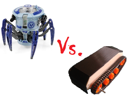
As can be seen, a perfect digital signal with either a 0 or 1 bit. On/off applications. Now we are ready to defeat the 3DoT Spider bot.


Sources:

http://www.mouser.com/ProductDetail/TTElectronics/2N2222ACSM/?qs=%2fha2pyFaduhY4tRQXhKL%2feLyX%252bM6m2ylmJNPJCp%2fVeaSnptWjDmpSA%3d%3d


Spring 2016 3DOT Goliath, SMD Soldering

By: Jerry Lui (Manufacturing Engineer)

The reason for this post is to create a guide on how to solder SMD components onto your fabricated board.

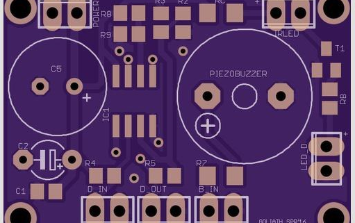
By the last quarter of the semester, custom PCB’s should have been fabricated and all components on hand. Our PCB is shown above with a total dimension of 1’’x1.425’’. The majority of the components are SMD with the exception of the 2 through hole dielectric capacitors, piezo speaker, and phoenix pins.


First the PCB should be cleaned thoroughly with at least 70% rubbing alcohol (preferably 90%+) by soaking either Kim-wipes or cotton swabs.


1


Next flux should be applied to the contacts of the board. Generally use a no-clean water based flux for ease of cleaning but a typical rosin based flux will suffice. These come in small containers to syringes to pen applicators.


2


Now that the flux has been applied each contact pad has to have solder paste or normal solder.

3


A stencil can be used but it needs to be fabricated so the next step will be hand application


4


DO NOT put too much solder paste. There only needs to be enough to thinly cover the pads. For the multi-pin packages like opamps, a thin line of solder paste can be applied perpendicularly to the pads instead applying it to each pad individually. Once all the pads have been covered in solder paste it’s time to add the components.

5


Here I use tweezers to place the SMD components onto the prepared board. To help with placing the SMD properly, grip the components from the top or use a  angled tweezer. The components don’t need to be pressed all the way down, give them a light press and the capillary effect of the solder will automatically align them.


To have a proper solder joint the board needs to be warmed up properly. An increase of  will be fine. If a reflow oven isn’t being used a hot air station is adequate as well.

6


Set the temperature to around 310C (depends on the flux paste used) with the air setting to 1~3 and hold the hot air reflow gun 3~5 inches over the board while rotating the gun for a few seconds. The point of this is to heat up the board (especially the ground plane) and to allow the components/leads to come up to the proper temperature. Once the board is warmed up (the paste will also start to become more fluid) hold the reflow gun 1~2 inches over the board while wiggling the gun. The solder will start to melt and align the components to the pads.


7


Once the board is completely soldered, clean it again with rubbing alcohol and kim wipes or cotton swabs.

8

Conclusion:

Soldering surface mount components is very straightforward and isn’t as hard as many people believe it to be, especially with a hot air gun or reflow oven. As long as you have a steady hand (for hand soldering) and patience (hot air gun) you’ll be able to solder SMD components with ease.


EEvlog has great tutorials on how to re-flow:

How to re-flow


Spring 2016 3DOT Goliath, Mission Objective Update

By:  Tae Min Lee (System)

Mission objective also known as Con Ops was needed to set the rules for the laser tag game.  Both systems engineer from the SpiderBot (Chris Hirunthanakorn) and the Goliath (Tae Min Lee) discussed and finalized the rules for the laser tag game.  The list of rules that are listed below will allow us to have a clean and fair match.

Con Ops:

  1. The game will last for three rounds. One round ends when a robot is hit three times and is disabled. This may last up to 10 or 15 minutes.


  1. A robot is considered disabled if it is unresponsive to commands for 10 seconds after the final tag.


  1. At the end of one round, both robots will return to their starting positions.


  1. The game will take place in a 6 ft x 6ft area on the linoleum floor of ECS 315. If any robot leaves the designated area, they are not allowed to attempt to tag the other robot and must re-enter the game area.


  1. An Infrared LED emitter and Infrared detector will be used as the tagging system.


  1. The maximum distance for detecting a direct hit will be 5 ft. This means the IR emitter is hitting the detector in a straight line from 5 ft away. Whatever voltage is outputted by the detector will be the minimum threshold for defining a hit. (need to define that voltage here once we figure it out)


  1. Collisions between the two robots is not allowed. If a collision does occur, the robot that caused it will take a penalty hit. Once the penalty hit is taken, the robots move back to their starting positions.


  1. A buzzer will make a noise to indicate when the robot is tagged and when it is disabled.


  1. When a robot is tagged, it will make a sound and it will be deactivated for the next 5 seconds. This will allow the robot to move out of the way and not cause multiple tags at once.


Spring 2016 3DOT Goliath, CDR Debrief

By: Ayman Aljohani (Project Manager)

Introduction:

Critical Design Review(CDR), is an important phase of the project, it presents the design of the project. It also provides a clear view on the project standing and percent completion.

After presenting our CDR, we were debriefed by the president, and the customer on our presentation content .

Here is  the debrief summary:


Title Page:

Was good, nothing to comment on.

Executive Summary

weakness:

Too much information was provided in  the executive summary

correction: 

Keep it short and simple

Only explain the major features of the project

System Design

weakness: 

Missing 3Dot Components on the System Block Diagram

Poly fuses

LDO

LIPO Charger

strength: 

Paul commented that the color coding on the system block diagram and  the legend, it was easy to follow. 

Experimental Results:

weakness:

Problem with the analog Schmitt trigger

However, Elec. Engineer, Kevin,  found out the problem and fixed the output of the threshold voltage on 4/20/2016.  The president is also notified about the fix on the threshold voltage issue.

Our goal of the Schmitt trigger is to convert analog signal to a digital signal.

Subsystem Design

No comment, it was good.

Interface Design

weakness:

messing 3DOT components.

correction:

Include 3Dot components

Custom PCB Design

weakness:

 The custom PCB  was not designed to be able to attach onto the 3Dot board as a shield.  The point of this design is to avoid the number of wires being used to connect to the microcontroller.

correction: 

Have custom PCB attach to the 4 pins on the 3Dot.

For future design reference it will follow a similar design shown by the following site:

https://www.adafruit.com/products/94

Software Design

weakness: 

The lockdown code that will disable the robot after 3 hits from the enemy was not included.

Verification & Validation Test Plans

Everything was good for the verification and validation test plans.

Project Updates

strength: 

Smartsheet is good to use  

weakness: 

 The actual cost of the free items was not included 

Fix the uncertainty for the resource report, it should be zero uncertainty. 

WBS should not have a repeated loop process

Project Demonstration

it was a good demo. 


Spring 2016 3DOT Goliath, Making Laser Tag Possible: Putting it all Together

By: Kevin Moran (Electronics and Control Engineer), Tae Lee (Systems- Provided the musical notes code needed for this game)


In this post, I will be discussing the final results for the IR Emitter when being used alongside with a Schmitt Trigger and the code that will be used to determine when the 3DoT Rover gets hit 3 times by an IR emitter.

I will first show below what happens when this final circuit is connected to an Arduino analog pin, although the Schmitt trigger is technically used to convert an analog signal to digital, I feel it is important to understand these changes in analog first.

  • I first tested the output by connecting it to the Analog input of my Arduino Uno
  • The final output of the signal by using the correct resistors values has very little noise and it is controlled within our 0-5V range
  • When the IR light hits the receiver, the signal from the photo-transistor is passed by the Schmitt trigger. This trigger then inverts the signal, and reduces the noise from the input giving us the output shown here.

1

As can be seen this signal is inverted from the original IR receiver signal, and the final output has relatively zero noise.


Since this trigger is an analog to digital converter, I also decided to test the output with a digital Arduino pin.

  • I decided to test the circuit with an Arduino Digital Input (2) just to ensure if asked, the PCB would work with either analog or digital input.
  • The concept is the same, except the outputs are either 0v or 1v.
  • The signal in the output is different from the analog output, they are peaks.
  • As you can see from the Arduino plotter, the circuit detects the IR light faster, and counts more hits/second.

2


However upon closer inspection, I was told my output is not supposed to be spiked, but rather look similar to the analog output. One reason might be the Op-Amp I was told to use. I will continue testing and resolve this issue.


The Code:

3


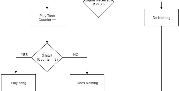
This code is used to track the number of hits on the 3DoT Rover when testing with the analog pin. It consists of a loop that is activated once the voltage on the receiver reaches 3.5v, and counts the number of times it reaches this level or higher. Below I present the pseudo code and the flow chart in hopes of better explaining this code.

4


Flowchart:

5


Once the micro-controller detects 3 hits, it will play a short song and then reset, and start over again.

Sources:

https://www.arduino.cc/en/Tutorial/ReadAnalogVoltage


Spring 2016 3DOT Goliath, Making Laser Tag Possible: The emitter

By: Kevin Moran (Electronics and Control Engineer)

In this post I will be discussing the IR emitter that is being used to make this game possible, and the components that go along with it:


Components:

IR LED: NTE30047

Transistor: 2N2222

Resistors: 8.6k and 110 ohm


The NPN transistor acts like a current regulator to ensure the IR LED is provided just enough current. The base which is connected to the 8.8k ohm resistor is connected to a digital pin on our micro-controller (3DoT or Arduino Nano) and this allows us to control when the emitter is on or off. The 110 ohm resistor is connected between the 5V supply and the positive side of the IR LED, while the ground is then connected to the collector.

1


This is the resistor value that allows us to use this NPN transistor as an on/off switch.


Fritzing Diagram:


2


Eagle CAD schematic:


3


Sources:

Jeffrey Cool: Division Manager

https://learn.sparkfun.com/tutorials/transistors


Spring 2016 3DOT Goliath, PCB Layout

By: Jerry Lui ( Manufacturing Engineer)

The general layout of the PCB was determined by the how sensitive the signal was, the specific wiring of IC’s to surface mounted components, and mounted surface area. Power input was placed away from sensitive signals and had a trace width of 32mm @ 1oz/ft^2 copper thickness (determined by the PCB house/fabricator) with a total temperature shift of 10C which allows total current of 1A. The trace thicknesses can be quickly determined by the following chart:

1


While laying out the board make sure to perform a DRC error check frequently. The included .DRU error checking file has generic limitations which may or may not adequately represent your fabrication houses’ design requirements (EagleCAD will always flag drill and VIA holes). The fabrication house will generally supply a .DRU file that can be used in place and will often allow traces to be placed closer together.

1


All of the signals were moved as far from the power input as possible in this case I have placed on the top left corner. The large power supply capacitor was also placed as close as possible to the power input and the rest of the circuit was laid out to take power from that capacitor. Also, components were placed similarly to how they were wired in the schematic as much as possible so that they are generally easier to follow and understand.


Note that there are red dotted lines (and blue underneath) along the perimeter that represent the ground polygon which is needed to create the ground plane (red for top layer, blue for bottom layer). The isolation width (free space between the traces and ground plane) was set to 12mils by default but was changed to 16mils as a precaution. This value is mainly determined by the fabrication house limits.


5


To place a trace on the other side of the board while you’re currently laying a trace (top to bottom) click on the middle mouse button. This will automatically create a VIA (electrically connected through hole) that connects both traces.


TIP: If you don’t create a ground plane first you can right-click on any GND signal and hide it. This will reduce the air-wires shown so that laying out the PCB will be easier. All GND signals will be hidden with this option but can be restored by typing “ratsnest *” in the command line.


TIP: Component values can be hidden by disabling the tValues layer. This makes it significantly less cluttered.

6


In the picture below, the ground plane has been created by hitting the “ratsnest” command. Pay close attention to capacitors during the ground plane creation. The “relief” option should be enabled so that the negative terminal can actually be soldered easily; this option is set on by default.


7

The mounting holes seen above were created using VIA’s. The size is determined by what screw or mounting system that’s planned on being used. In this case the size was set to 86.6mils or the standard inner drill size of a M2 screw.


Text such as the label “Goliath spr’16” can be placed using the “text tool” and should be placed on the tPlace or bPlace plane. Make sure to properly label components and the positive terminal, negative/ground terminal or both.


8


This is what the board will look like after being fabricated from OshPark.

9

Conclusion

Laying out a PCB can be time consuming depending on the amount of components on your board. Never use auto routing as the algorithm used is not that great. Remember to account for trace thicknesses, pin locations, and temperature limits for components.


Spring 2016 3DOT Goliath, Making Laser Tag Possible: The Receiver

By: Kevin Moran (Electronics and Control Engineer)


In this post I will be discussing my initial selection for the IR receiver and how I began testing its analog output.


Components:


Transistor: SFH 310 (Opto Semiconductor)

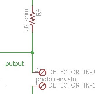
Resistor: 2M ohm

IR light


The phototransistor is a two legged transistor, with its third input being the output of the IR LED (Infrared Light).

  • When a light is shined, the electrons begin to diffuse from the emitter to the collector, this causes a voltage drop from its original 5V.
  • Unfortunately this signal is noisy and trying to use it directly for a game of laser tag would be very difficult. I present below the analog output of this transistor.


Arduino Plotter Graph:


1


Arduino Monitoring:

2

As can be appreciated from both the plotter and the monitor plots of the Arduino software, this analog signal is all over the place, the voltage drops varies depending on the distance of the LED from the receiver, and the length of time the light actually hits the receiver. Playing a game of laser tag with these results would not be very appropriate. The noise levels when no IR light is hitting the receiver are also shown on the Arduino plotter graph.

Note: The resistor value of 2M was chosen based on testing the sensitivity of the receiver with various values. 2 mega ohms turned out to be the best result


The code:

To read the analog voltage output

3


Eagle Cad Schematic:

4


Sources:

Jeff Cool: Division Manager

https://www.arduino.cc/

https://learn.sparkfun.com/tutorials/transistors

Spring 2016 3DOT Goliath, Making Laser Tag Possible: The Schmitt Trigger

By: Kevin Moran (Electronics and Control Engineer)

Since the analog output of the receiver is very noisy, my division manager suggested I use a Schmitt trigger which has 2 jobs:


  1. It reduces noise from the circuit through hysteresis, the time-based dependence of a system’s output on present and past inputs.
  2. It inverts the signal from the detector circuit and creates two thresholds-high and low. By changing resistor values we are able to control the high and low thresholds.

Below is the graph of a generic output using the Schmitt Trigger, as can be seen the signal is inverted, and the noise is relatively gone.


post


Now the challenge was selecting the correct Schmitt trigger that would work best with our receiver, after testing various resistor values, I made my choice between two sets of resistors.

2

I decided to go with the resistor values from Trigger 1, because It has a larger gap between the high and the low thresholds. When tested with the Phototransistor it provides a low threshold closer to 0 voltage

All values were taken with multi meter while changing the input voltage

Note: The high and low threshold change when the Resistor value connecting the receiver is changed from 100k ohms to 2M ohms (I did this in order to increase the sensitivity of the receiver)


Testing with Arduino Monitor:

  • When light is applied to the photo-transistor and the input is placed through the Schmitt trigger
    • High Voltage= 3.76 V
    • Low Voltage= 0.02 V

In order to make the phototransistor sensitive enough to be able to detect the IR light, I am using a 2 mega ohm resistor from the detector to the 5v supply

Both the high and low voltage thresholds are shown using the Serial Monitor

This is the result.

3

I also conducted a test on the Schmitt Trigger using a potentiometer

Components for this test:

10k potentiometer

LM358 Op-Amp

Resistors: 100k, 51k, 51k

Capacitors:  10 microF

Arduino Uno

The threshold between a high or low input from this test is 2.6V

As I varied the resistance in the potentiometer I obtained the graph provided in this slide

Based on this experiment I concluded that my Schmitt trigger was ready to be used alongside the photo-transistor.

4


Below is the result from this test using both the Arduino plotter and monitor

5


As can be seen again, a very clean signal that has only two outputs a low 0.02v and a high at 3.78v


Sources:


Jeffrey Cool: Division Manager

http://www.ti.com/lit/an/scea046/scea046.pdf

http://pcbheaven.com/wikipages/The_Schmitt_Trigger/

Spring 2016 3DOT Goliath,Assembling and Testing the 3Dot Board

By:  Ayman Aljohani (Project Manager)

For our Goliath project we will be using a custom made PCB that contains a microcontroller (known as the 3Dot Board) that will perform various tasks (ex. movement, laser shot, detector).  The physical PCB will be provided for us; however, it is required to solder all the components onto the PCB.

The steps we will be taking to solder the parts onto the PCB:

  1. Apply flux to the area you will be soldering and apply the soldering iron.
  2. Place the component on top of the soldering iron and heat the area to create contact between the soldered iron and the component.Soldering 3DOT Board components manually with Soldering Iron
  3. Check with multi-meter to make sure the components are connected to the PCB
  4. If alignment needs to fixed, we will use the heat gun to simultaneously heat the area to remove the component.
  5. Hold heat gun 3~4 inches away from the PCB for 30 seconds to heat up the board (prevent heat sync).                                                          heat gun
  6. Now aim the heat gun around 2 inches at the area you’re interested in for 15 seconds.Soldering with heat gun
  7. Apply little pressure to fix the alignment of the component.


Applying solder base to the area, this could be done in two ways:

a-All at once using stencil

Applying solder base using stencil

then clean the extra solder base manually

aplpling solder base


b-Manually apply solder base to all parts. This option takes loner time, but it will give a clear idea about 3DOT components and connections which makes the troubleshooting easier.


rsz_manually_solder_base


2- Use tweezers to place the components on the 3DOT Board:

rsz_tweezer  rsz_tweezer_2


3- After placing the component correctly, apply heat by placing the PCB in an oven


Assembled 3DOT Board:

rsz_final_product


The steps we will be taking to remove parts on the PCB:

  1. Apply flux to the area interested in to remove the soldering iron from a component.
  2. Put de-soldering on the area you want to absorb the soldering iron and apply the heated solder tip on top of it.
  3. Apply until you see the solder iron gets absorbed by the de-soldering material.
  4. Remove the component after most of the soldering iron has been removed.