PCB Layout Design and Guidelines
/in E&C - PCB Layout and Assembly/by arxterraA comprehensive guide to PCB Layout Design in Eagle CAD, covering everything from software use, design practices, and Fab Houses.
How to Make a Shield in Eagle CAD
/in E&C - PCB Layout and Assembly/by arxterraTable of Contents
Introduction
So you want to design a shield for your 3DoT board. First, which shield do you want to design? The 3DoT boards includes both a top “3DoT Shield” and front facing “Sensor Shield.” The 3DoT Shield is typically used to add functionality to the board; for example an accelerometer, gyro, Inertial Measurement Unit (IMU), compass, boost converter, or current monitor etc.. The sensor shield is typically used to add a downward facing sensor; for example an IR sensor, RGB color sensor, or CCD camera. This post shows you How to Design the 3DoT Shield.
The 3DoT Shield plugs into a 16 pin header and typically communicates with the Micro-controller Unit (MCU) via a serial communication protocol. The shield supports I2C, USART, and SPI serial interfaces.
In most cases the pins may also be used to implement a simple digital interface. It also can output a PWM (AnalogWrite) waveform or read an analog input (AnalogRead).
| Pin | Serial Pin | Digital Pin Name | Note |
|---|---|---|---|
| 2 | SCL | D3 | PWM Output |
| 3 | SDA | D2 | |
| 4 | RX | D0 | |
| 5 | TX | D1 | |
| 16 | MISO | D14 | |
| 15 | MOSI | D16 | |
| 14 | SCK | D15 | |
| 13 | SS | D17 | RXLED |
| 11 | A4 | A4 | May be used as digital pin |
In the following tutorial, I will show you how to design and layout a basic 3DoT Boost Shield by starting from an existing open source design.
Setup
This tutorial assumes you have a basic working knowledge of Eagle CAD. If you are new to Eagle CAD you may want to start by reading the blog posts on the Getting Started/Electronics and Control Resources page in the “PCB Design” Section. Before you begin, make sure your computer is configured with the latest software.
- Download and install Eagle CAD
- Download and place in Eagle CAD dru folder OshPark Design Rules
3DoT Boost Shield Tutorial
So what functionality do you want to add to your robot? To travel in a straight line or turn you may want to add a gyro, compass, and/or rotary (also known as a shaft) encoders. To run 5 or 6 volt motors or servos consider adding a boost converter. If you do add a boost converter, you will want to make sure you do not exceed the 1.3 A capability of the CR123A Li-Ion battery by including a current sensor. Technical Note: The current limit of the 3DoT Power Management IC (PMIC) chip is set to 1.0 A.
In many instances, you can download Eagle CAD layouts and simply adjust the form factor and pin assignments to make your 3DoT shield. Eagle CAD designs are provided by the Arduino Community, Digi-Key Designer, and SparkFun.
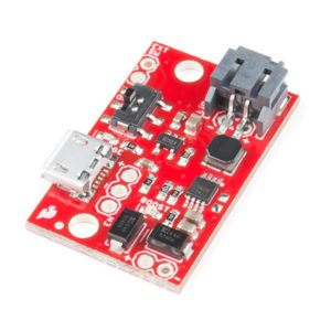
For my tutorial, I am going to make a 5v boost converter based on the SparkFun LiPo Charger/Booster – 5V/1A.
So lets begin.
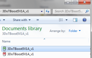
Step 1 – Download: Download the Eagle Files found here. Make a copy of the folder and rename the board (.brd), and schematic (.sch) files and the folder 3DoTBoost5V1A_v1. As you work on your design remember to save often.
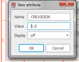
Step 2 – Replace the Frame: Open your soon to be new 3DoT shield in Eagle CAD. Delete the SparkFun Frame and replace it with the FRAME-A4L device found in the SparkFun-Aesthetic Library. Follow these instructions to set the CNAME, DESIGNER, and CREVISION values in the title block:
- Right click the origin of the title FRAME (Small red cross seen near the bottom-left of Figure 4) and select Attributes from the pop-up menu.
- Click the New button.
- Enter the name you want to change, in the example “CREVISION”
- Enter the value you want displayed, in the example “1.0”
Step 3 – Simplify the Schematic: The 3DoT board includes a Li-Ion Battery charger so we can delete the top half LiPo Charger Booster of the schematic leaving the Switching Regulator Circuit. We are going to be switching from the SparkFun breakout board connectors to our 3DoT headers so you can delete Jumpers J5, and J6.
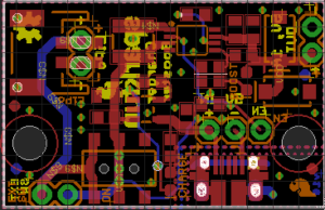
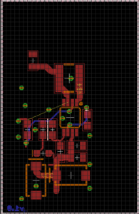
Step 4 – Simplify the Board Layout: Now lets cleanup the original Sparkfun Charger/Booster layout shown in Figure r5 by removing artwork, vias, and traces that are now longer applicable.
- Show Layers 21 tPlace and 22 bPlace ONLY (verify layers 39 tKeepout and 40 bKeepout are Hidden). Block select everything and delete. Don’t worry, artwork that is associated with components will not be deleted. Show the layers you just hid. The board should now look like Figure 6 “Boost Only.”
- Rename v10 on bottom layer v1.0.
- Remove unused “shield” polygon.
- Restore Top and Bottom GND polygons to rectangles with dimensions equivalent to the board.
- Remove ground traces and vias that are outside the boost circuit. If they are not already visible show layers 23 tOrigins and 24 bOrigins.
- Block select Boost Circuit and move closer to the left of the board.
Your board should now look similar to Figure 7.
Congratulations, your design is now ready to be configured as a 3DoT Shield.
Step 5 – Add 3DoT Shield:
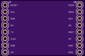
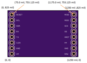
The 3DoT Shield with dimensional information is shown in Figure 7. Follow these instructions, to place your boost circuit on the 3DoT Shield. Don’t panic if the circuit does not fit inside the 3DoT shield. We will be working on this problem after we wire up the connectors.
- Redefine your boost shield’s border plus top and bottom ground planes as defined in Figure 7.
- From the SparkFun-Connectors-8pin library add two (2) CONN_08>CONN_08″ devices. They should automatically be labeled J1 and J2.
- Place J1 (left) and J2 (right) in the orientation and location defined in Figure 8.
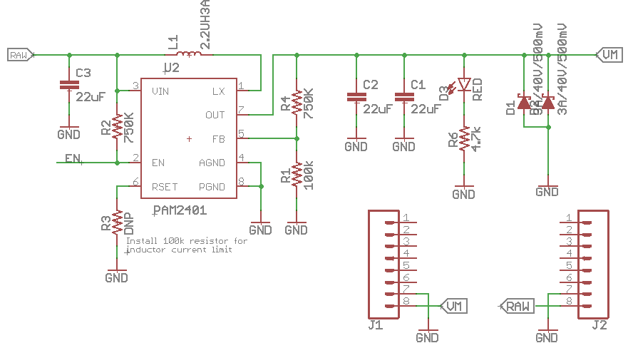
Step 6 – Wire Boost Circuit to 3DoT Shield Connectors: Open the schematic window. For our boost circuit we only need to wire the input J2 pin 8 RAW and output J1 pin 10 VM to our circuit. RAW is wired to our battery through a Power Management IC (PMIC) chip. The PMIC in turn is enabled by the switch on the 3DoT board. The VM pin is wired to the motor driver and servo power connectors.
- Add and Name traces VM, RAW, and two GND pins on J1 and J2 as shown in Figure 8 (bottom right). The attractive label symbols are enabled by checking the xref box in the symbols property window. Notice that relative to the J1 and J2 connectors, the input (RAW) is on the right and the output (VM) on the left.
- Returning to the boost schematic. Rename VBATT -> RAW and VCC -> VM. Add labels and clean-up the design. Notice that relative to the circuit, the input (RAW) is now on the left and the output (VM) is now on the right. My final circuit is shown in Figure 9.
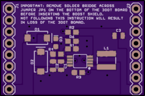
Step 7 – Complete the Board Layout: Switch to the board view window.
- You should now see the layout of the boost circuit connected to the J1 and J2 connectors by air wires (layer 19 Unrouted). With a little tilt of your head you hopefully can see that with a simple rotation to the right (clockwise) the circuit will line up quite nicely with connectors.
- Run 32 mil traces for VM and RAW. Because I am never happy with good enough, I used polygon fills for the VM and RAW traces. Do not forget to name the polygon. For my design I needed to also change the rank of the polygon fills to 1, and the top plane to 2.
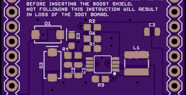
- Although the 3DoT Board is designed to support a Boost Shield, unless the solder bridge across Jumper 1 is removed, a short will occur when the boost shield is plugged in destroying the 3DoT board! To make sure the user is aware of this potential danger to the board, add a note on Layer 21 tPlace with the following text “IMPORTANT: REMOVE SOLDER BRIDGE ACROSS JUMPER J1 ON THE BOTTOM OF THE 3DOT BOARD BEFORE INSERTING THE BOOST SHIELD. NOT FOLLOWING THIS INSTRUCTION WILL RESULT IN LOSS OF THE 3DOT BOARD.“
- Congratulations you have just made your first 3DoT shield!
On your Own
While my design is good it could be better. Here are two modifications you can make to improve your boost shield.
- Assign one of the unused serial interface pins as a digital pin and wire to the EN trace. Now you can turn the boost circuit on and off through software. This is especially important if you want to avoid a large an inrush of current when the 3DoT board is initially turned on and to save power when the motors are off.
- Add a current sensing circuit to your shield. Whenever you run motors and servos, especially with a boost circuit, it is important to manage the amount of current drawn by the robot. For example, to turn off the motors if one of them stalls resulting in excessive current being drawn which will result in the loss of the motor and potentially the 3DoT board as well.
Soldering Workshop
/in E&C - PCB Layout and Assembly/by Jordan SmallwoodBy: Diane Kim (Division Manager for E&C)
Verified By: Jordan Smallwood (Project Manager)
Approved By: Miguel Garcia (Quality Assurance)
Table of Contents
Introduction
The Soldering workshop was focused on hand soldering. Based on the PCB designs of each project, the components that were to be hand soldered were the through-hole components, more specifically the connectors and the IR LEDs. Since we had access to a soldering iron, we practiced soldering based on the guide from Adafruit to understand how to solder. I have access to a PCB fabricating machine called the Othermill from Batam tools and printed out practice circuits for the group to practice on as well as provide connectors if needed.
Guide To Soldering
Required Tools
- Solder Iron
- Wet Sponge/Brass Mess
- Solder
- Wires
- Through-Hole Components
- Solder Sucker/Wick
First Step: Check Tools/Materials
Before you turn on the soldering iron, make sure to check whether the tip is clean or not. If the tip is not clean (when it is oxidized) it can prevent the tip of the soldering iron from heating up properly. To make sure that this doesn’t happen, we need to always make sure to clean the tip using the wet sponge and brass mesh and thin the tip after each use so the tip acts as a protective layer.
The type of solder also determines what temperature to set the iron on. If the solder is lead-based the temperature of the iron should be set to around 650 degrees Fahrenheit, and if the solder is lead-free it is best to set the temperature around 750 degrees Fahrenheit. The temperature setting is important to properly heat up the conductive pads and the wires or through-hole components.
Soldering
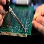
When the soldering iron reaches the desired temperature, the iron is placed in the joint of the pad and the component wire lead. The solder should first touch the iron and then to the wire lead and the pad for a secure connection. Then remove the iron and solder for it to cool. It is also important to make sure that the heat is not applied for too long to prevent overheating. A good solder is when the solder covers the whole pad and the wire lead and it has a slanted slope connecting the wire lead and the pad. It also looks smooth and shiny on the surface. If the solder is dark and is in a ball like shape that means that not enough heat or uneven heat was applied to the pads which are called the cold joint.
Making Mistakes:
Sometimes when the pads are so close, it can be shorted during the soldering process. To remove the excess solder, you can use a solder sucker or solder wick to remove the solder. The solder sucker sucks the solder out and the solder wick soaks up the excess solder.
Soldering Workshop:
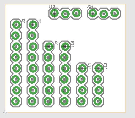
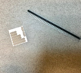
The groups first went over the basics of soldering and then I provided practice boards so that they could practice. The practice board consisted of connectors that varied in the number of pinheads (8, 6, 4, 3). Female connectors were also provided to practice soldering.
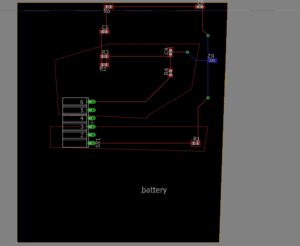
Figure 1: Eagle Board file of the practice board for soldering
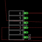
The practice board consists of 2 of each 8, 6, 4, and 3 pinhead connectors.
Figure 2: Photo of the practice board after printing and female connectors that are provided
Conclusion:
The group knew how to solder prior to the workshop but were able to practice to avoid making mistakes that would cost them the whole board. Since they were able to practice soldering on connectors which is what they will be soldering on for their PCB, it was more applicable to their projects.
When it comes to surface mount soldering, I went over the theory of how to apply the solder paste and how to bake the board; however, since I have access to a PCB fabrication machine that can print the solder paste and bake the board, we will be using that for the PCBs for our projects. The PCB fabrication machine that we are using is the V-one from Voltera.
References:
The information about soldering is based off a tutorial on Adafruit:
Fritzing Diagram Training
/in E&C - PCB Layout and Assembly/by Jordan SmallwoodBy: Diane Kim (Division Manager of E&C Hardware)
Verified By: Jordan Smallwood (Pathfinder Project Manager)
Approved by: Miguel Garcia (Quality Assurance)
Table of Contents
Introduction
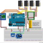
Fritzing is a program that allows easy PCB design. It allows the user to convert their design on breadboard to CAD files. On the breadboard view, there are parts that are commonly used such as Arduino boards, resistors, motor drivers, and Bluetooth modules. The breadboard view can also be converted into the schematic.
Training
We spent one week on the training for the Fritzing program. We used the documentation from the EE400D website. One document focused more on the steps to use the program. It started from the working on the breadboard view. The documentation worked on creating a fritzing diagram for a motor driver and Bluetooth. Since I was new to the program as well as the division manager, I went over through the program first and created the diagram. I provided the documentation and walked through the process with the group. The assignment was graded as a homework.
Key Points
- Make sure the wires and the connections are visible, curve the wires in order to do so.
- If the exact components are available, the packages may be there, so it can be used as a replacement.
- If no replacement, you can make your own components which are shown in the second document
Conclusion
The use of the Fritzing diagram for this class was mainly focused on presenting. It was used for showing what type of components and the connections between them and the microcontroller. The one thing that we could have worked on is making custom components within the Fritzing diagram, but we didn’t go over that because none of the teams needed to make custom components.
References
Eagle CAD Training
/in E&C - PCB Layout and Assembly/by Jordan SmallwoodBy: Diane Kim (Division Manager of E&C Hardware)
Verified By: Jordan Smallwood (Pathfinder Project Manager)
Approved By: Miguel Garcia (Quality Assurance)
Table of Contents
Introduction
Eagle is a program used to design and layout custom boards. We went through a series of training for using Eagle CAD.
Training 1: Schematic
The first training was based off the documentation from Sparkfun. It was focused on designing the schematic. These were the points of the program that we went over:
- Adding the components
- Package, type, and SMD or Through-Hole
- Moving and rotating the components
- Connecting the components use the “NET” function
- Deleting and copying the components
- Labeling and naming the components and the values
- Adding new libraries
- Using the ERC command
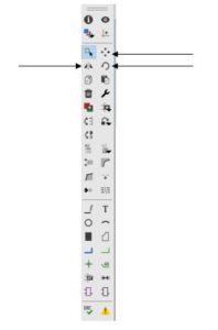
Figure 1: Toolbar of the Eagle Schematic
Training 2: Board
The second training was focused on designing the board layout. These are the key points that were went over.
- Layers: Top and bottom
- Routing the layers
- Auto-routing
- Placing the components
- Talk about Female and Male header connections
- Possible restrictions (Size, placements, drill size and trace size)
- DRC command
- Copper pours for GND and PWR
- Effective GND and PWR connection
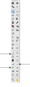
Figure 2: Toolbar for Eagle Board
Training 3: Practice
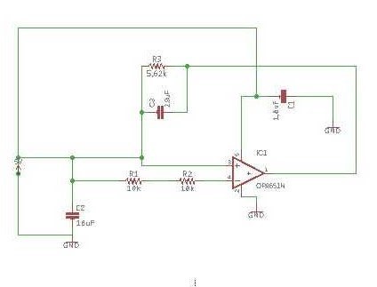
This training was focused on applying what was learned. The first practice was done together where a simple low filter schematic was given to design on Eagle.
Figure 3: Low Pass Filter Schematic using Operational Amplifier
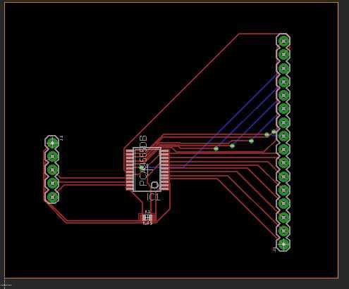
After the first practice, the second assignments were given as homework. The second assignment given was to design an I/O expander circuit.
Figure 4: Board Design of I/O Expander HW assignment
Training 4: Quiz
For the last part of the application, I assigned two quizzes. Each quiz was 40 minutes long and were given a simple circuit to design on the schematic and board. There were certain restrictions such as the mil size, the placement of the connectors, the size of the board, and the components’ packages. The grading criteria is the following:
- Did you follow the schematic?
- Did you follow the instructions? (such as package size)
- Is the position of the connectors appropriate?
- The overall quality
- Did you route everything?
- Did you ground the board or did you add the copper pours?
- Did you make it compact as possible? (Within the given size)
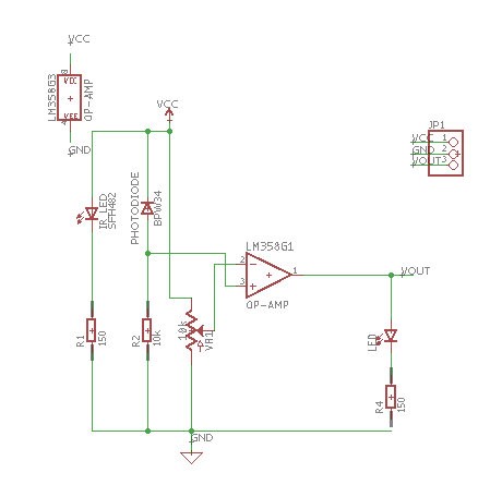
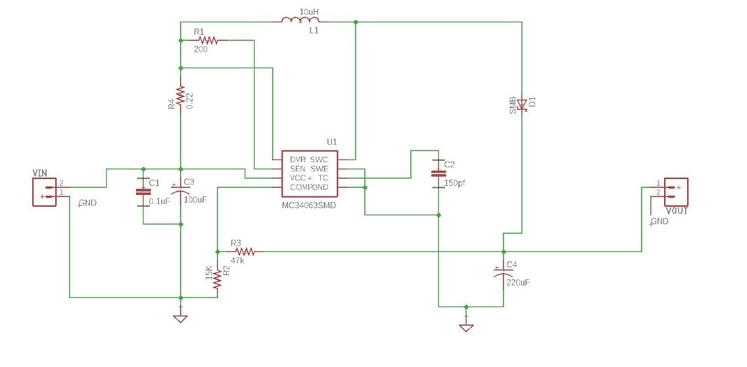
The first quiz was an IR sensor and the second is the boost converter. The schematics are shown below
Figure 5: Quiz 1, IR sensor
Figure 6: Quiz 2, Boost Converter
References
Eagle CAD Training
/in E&C - PCB Layout and Assembly, E&C Resources, Training/by Muhannad Al MohamedWritten By: Muhannad Al Mohamed (E&C DM)
Table of Contents
Objective
This blog is intended to introduce Eagle CAD designing application to members to be able to design schematics for electronic circuits. The members of the E&C division are required to know how to make schematics of customed printed circuit boards (PCB) for their corresponding projects. These schematics can be used to design the layout version of the PCB in the Eagle CAD layout part. The layout of the PCB can then be used to generate Gerber files; which can be sent to fabrication houses to make the PCBs.
Creating New Sketch
To start a new sketch a new project should be created and a name should be given to it. After that, a new schematic should be created within the project.
Adding Parts
To add a part from the EagleCAD library, the add icon should be clicked where the list of all the parts would show in a window.
Parts can be chosen directly from the libraries by double-clicking on each part. The search window can be used to easily find a specific part. However, the EagleCAD search engine is literal; which means that any misspelling in the part name will not show any result. To avoid that, stars should be typed before and after the part’s name.
Placing parts
Placing a part is simple, one click should input parts into the schematic and by clicking escape twice it would quit the adding mode. To rotate parts, right click before placing any part. Rotation of a part or a group of parts can be obtained by clicking the rotate icons.
Connecting Pins
To connect placed parts the net icon should be clicked. The edge of each pin should be clicked when connecting parts to ensure that you are connecting to the part not just drawing a line on it.
When connecting to a part make sure that a connecting window shows up asking for permission to connect to a part. When a connecting is done, double-clicking the crouser will quit the connecting mode.
When connecting a line with a line, make sure that a junction shows at the intersection. If there is no junction showing, a junction can be added by clicking the junction icon.
Labeling Pins and Parts
Parts can be given labels that can show names and values in both the schematic and PCB layout designs. To add a name label click on the name label and click on the desired part. A value label can be added to parts as well by clicking on the value label. Just a reminder, the value label is still just a name and does not have any relation to the part’s characteristics.
Pins can be named as well by giving them labels by clicking on the label icon and clicking on the desired pin.If a pin is named exactly with the same name to another pin, a window should pop up asking to connect the pins. If clicked true, the pins would be automatically connected without showing a line. The labels appearance can be changed by clicking on the tag icon and the size of the label can be changed as well.
EagleCAD Libraries
EagleCAD has a lot of different libraries from various retailers and manufacturers. It also has the regular parts such as supplies, passive components, .. etc. However, sometimes the desired part is not found in the EagleCAD built-in library so in that case a new library should be added.
Adding Libraries
To add a library, its “.lbr” file should be downloaded first from the manufacturers’ website or from different websites that provide eagle libraries:
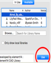
Once the “.lbr” file is downloaded it should be placed in the “lbr” folder in the application’s folders. After that, the library should be indicated as used in the library manager window.
Testing
Verify Connected Pins
If the pins were labeled with similar names, their connection can be checked by clicking the show icon. Once the show icon is clicked, by clicking on any pin it would show the connected pins the clicked pin in bold font. It is very helpful to trace pins and check if all the parts are connected correctly.
Checking Errors
After creating the schematic, the design should be checked if it has any errors. By clicking on the ERC icon a window should pop up showing any electrical errors. Make sure that you have no errors befor going to the PCD layout part of designing.
Training Material
Schematic Training
Further trainings on creating EagleCAD schematics can be found here:
PCB Layout Training
Training on the making of the layout version of the custom PCB can be found in this blog written by Charles Banuelos (MFG DM).
Eagle Cad Lecture series
/in E&C - PCB Layout and Assembly, E&C Resources, Training/by charles banuelosWritten by Charles Banuelos MFG DM
Table of Contents
Written 11/2/2017
The division has finished learning Eagle Cad. The first of the two tutorials covered moving of components in eagle cad along with switching to the PCB layout so that they may start to build. The second tutorial covered how to create traces and nets on the PCB. The lecture then covered what vias are and how to place them. The lecture followed with showing how that the use of both sides of the board which will make the designs of the PCB easier to come up with. The lecture then went into how to use polygons. The part of the lecture that teaches polygons might be the most important of the whole lecture. The polygon function allows for the creation of power planes and ground planes. These planes can be a small square in the corner of the board or it can take up the whole board. The lecture continues with how to do DRC checks. The lecture then goes over how to get the .dru files from OSH park in order to use their checks so that the boards can be built. The lecture concludes with making the Gerber files. The lecture shows how to download OSH parks gerber file presets. This allows for all of the Division members to turn in the correct files to make their PCB’s.
Update 11/30/2017
The lectures below along with the quiz and supplemental material provided will be able to teach students how to create PCBs given they are already given the schematics.
EagleCad Training Part 1
-To start a New Project you must first either create a new schematic or open a schematic. To start a new schematic you first open eagle and then click on file in the upper left hand corner. Then click on new and then schematic. You will then be able to start populating the schematic work space. To place parts you press on the add icon located on the left side of the work space.
This space is very extremely sensitive to both spelling as well as capitalization for parts.
To move the parts around the board you must press on the move button and then on the cross on each part to move the part. To rotate the components it is the same procedure but you must press the rotation button first.
To connect the part you use the line or net button. If you would like two lines to branch from a single point or come to a single point you must use the junction button in the lower left corner.
Once the schematic is deemed correct it is time to create the PCB. To open an already existing schematic go to file and then open. This allows you to open the correct file.
To create the PCB one must click on file and then on the button switch to board. To populate the board it is the same operation as the schematic. To move the parts click on the move tool and on the cross on the part. You will then be able to drag the part to the desired location.
EagleCad Training Part 2
Once the board has been populated you be able to start creating traces. To create traces on the PCB the route tool on the left side of the work space must be used. To use this tool click on the route tool and then on the place you would like the trace to start.
It is common practice to always use 45 degrees when designing PCBs. To view the angle of being drawn click on the route tool and then at top of the page you will see the different possible angles available. To finish a trace click on the point you wish to end the trace.
To place parts on the bottom layer of the board the person placing the parts will need a mouse or will need to click on the mirror button. To place parts on the bottom layer with a mouse the user will have to click on the move button and then on the part. Once the part has been clicked on the person will click on the mouse wheel which will make the part turn blue which means that the part is on the bottom of the board. The mirror button will also be able to do the same thing in the PCB work space.
To run a trace to this part a via will need to be placed. The first way to place a via is too manually place the via using the via tool located towards the middle of the tool bar.
The second way to place a via to first run a trace to a certain point. The person will then click to stop the route but will still be able to draw a route. The user will go to the upper corner of the of the work space and click on the select layer drop down which is located next to the grid button. The user will select bottom layer which will create a via to which the top layer route will already be connected to. The user will then be able to continue the route in blue on the bottom of the board.
To remove an unwanted route the user must click on the rip up tool located next to the route tool.
To view all of the layers of the board you can click on the layers setting in the upper left corner of the work space.
To create polygons it is key to remember that a polygon must start and end at the same point on the board. Polygons are useful in order to create power and ground planes for the whole board or specific portions of the board. Once created these can be moved or changed using the move tool. These polygons can be created on both the top and bottom layers using same layer selecting button. To name the polygon, the user must right click on the edge of the polygon and go to properties. The name of the polygon is case secretive and will be close to the bottom of the window. The naming of a polygon will allow for any part that is connected to that name to be automatically connected once the rat nest button on the bottom of the tool bar is collected. It is common practice to have either the whole top or bottom layer be power and the other layer be ground.
DRC checks are vital to completing a PCB layout. The DRC check used is the custom one made by Professor Hill. This DRC check is given below and should be the only one used because every fab house should be able to use this one. To use this DRC it will need to be downloaded and saved into the DRU files within the Eagle program. To perform a check click on the DRC check at the bottom of the tool bar. The user will then click on load and the correct DRC check. The user will then press the check button. This will generate an error report will have all of the errors of the PCB. The errors will need to be cleared for ordering of the board. It is also important to remember to turn on all layers before running the check.
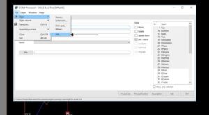
The last thing that is needed to create gerber files. To create gerber files you first go to the fab house that you plan on ordering from and seeing if they have the job files pre-made for you. OSH park already has these made for you and are easily downloadable. These job files once downloaded will need to be saved into eagle and specifically into the cam folder. Once the job has been saved it is time to generate the files. To generate the files go to file and then cam processor. Then go to file in the cam processor window and then open and then job. Click on the correct job and then make sure the files are being saved into the right area. To conclude the making of the Gerber files click on process job. If the cam files are unavailable from the fab house you wish to use then the cam files must be created in accordance with fabrication houses rules. To create these jobs one must click on the layer needed along with the names and file type. This concludes with pressing add and must be done for each layer.
Extra Training Material Provided by Eagle on YouTube
