Laying out things to keep in mind when formulating particular blog posts.
By: Diane Kim (Division Manager for E&C)
Verified By: Jordan Smallwood (Project Manager)
Approved By: Miguel Garcia (Quality Assurance)
Table of Contents
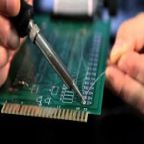
The Soldering workshop was focused on hand soldering. Based on the PCB designs of each project, the components that were to be hand soldered were the through-hole components, more specifically the connectors and the IR LEDs. Since we had access to a soldering iron, we practiced soldering based on the guide from Adafruit to understand how to solder. I have access to a PCB fabricating machine called the Othermill from Batam tools and printed out practice circuits for the group to practice on as well as provide connectors if needed.
Before you turn on the soldering iron, make sure to check whether the tip is clean or not. If the tip is not clean (when it is oxidized) it can prevent the tip of the soldering iron from heating up properly. To make sure that this doesn’t happen, we need to always make sure to clean the tip using the wet sponge and brass mesh and thin the tip after each use so the tip acts as a protective layer.
The type of solder also determines what temperature to set the iron on. If the solder is lead-based the temperature of the iron should be set to around 650 degrees Fahrenheit, and if the solder is lead-free it is best to set the temperature around 750 degrees Fahrenheit. The temperature setting is important to properly heat up the conductive pads and the wires or through-hole components.
When the soldering iron reaches the desired temperature, the iron is placed in the joint of the pad and the component wire lead. The solder should first touch the iron and then to the wire lead and the pad for a secure connection. Then remove the iron and solder for it to cool. It is also important to make sure that the heat is not applied for too long to prevent overheating. A good solder is when the solder covers the whole pad and the wire lead and it has a slanted slope connecting the wire lead and the pad. It also looks smooth and shiny on the surface. If the solder is dark and is in a ball like shape that means that not enough heat or uneven heat was applied to the pads which are called the cold joint.
Sometimes when the pads are so close, it can be shorted during the soldering process. To remove the excess solder, you can use a solder sucker or solder wick to remove the solder. The solder sucker sucks the solder out and the solder wick soaks up the excess solder.
The groups first went over the basics of soldering and then I provided practice boards so that they could practice. The practice board consisted of connectors that varied in the number of pinheads (8, 6, 4, 3). Female connectors were also provided to practice soldering.
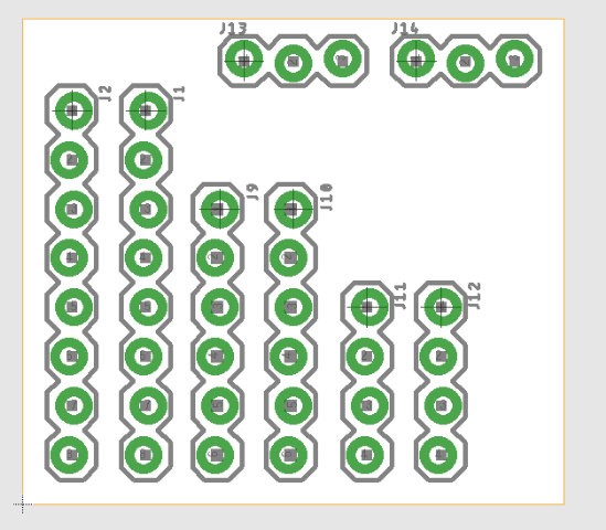
Figure 1: Eagle Board file of the practice board for soldering
The practice board consists of 2 of each 8, 6, 4, and 3 pinhead connectors.
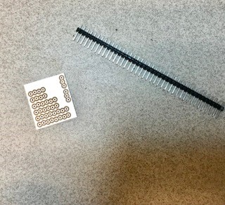
Figure 2: Photo of the practice board after printing and female connectors that are provided
The group knew how to solder prior to the workshop but were able to practice to avoid making mistakes that would cost them the whole board. Since they were able to practice soldering on connectors which is what they will be soldering on for their PCB, it was more applicable to their projects.
When it comes to surface mount soldering, I went over the theory of how to apply the solder paste and how to bake the board; however, since I have access to a PCB fabrication machine that can print the solder paste and bake the board, we will be using that for the PCBs for our projects. The PCB fabrication machine that we are using is the V-one from Voltera.
The information about soldering is based off a tutorial on Adafruit:
By: Joseph Cho (Mission, Systems, and Testing)
Verified By: Intiser Kabir (Project Manager)
Approved By: Miguel Garcia (Quality Assurance)
Table of Contents
The interface matrix will be used by the MST engineer and the E&C Hardware engineer to allocate the pinouts of the main PCB. The main PCB should be where the central processing is done. The 3DoT Board is the main PCB containing the microcontroller (ATmega32u4). If you have all the components picked out for the robot, the interface process should be easy.
In order to start interfacing, we need to know what parts are used in the robot and how those parts are connected. A system block diagram will be very helpful to keep you organized.
If I2C addressing will be used, look up the I2C address of those parts (link to Adafruit I2C Address). I2C addresses have to be looked up to make sure that the parts that are being used do not overlap with other parts of the I2C bus. If addresses are overlapped, it is like having two people talking back to you the same time. Avoid having I2C addresses overlapped. We can use an I2C expander to avoid overlapping I2C addresses. While you are making a list of components, find a datasheet for each one of them. The datasheet will be used to pinout the PCB shields.

Figure 1: Interface Matrix Template
Description:
The 3DoT board has 16 available pins (2×8 pin) on the top of the board and 8 pins on the front of the board. You will start the interfacing by deciding how many pins will be utilized by the 3DoT Board. The interface matrix will be focusing on the leftmost column. Column B shows the pin names on top of the board, and Column C shows pin names on the front of the board. For the parts’ pin names, use the given pin name in the datasheet or schematic.
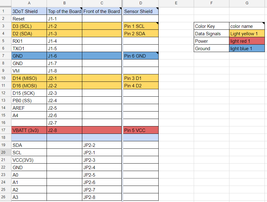
Figure 2: Example of 3DoT Interfacing (included in the Template)
Description:
In this example, 6 pins have been utilized for the sensor shield. I have named and numbered those pins for easier reference in the future. The color codes can be decided on your own, but for this example, I have used yellow, red and blue. I have separated them this way because those pins have different uses. The color yellow is used for the data signals, red is for power, and blue is for ground.
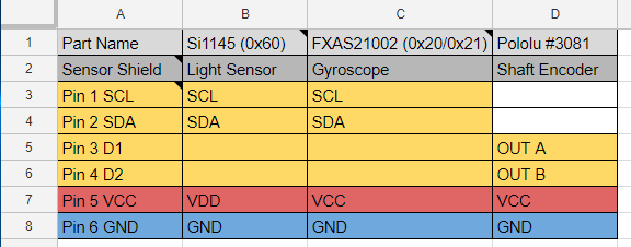
Figure 3: Example of PCB Interfacing
Description:
Now that we have those 6 pins ready for use, connect them to the parts to the correct pins. As mentioned before, some parts may share the I2C pins (SCL and SDA) and this is totally fine unless their I2C addresses overlap. If that is the case, use an I2C expander to re-address the parts’ I2C addresses. The “Shaft Encoder” has two separate pins for the digital output, so they are connected to two separate digital pins on the shield. Note that the row is colored up to the column used. Since shaft encoder does not use pin 1 SCL and pin 2 SDA, they are not colored in.
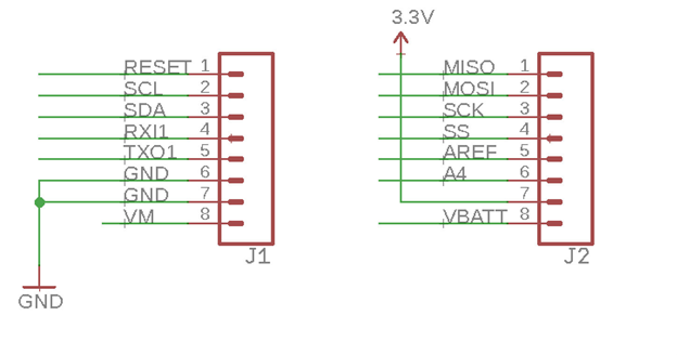
Figure 4: Pin of 3DoT board (Front of the board)
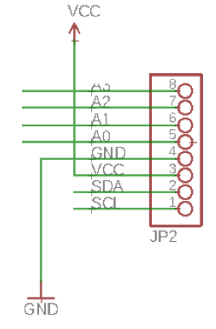
Figure 5: Pins of the 3DoT board (Front of the Board)
Description:
Schematics of the 3DoT board headers were added for reference. Look at the Arxterra website for more information about the 3DoT board.
Once the proper research is done for interfacing, the interface matrix is very simple to make. Read the notes in the examples and on the template for some parts skipped in this blog post. Lastly, double check your connections and get the matrix approved.