Advanced Arduino Assembly – Class Lectures
Introduction to AVR Assembly Language Programming
READING
The AVR Microcontroller and Embedded Systems using Assembly and C by Muhammad Ali Mazidi, Sarmad Naimi, and Sepehr Naimi
Sections: 0.1, 0.2, 1.1, 2.5, 2.6, 2.7
SOURCE MATERIAL
These are some of the sources I used to develop the material used in the lecture series.
- Reduced Instruction Set Computer
- Atmel AVR Assembler User Guide
- Atmel AVR
- AVR Quick Reference Guide:
- ATmega328P Summary (26 pages)
- ATmega328P (448 pages)
- 8-bit AVR Instruction Set (155 pages)
Table of Contents
What is an Embedded System?
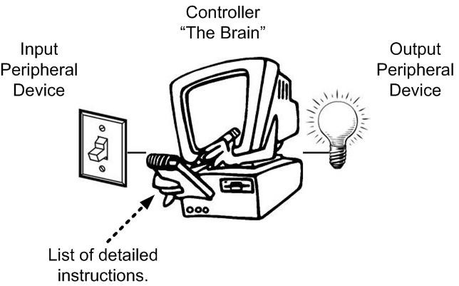
- An embedded system is an electronic system that contains at least one controlling device, i.e. “the brain”, but in such a way that it is hidden from the end user. That is, the controller is embedded so far in the system that usually users don’t realize its presence.
- Embedded systems perform a dedicated function.
What is the Controlling Device?
| EE Course | Technology | Tools |
| EE201 | Discrete Logic | Boolean Algebra |
| EE301 | Field Programmable Gate Array (FPGA), Application-Specific Integrated Circuit (ASIC) | HDL (typically VHDL or Verilog) |
| EE346 | Microcontroller | Program (typically C++ or Assembly) |
| EE443 | System on a Chip (SoC) | System Level Design Language |
What is an Arduino?
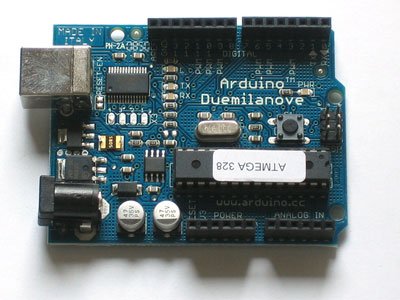
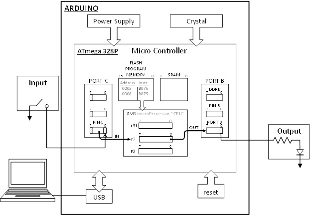
- Arduino is an open-source electronics PCB containing a microcontroller and the things needed to support it: Power Supply, Communications, Reset Button, Clock, and Connectors for adding Sensors and Actuators in the physical world.
-
Using an Arduino you can develop interactive objects, taking inputs from a variety of switches or sensors, and controlling a variety of lights, motors, and other physical outputs.
- The Arduino consists of two parts; the hardware and the software.
- We will be using the Arduino Uno which contains an ATmega328P 8 bit microcontroller.
- We will be using AVR Studio to develop the software for the Arduino in place of the Arduino IDE and associated Scripting Language.
What is a CSULB Shield?
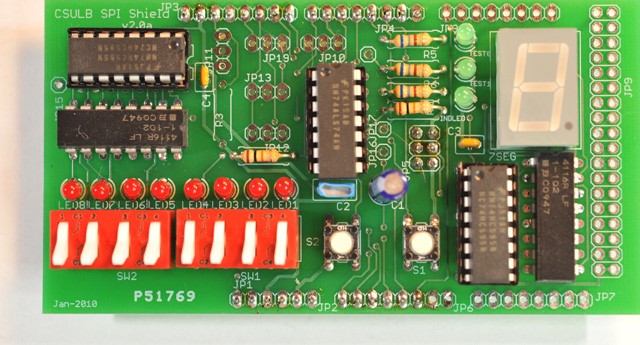
The CSULB Shield was designed to meet the educational objectives of EE 346.
The shield works with the Arduino Uno, Duemilanove (rev 2009b), and Mega Microcontroller Boards.
CSULB Shield Specifications
- Input
- 8 Toggle Switches
- General Purpose Push Button
- Reset Button
- Output
- 8 Discrete Red LEDs
- 3 Discrete Green LEDs
- 1 7-Segment Display
Building Blocks
What is an Input and Output Peripheral Device?
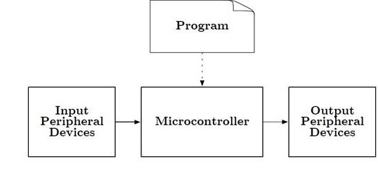
- A device attached to a controlling mechanism, for example a computer, yet is not actually part of the controlling mechanism, and whose operation is functionally dependent upon the controlling mechanism.
How do you design this controlling mechanism?
- If you control peripherals using Discrete Electronics or a Programmable Logic Device (PLD) such as an FPGA or ASIC, then the control is in hardware (EE201, EE301).
- If you control peripherals using a Microcontroller then the control is in software (EE346 and EE444), implemented by a Program.
- If you control peripheral using a System on a Chip (SoC) then the control may be in software and/or hardware (EE443).
What is a Program?
- The Program is a “very specific list of instructions” to the computer.
- The process of “creating the program” is where much of an electrical engineer’s time is spent.
- The program is often referred to as Software, while the physical system components are called Hardware. Software held within non-volatile memory is called Firmware.
- Software design is all about creating patterns of 0’s and 1’s in order to get the computer to do what we want. These 0’s and 1’s are known as Machine Code.
0010 0111 0000 0000 → 1110 1111 0001 1111 → 1011 1001 0000 0111 → 1011 1001 0001 1000
1011 1001 0000 0100 → 1011 0000 0111 0110 → 1011 1000 0111 0101 → 1100 1111 1111 1101
- The architecture of the processer (or computer) within a microcontroller is unique as are the Machine Code Instructions it understands.
0010 0111 0000 0000
1110 1111 0001 1111
- The list of Machine Code Instructions understood by a Microcontroller is known as the Machine Language.
How is Machine Code Related to Assembly Language?
Machine Code (The language of the machine)
- Binary Code (bit sequence) that directs the computer to carry out (execute) a pre-defined operation.
0010 0111 0000 0000
1110 1111 0001 1111
1011 1001 0000 0111
1011 1001 0001 1000
Assembly Language
- A computer language where there is a one-to-one correspondence between a symbolic (assembly language instruction) and a machine code
- The language of the machine in human readable form
clr r16
ser r17
out DDRC, r16
out PORTC, r17
Corollary
- Specific to a single computer or class of computers (non-portable)
Anatomy of an Assembly Instruction?
Sample Code Segment
| Machine Code | Assembly Code | |
| Binary | Hex | |
| 0010 0111 0000 0000 | 0x2700 | clr r16 |
| 1110 1111 0001 1111 | 0xEF1F | ser r17 |
| 1011 1001 0000 0111 | 0xB907 | out DDRC, r16 |
| 1011 1001 0001 1000 | 0xB918 | out PORTC, r17 |
- The Operation Code or Opcode for short, is a mnemonic that tells the CPU what instruction is to be executed. In the sample code above that would be clr (clear), ser (set register), and out (output to I/O location). One or more operands follow the Opcode.
- The Operand(s) specify the location of the data that is to be operated on by the CPU. In many cases it is the Arithmetic Logic Unit (ALU) that performs the specified operation.
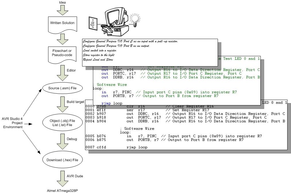
Design Example
Write an Assembly Program to turn a light on and off with a switch. A similar program was used in the design of The Wake-up Machine.
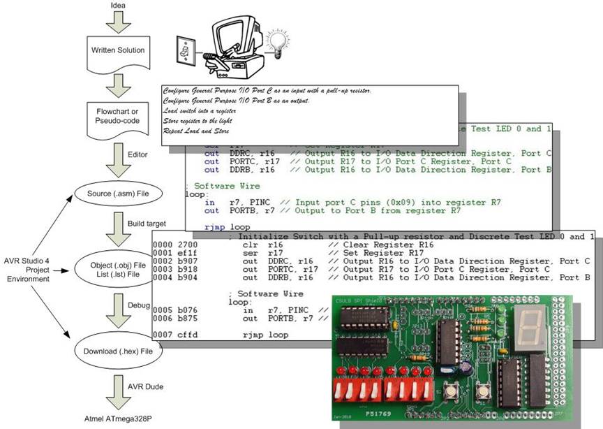
Development Steps
Assembly and Microcontroller Overview
Help
0010 0111 0000 00002 = 270016 = clr r16
An Important part of this course is understanding the Design and Language of “The Computer.”
The computer implements the classical digital gate you learned in your Digital Logic class (EE201) in software with instructions like and, or, and eor/xor.
You are also going to have to seamlessly move from binary to hexadecimal and back again (i.e., Number Systems).
Computer programs move data through Registers, so a working knowledge of Flip-Flops and Registers is also an important foundational part of this class.
Finally, instead of designing with gates (EE201) you will be designing with code. So you will need to review Programming concepts like: data transfer (assignment expressions) , arithmetic and logic operators, control transfer (branching and looping), and bit and bit test operators that you leaned in your programming class (CECS174 or CECS100).
The good news is that help is available in Chapter 0: “Introduction to Computing” of your textbook, the supplemental reading provided at the beginning of this document, the web, and the following sections.
Numbers and Their Computer Representation Number System.
Introduction
Base 10 result of ten fingers
Arabic symbols 0-9, India created Zero and Positional Notation
Other Systems: Roman Numerals: essentially additive, Importance of Roman Numeral lies in whether a symbol precedes or follows another symbol. Ex. IV = 4 versus VI = 6. This was a very clumsy system for arithmetic operations.
Positional Notation (Positive Real Integers)
Fractional numbers will not be considered but it should be noted that the addition of said would be a simple and logical addition to the theory presented.
The value of each digit is determined by its position. Note pronunciation of 256 “Two Hundred and Fifty Six?
Ex. 256 = 2*102 + 5*101 + 6*100
Generalization to any base or radix
Base or Radix = Number of different digit which can occur in each position in the number system.
N = Anrn + An-1rn-1 + … + A1r1 + A0r0 (or simple A1r + A0)
Binary
The operation of most digital devices is binary by nature, either they are on or off.
Examples: Switch, Relay, Tube, Transistor, and Transistor-Transisor-Logic Integrated circuit (TTL IC)
Thus it is only logical for a digital computer to in base 2.
Note: Future devices may not have this characteristic, and this is one of the reasons the basics and theory are important. For they add flexibility to the system.
In the Binary system there are only 2 states allowed; 0 and 1 (FALSE or TRUE, OFF or ON)
Example: Most Significant Bit
 Bit = One Binary Digit (0 or 1)
This positional related equation also gives us a tool for converting from a given radix to base 10 – in this example Binary to Decimal.
Base Eight and Base Sixteen
Early in the development of the digital computer Von Neuman realized the usefulness of operating in intermediate base systems such as base 8 (or Octal)
By grouping 3 binary digits or bits one octal digit is formed. Note that 23 = 8
Binary to Octal Conversion Table
222120
0 0 0 = 0
0 0 1 = 1
0 1 0 = 2
0 1 1 = 3
1 0 0 = 4
1 0 1 = 5
1 1 0 = 6
1 1 1 = 7
Symbols (not numbers) 8 and 9 are not used in octal.
Example: 100 001 010 110
4 1 2 6 8 = 4*83 + 1*82 + 2*81 + 6*80 = 2134
This is another effective way of going from base 2 to base 10
Summary: Base 8 allows you to work in the language of the computer without dealing with large numbers of ones and zeros. This is made possible through the simplicity of conversion from base 8 to base 2 and back again.
In microcomputers groupings of 4 bits (as opposed to 3 bits) or base 16 (24) is used. Originally pronounced Sexadecimal, base 16 was quickly renamed Hexadecimal (this really should be base 6).
Binary to Hex Conversion Table
0 0 0 0 = 0
0 0 0 1 = 1
0 0 1 0 = 2
0 0 1 1 = 3
0 1 0 0 = 4
0 1 0 1 = 5
0 1 1 0 = 6
0 1 1 1 = 7
1 0 0 0 = 8
1 0 0 1 = 9
1 0 1 0 = A
1 0 1 1 = B
1 1 0 0 = C
1 1 0 1 = D
1 1 1 0 = E
1 1 1 1 = F
In Hex Symbols for 10 to 15 are borrowed from the alphabet. This shows how relative numbers really are or in other words, they truly are just symbols.
Example: 1000 0101 0110
8 5 6 16 = 8*162 + 5*161 + 6*160 = 2134
It is not as hard to work in base 16 as you might think, although it does take a little practice.
Conversion from Base 10 to a Given Radix (or Base)
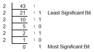
Successive Division is best demonstrated by an example
To get the digits in the right order let them fall to the right.
For this example: 4310 = 1010112 Quick Check (Octal) 101 011 = 5*8 + 3 = 4310
Another example: Convert 4310 from decimal to Octal
For this example: 4310 = 538 Quick Check (Octal) 5*8 + 3 = 4310
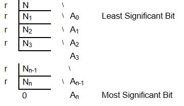
Generalization of the procedure OR Why It Works
Where r = radix, N = number, A = remainder, and n = the number of digits in radix r for number N. Division is normally done in base 10.
Another way of expressing the above table is:
N = r*N1 + A0
N1 = r*N2 + A1
N2 = r*N3 + A2
:
Nn-1 = r*Nn + An-1
Nn = r*0 + An
or (now for the slight of hand)
N = r*( r*N2 + A1)+ A0 substitute N1
N = r2N2 + rA1+ A0 multiply r through equation
N = r2(r*N3 + A2) + rA1+ A0 substitute N2
:
N = Anrn + An-1rn-1 + … + A1r1 + A0r0
Nomenclature
Bit = 1 binary digit
Byte = 8 bits
Nibble = one half byte = 4 bits
Word = Computer Dependent
Arithmetic Operations
Addition
Binary
Binary addition is performed similar to decimal addition using the following binary addition rules:
0 + 0 = 0
0 + 1 = 1
1 + 0 = 1
1 + 1 = 10 (0 with a carry of 1)
Examples:
| Problem | 2110 + 1010 = 3110 | 4510 + 5410 = 9910 | 310 + 710 = 1010 |
| 101012
+ 010102 _______________ 111112 |
1011012
+ 1101102 _______________ 11000112 |
0112
+ 1112 _______________ 10102 |
|
| Check | 1*23 + 0*22 + 1*21 + 0*20 =
1*8 + 0*4 + 1*2 + 0*1 = 1010 |
Octal
Octal addition is also performed similar to decimal addition except that each digit has a range of 0 to 7 instead of 0 to 9.
| Problem | 2110 + 1010 = 3110 | 4510 + 5410 = 9910 | 310 + 710 = 1010 |
| 258
+ 128 _______________ 378 |
558 + 668 _______________ 1438 |
38 + 78 _______________ 128 |
|
| Check | 3*81 + 7*80
3*8 + 7*1 = 3110 |
1*82 + 4*81 + 3*80
64 + 32 + 3 = 9910 |
1*81 + 2*80
8 + 2 = 1010 |
Hexadecimal
Hex addition is also performed similar to decimal addition except that each digit has a range of 0 to 15 instead of 0 to 9.
| Problem | 2110 + 1010 = 3110 | 4510 + 5410 = 9910 | 310 + 710 = 1010 |
|
1516 + 0A16 _______________ 1F16 |
2D16 + 3616 _______________ 6316 |
316 + 716 _______________ A16 (not 10) |
|
| Check | 1*161 + 15*160
16 + 15 = 3110 |
6*161 + 3*160
96 + 3 = 9910 |
10*160
1010 |
Binary Multiplication
| Decimal | Binary |
|
1110 x 1310 _______________ 3310 1110– _______________ 14310 |
10112 x 11012 _______________ 10112 00002- 10112– 10112— _______________ 100011112 |
| Check | 8*161 + 15*160
128 + 15 = 14310 |
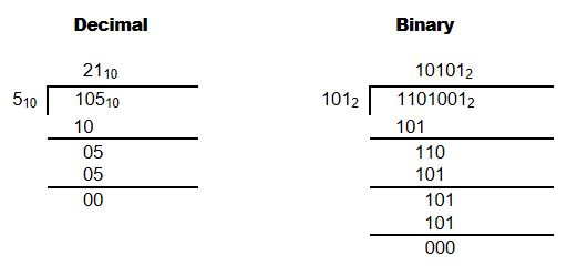
Binary Division
Check: 1*161 + 5*160 = 16 + 5 = 2110
Practice arithmetic operations by making problems up and then checking your answers by converting them back to base 10 via different bases (i.e., 2, 8, and 16).
How a computer performs arithmetic operations is a much more involved subject and has not been dealt with within this section.
Complements and Negative Numbers OR Adding a Sign Bit
Addition, Multiplication, and Division is nice but what about subtraction and negative numbers? From grade school you have learned that subtraction is simply the addition of a negative number. Mathematicians along with engineers have exploited this principle along with modulo arithmetic — a natural outgrowth of adders of finite width — to allow computers to operate on negative numbers without adding any new hardware elements to the arithmetic logic unit (ALU).
Sign Magnitude
Here is a simple solution, just add a sign bit. To implement this solution in hardware you will need to create a subtractor; which means more money.
sign magnitude
Example: – 2 = 1 00102
Ones Complement
Here is a solution that is a little more complex. Add the sign bit and invert each bit making up the magnitude — simply change the 1’s to 0’s and the 0’s to 1’s.
sign magnitude
Example: – 2 = 1 11012
To subtract in 1’s complement you simply add the sign and magnitude bits letting the last carry bit (from the sign) fall into the bit bucket, and then add 1 to the answer. Once again let the last carry bit fall into the bit bucket. The bit bucket is possible due to the physical size of the adder.
0 10102 10
+ _ 1 11012 +(-2)
0 10002 8
+______12 Adjustment
0 10012
Although you can now use your hardware adder to subtract numbers, you now need to add 1 to the answer. This again means adding hardware. Compounding this problem, ones complement allows two numbers to equal 0 (schizophrenic zero).
Twos Complement
Here is a solution that is a little more complex to set up, but needs no adjustments at the end of the addition. There are two ways to take the twos complement of a number.
Method 1 = Take the 1’s complement and add 1
__0 00102 2 <- start
+ 1 11012 1’s complement (i.e. invert)
+ 12 add 1
1 11102
Method 2 = Move from right to left until a 1 is encountered then invert.
| 0 00102 | start = 210 |
| 02 | no change |
| 102 | no change but one is encountered |
| 1102 | invert = change 0 to 1 |
| 11102 | invert = change 0 to 1 |
| 1 11102 | invert = change 0 to 1 |
Subtraction in twos complement is the same as addition. No adjustment is needed, and twos complement has no schizophrenic zero although it does have an additional negative number (see How It Works).
0 10102 10
+ 1 11102 +(-2)
0 10012 8
Examples:
| Problem | 3310 – 1910 = 1410 | 6910 – 8410 = -1510 |
|
0 1000012 + 1 1011012 _______________ 0 0011102 |
0 10001012 + 1 01011002 _______________ 1 11100012 |
|
| Check | convert to intermediate base E16 = 1410 | convert back to sign magnitude
– 00011112 convert to intermediate base (16) – F16 = – 1510 |
Why It Works
Real adders have a finite number of bits, which leads naturally to modulo arithmetic — the bit bucket.
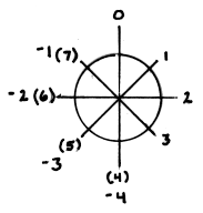
With arithmetic now reduced to going around in circles, positive numbers can add up to negative and vice-versa. Two tests provide a quick check on whether or not an “Overflow” condition exists.
Test 1 = If the two numbers are negative and the answer is positive, an overflow has occurred.
Test 2 = If the two number are positive and the answer is negative, an overflow has occurred.
If computers were calculators and the world was a perfect place, we would be done. But they are not and so we continue by looking at a few real world problems and their solutions.
Character Codes OR Non-Numeric Information
Decimal Number Problems
Represent a Decimal Numbers in a Binary Computer. A binary representation of a decimal number, a few years ago, might have been “hard wired” into the arithmetic logic unit (ALU) of the computer. Today it, more likely than not, is simply representing some information that is naturally represented in base 10, for example your student ID.
Solution
In this problem, ten different digits need to be represented. Using 4 bits 24 or 16 combinations can be created. Using 3 bits 23 or 8 combinations can be created. Thus 4 bits will be required to represent one Decimal Digit. It should here be pointed out how 16 combinations can be created from 4 bits (0000 – 1111) while the largest numeric value that can be represented is 15. The reason that the highest numeric value and the number of combinations are different, is due to zero (0) being one of the combinations. This difference points up the need to always keep track of wetter or not you are working zero or one relative and what exactly you are after — a binary number or combinations.
The most common way of representing a decimal number is named Binary Coded Decimal (BCD). Here each binary number corresponds to its decimal equivalent, with numbers larger than 9 simply not allowed. BCD is also known as an 8-4-2-1 code since each number represents the respective weights of the binary digits. In contrast the Excess-3 code is an unweighted code used in earlier computers. Its code assignment comes from the corresponding BCD code plus 3. The Excess-3 code had the advantage that by complementing each digit of the binary code representation of a decimal digit (1’s complement), the 9’s complement of that digit would be formed. The following table lists each decimal digit and its BCD and Excess-3 code equivalent representation. I have also included the negative equivalent of each decimal digit encoded using the Excess-3 code. For instance, the complement of 0100 (1 decimal) is 1011, which is 8 decimal. You can find more decimal codes on page 18 of “Digital Design” by M. Morris Mano (course text).
| Binary Coded Decimal (BCD) | Excess-3 | |||
| Decimal Digit | Binary Code 8‑4-2-1 | Decimal Digit | Binary Code | 9’s Compliment |
|
0 1 2 3 4 5 6 7 8 9 N/A N/A N/A N/A N/A N/A |
0000
0001 0010 0011 0100 0101 0110 0111 1000 1001 1010 1011 1100 1101 1110 1111 |
N/A
N/A N/A 0 1 2 3 4 5 6 7 8 9 N/A N/A N/A |
0000
0001 0010 0011 0100 0101 0110 0111 1000 1001 1010 1011 1100 1101 1110 1111 |
1111 1110 1101 1100 1011 1010 1001 1000 0111 0110 0101 0100 0011 0010 0001 0000 |
Alphanumeric Character Problem
Represent Alphanumeric data (lower and upper case letters of the alphabet (a-z, A-Z), digital numbers (0-9), and special symbols (carriage return, line feed, period, etc.).
Solution
To represent the upper and lower case letters of the alphabet, plus ten numbers, you need at least 62 (2×26+10) unique combinations. Although a code using only six binary digits providing 26 or 64 unique combinations would work, only 2 combinations would be left for special symbols. On the other hand a code using 7 bits provides 27 or 128 combinations, which provides more than enough room for the alphabet, numbers, and special symbols. So who decides which binary combinations correspond to what character. Here there is no “best way.” About thirty years ago IBM came out with a new series of computers which used 8 bits to store one character (28 = 256 combinations), and devised the Extended Binary-Coded Decimal Interchange Code (EBCDIC pronounced ep-su-dec) for this purpose. Since IBM had a near monopoly on the computer field, at that time, the other computer makers refused to adopt EBCDIC, and that is how the 7bit American Standard Code for Information Interchange (ASCII) came into existence. ASCII has now been adopted by virtually all micro-computer and mini-computer manufacturers. The table below shows a partial list of the ASCII code. Page 23 of the text lists all 128 codes with explanations of the control characters.
| DEC | HEX | CHAR | DEC | HEX | CHAR |
| 32
33 34 35 36 37 38 39 40 41 42 43 44 45 46 47 48 49 50 51 52 53 54 55 56 57 58 59 60 61 62 63 |
20
21 22 23 24 25 26 27 28 29 2A 2B 2C 2D 2E 2F 30 31 32 33 34 35 36 37 38 39 3A 3B 3C 3D 3E 3F |
!
“ # $ % & ‘ ( ) * + , – * / 0 1 2 3 4 5 6 7 8 9 : ; < = > ? |
64
65 66 67 68 69 70 71 72 73 74 75 76 77 78 79 80 81 82 83 84 85 86 87 88 89 90 91 92 93 94 95 |
40
41 42 43 44 45 46 47 48 49 4A 4B 4C 4D 4E 4F 50 51 52 53 54 55 56 57 58 59 5A 5B 5C 5D 5E 5F |
@
A B C D E F G H I J K L M N O P Q R S T U V W X Y Z [ \ ] ^ _ |
The word “string” is commonly used to describe a sequence of characters stored via their numeric codes — like ASCII).
Although ASCII requires only 7 bits, the standard in computers is to use 8 bits, where the leftmost bit is set to 0. This allows you to code another 128 characters (including such things as Greek letters), giving you an extended character set, simply by letting the leftmost bit be a 1. This can also lead to a computer version of the tower of Babel. Alternatively, the leftmost bit can be used for detecting errors when transmitting characters over a telephone line. Which brings us to our next problem.
Synthesis
Although ASCII solves the communication problem between English speaking computers, what about Japanese, Chinese, or Russian computers which have different, and in all these examples, larger alphabets?
Communication Problem
Binary information may be transmitted serially (one bit at a time) through some form of communication medium such as a telephone line or a radio wave. Any external noise introduced into the medium can change bit values from 1 to 0 or visa versa.
Solution
The simplest and most common solution to the communication problem involves adding a parity bit to the information being sent. The function of the parity bit is to make the total number of 1’s being sent either odd (odd parity) or even (even parity). Thus, if any odd number of 1’s were sent but an even number of 1’s received, you know an error has occurred. The table below illustrates the appropriate parity bit (odd and even) that would be appended to a 4-bit chunk of data.
Synthesis
What happens if two binary digits change bit values? Can a system be devised to not only detect errors but to identify and correct the bit(s) that have changed? One of the most common error-correcting codes was developed by R.W. Hamming. His solution, known as a Hamming code, can be found in a very diverse set of places from a Random Access Memory (RAM) circuit to a Spacecraft telecommunications link. For more of error correcting codes read pages 299 to 302 of the text.
Although detecting errors is nice, preventing them from occurring is even better. Which of course brings us to our next problem.
Shaft Encoder Problem
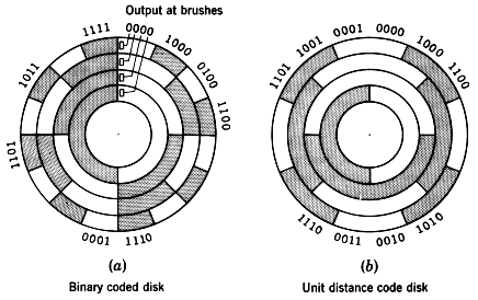
As a shaft turns, you need to convert its radial position into a binary coded digital number.
Solution
The type of coder which will be briefly described below converts a shaft position to a binary-coded digital number. A number of different types of devices will perform this conversion; the type described is representative of the devices now in use, and it should be realized that more complicated coders may yield additional accuracy. Also, it is generally possible to convert a physical position into an electric analog-type signal and then convert this signal to a digital system. In general, though, more direct and accurate coders can be constructed by eliminating the intermediate step of converting a physical position to an analog electric signal. The Figure below illustrates a coded-segment disk which is coupled to the shaft.
The shaft encoder can be physically realized using electro-mechanical (brush) or electro-optical technology. Assuming an electro-optical solution, the coder disk is constructed with bands divided into transparent segments (the shaded areas) and opaque segments (the unshaded areas). A light source is put on one side of the disk, and a set of four photoelectric cells on the other side, arranged so that one cell is behind each band of the coder disk. If a transparent segment is between the light source and a light-sensitive cell, a 1 output will result; and if an opaque area is in front of the photoelectric cell, there will be a O output.
There is one basic difficulty with the coder illustrated: if the disk is in a position where the output number is changing from 011 to 100, or in any position where several bits are changing value, the output signal may become ambiguous. As with any physically realized device, no matter how carefully it is made, the coder will have erroneous outputs in several positions. If this occurs when 011 is changing to 100, several errors are possible; the value may be read as 111 or 000, either of which is a value with considerable errors. To circumvent this difficulty, engineers use a “Gray,” or “unit distance,” code to form the coder disk (see previous Figure). In this code, 2 bits never change value in successive coded binary numbers. Using a Gray coded disk, a 6 may be read as 7, or a 4 as 5, but larger errors will not be made. The Table below shows a listing of a 4-bit Gray code.
| Decimal | Gray Code |
|
0 |
0000 0001 0011 0010 0110 0111 0101 0100 1100 1101 1111 1110 1010 1011 1001 1000 |
Synthesis
Gray code is used in a multitude of applications other than shaft encoders. For example, CMOS circuits draw the most current when they are switching. If a large number of circuits switch at the same time unwelcome phenomena such as “Ground Bounce” and “EMI Noise” can result. If the transistors are switching due to some sequential phenomena (like counting), then these unwelcome visitors can be minimized by replacing a weighted binary code by a Gray code.
If the inputs to a binary machine are from an encoder using a Gray code, each word must be converted to a conventional binary or binary-coded decimal bit equivalent. How can this be done? Before you can answer this question, you will need to learn about Boolean Algebra — what a coincidence, that’s the topic of the next section.
Introduction to the Atmel AVR Family of Microcontrollers
READING
The AVR Microcontroller and Embedded Systems using Assembly and C
by Muhammad Ali Mazidi, Sarmad Naimi, and Sepehr Naimi
Sections: 0.3, 0.4, 1.2, 2.1, 2.2, 2.8, 2.9, 3.3
SOURCE MATERIAL
- Reduced Instruction Set Computer: http://en.wikipedia.org/wiki/Load-store_architecture
- Atmel AVR: http://en.wikipedia.org/wiki/Atmel_AVR
- AVR Quick Reference Guide: http://www.atmel.com/dyn/resources/prod_documents/doc4064.pdf
- ATmega328P Summary (26 pages) http://www.atmel.com/dyn/resources/prod_documents/8161S.pdf
- Arduino Uno schematic
- Arduino shield
- ATmega328P (448 pages) http://www.atmel.com/dyn/resources/prod_documents/doc8161.pdf
- 8-bit AVR Instruction Set (155 pages) http://www.atmel.com/dyn/resources/prod_documents/doc0856.pdf
Table of Contents
WHAT IS A FLIP-FLOP AND A REGISTER
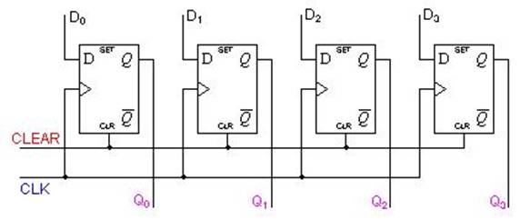
You can think of a D flip-flop as a one-bit memory. As illustrated, the something to remember on the D input of flip-flop is remembered on the positive edge of the clock input.
Truth Table
| Dt | Qt+1 | |
| 0 | 0 | |
| 1 | 1 | |
| x | Qt |
A register is a collection of flip-flops sharing the same clock input.
Labs are based on the ATmega32U4 used in the Arduino Leonardo and Nano. The ATmega328P shown here, is used in the Arduino UNO. For instructional purposes, both architectures will be referenced. The ATmega328P is the simpler of the two architectures and the easier to learn.
THE AVR ENGINE
Let’s adopt the analogy used by Charles Babbage when he called his computer an Analytical Engine. For closer look see this article in Wired and ATmega328 Wikipedia page.
INSTRUCTION SET ARCHITECTURE (ISA)
“The Parts of the Engine”
- The Instruction Set Architecture (ISA) of a microprocessor includes all the registers that are accessible to the programmer. In other words, registers that can be modified by the instruction set of the processor.
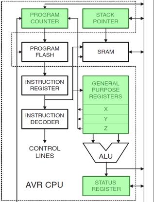
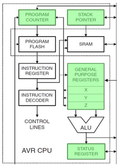
- With respect to the AVR CPU illustrated in Figure 5.2, these ISA registers include the 32 x 8-bit general purpose registers, status register (SREG), the stack pointer (SP), and the program counter (PC).
AVR CPU CORE ARCHITECTURE
“Features of the Engine” Part I
- Reduced Instruction Set Computer (RISC): The instruction set of the computer and target compiler(s) are developed in concert allowing the optimization of both. In this way, a relatively high performance processor can be realized by “reducing” the amount of work any single instruction needs to do; leading to a simpler hardware design (smaller, faster, and cheaper).
8051 Microcontroller ATmega328P Microcontroller cjne A, 0x99, next cmp r16, 0x99
brne next - Mostly 16-bit fixed-length instructions. Instructions have from zero to two operands. Many of today’s RISC microprocessors have up to three operands.
- The Register File of the AVR CPU contains 32 x 8 bit mostly Orthogonal (or identical) General Purpose Registers – instructions can use any register; therefore, simplifying compiler design.
- Load-store memory access. Before you can do anything to data, you must first load it from memory into one of the general-purpose registers. You then use register-register instructions to operate on the data. Finally, you store your answer back into memory.
“Features of the Engine” Part II
- Modified Harvard memory model: A Harvard memory model separates Program and Data memory into separate physical memory systems (Flash and SRAM) that appear in different address spaces. A Modified Harvard memory model has the ability to read/write data items from/to program memory using special instructions. A Princeton memory model computer has only a single address space, shared by both the program and data.
- A Two-stage Instruction Pipeline (fetch and execute) resulting in most instructions being executed in one clock cycle. Consequently, the performance of a 20 MHz processor would approach 20 MIPS (Millions of Instructions Per Second). Compare this with the 8051 Complex Instructions Set Computer (CISC) computer which takes a minimum of 12 clock cycles to execute a single instructions (12 MHz clock = 1 MIPS).
- Simplicity of the computer architecture translates to a faster learning curve and utilization of the machine by the student.
AVR CPU INSTRUCTIONS
“The Language of the Machine”
The Instruction Set of our AVR CPU can be functionally divided (or classified) into five (5) categories.
| Data Transfer | |
| Arithmetic and Logical | |
| Bit and Bit-Test | |
| Control Transfer (Branch Instructions) | “Load the Program Counter” |
| MCU Control | nop, sleep, wdr, break |
- Data Transfer instructions are used to Load and Store data to the General Purpose Registers, also known as the Register File.
-
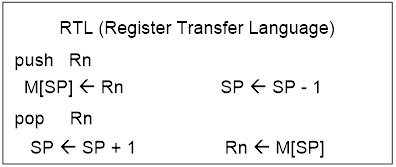
- Exceptions are the push and pop instructions which modify the Stack Pointer.
- By definition these instructions do not modify the status register (SREG).
- Arithmetic and Logic Instructions plus Bit and Bit-Test Instructions use the ALU to operate on the data contained in the general purpose registers .
- Flags contained in the Status Register (SREG) provide important information concerning the results of these operations.
- For example, if you are adding two signed numbers together, you will want to know if the answer is correct. The state of the overflow flag (OV) bit within SREG gives you the answer to this question (1 = error, 0 no error).
- As the AVR processor fetches and executes instructions it automatically increments the program counter (PC) so it always points at the next instruction to be executed. Control Transfer Instructions allow you to change the contents of the PC either conditionally or unconditionally.
- Continuing our example if an error results from adding two signed numbers together we may want to conditionally (OV = 1) branch to an error handling routine.
INSTRUCTION FETCH AND EXECUTE
“The Basic Cycles of the Engine”
Once built, our computer lives to Fetch and Execute instructions, the bread-and-butter of the computer programmer. For this reason, the programmer views the computer as a vehicle for executing a set of instructions. This perspective is codified by the Instruction Set Architecture (ISA) of the computer.
HARVARD VERSUS PRINCETON MEMORY MODEL INSTRUCTION FETCH CYCLE
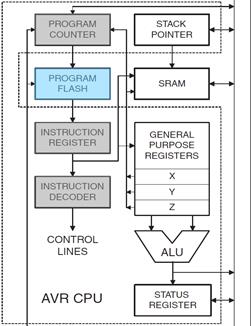
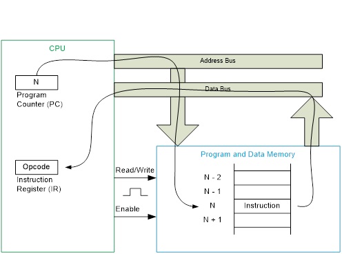
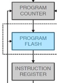
The five (5) steps required to fetch an instruction on a CPU incorporating the Princeton memory model is provided here. The key difference between the Princeton and Harvard memory model is the physical seperation of program memory from data memory. For embedded systems the program memory is implemented using FLASH memory. With program memory now isolated from data memory, the instruction fetch cycle is reduced to a single (1) step. What is accomplished in that single step is shown in bold.
- The CPU presents the value of the program counter (PC) on the address bus and sets the read control line.
- The Flash program memory looks up the address of the instruction and presents the value on the data bus.
- The value from the data bus is placed into the instruction register and the CPU clears the read control line. The instruction register now holds the instruction to be executed.
- The program counter is incremented so it points to the next instruction to be executed.
- The instruction decoder interprets and implements (executes) the instruction.
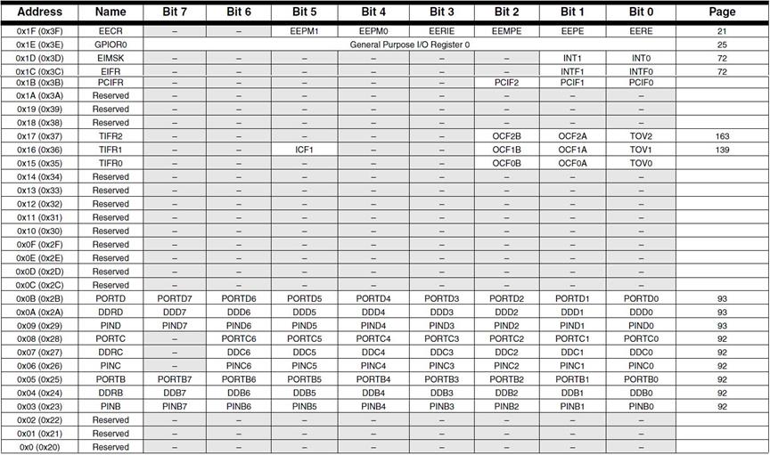
I/O Address Space versus Memory Mapped I/O
- Input and Output ports have traditionally been treated as separate parts of the computer.
- The AVR includes an in instruction to read from an I/O port and an out instruction to write to an I/O port.
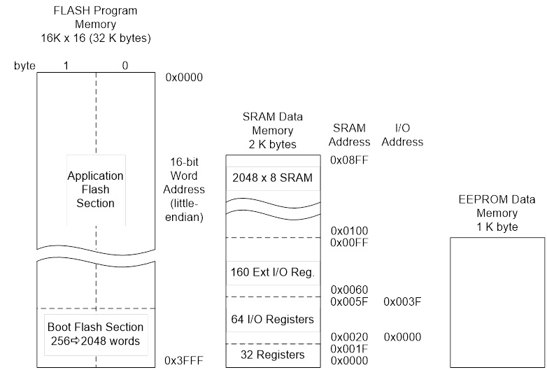
- The AVR has 64 I/O registers accessible to these two instructions
Problem: The Atmel ATmega line of Microcontrollers needs more than 64 I/O registers (GPIO, Timers,…)
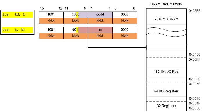
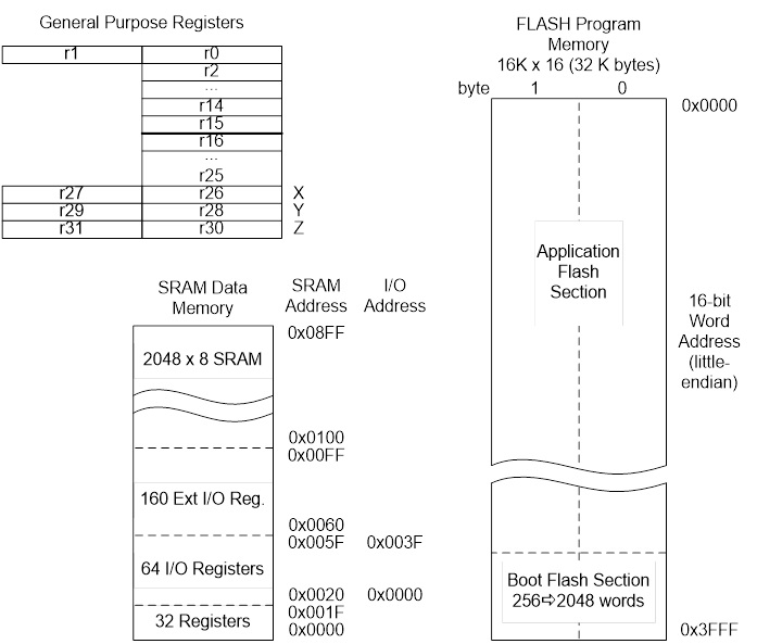
Solution: Instead of looking at computers having 5 basic elements (Input, Output, ALU, CPU, Memory), you can simplify the design to only three (CPU, ALU, and Memory) now allowing the CPU to access 160 “extended” I/O registers using SRAM instructions like lds (load from SRAM) and sts (store to SRAM).
- This was such a powerful technique that Atmel extended the I/O mapping to include the 32 general purpose registers, the original 64 I/O registers, and the 160 extended I/O registers. The overlaying of the I/O address space with the SRAM address space is shown in the next slide.
- A side benefit of the double mapping is the large number of ways of accessing data within SRAM (addressing modes) versus the limited number of instructions and addressing modes available for accessing the original 64 I/O registers (i.e., in, out).
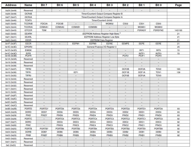
- It is very important to realize that I/O registers are not contiguous within the address space (I/O or SRAM). The mapping is simply a convenient way of accessing registers physically located in diverse locations within the Silicon chip.
Atmel ATmega328P Memory Model
ATMEGA328P I/O MEMORY MAP
Appendix
APPENDIX A PROCESSOR CONTROL AND DATAPATH
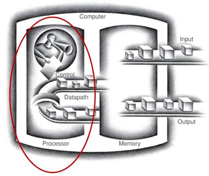
| Control | Datapath |
| Component of the processor that commands the datapath, memory, data, I/O devices according to the instructions of the memory | Components of the processor that perform arithmetic operations and holds data |
APPENDIX B CALCULATING THE LAST ADDRESS
Given a 16K word (2 bytes / word) memory, what is the last address, in hexadecimal?
- The range of memory addresses, like an unsigned number, is from 0 to 2n – 1
- We are given the size of our memory in decimal as 16K10. So the first step is to convert this number to a power of 2.
16K10 = 24 * 210 = 214, which in binary would be… - Which then can directly be expressed as a binary number.

- So the answer is 0x3FFF
- As a short-cut, if you can convert the memory size to a power of 2, the exponent equals the number of 1 in the answer. By dividing the exponent by 4, you have the number of hex digits which are F (11112), with the remainder giving you the most significant hex digit. In our example 4 goes into 14, 3 times with a remainder of 2, where 2 ones (00112) equal hexadecimal 316.
APPENDIX C I/O ADDRESS SPACE VERSUS MEMORY MAPPED I/O
Reading: Your textbook covers memory organization in Section 0.3 “Semiconductor Memory” and I/O Mapping in Section 2.2 “The AVR Data Memory.” The following material covers mapping of the I/O address space in a slightly different way. The material was provided in bullet form earlier in this document.
From Charles Babbage’s Analytical Engine to Dr. Jon Von Neumann’s paper on the EDVAC computer, Input and Output have been treated as separate parts of the computer. Input and Output parts of your PC include the keyboard, mouse, printer, display, etc. To support these “peripheral” devices many microprocessors include a separate I/O address space and instructions for working with the registers contained used to control and access data provided by the peripheral device. For the AVR microcontroller you read an I/O register using an in instruction and write using the out instruction. When Atmel adopted the AVR architecture, they discovered that the 64 I/O registers accessible to these two instructions was insufficient for all the peripheral devices that they were planning on adding to the ATmega line of Microcontrollers. Specifically, they added 160 “extended” I/O registers. However, the AVR microprocessor was only designed for 64 I/O registers. To solve this problem, Atmel turned to an alternative way of working with I/O devices pioneered by Motorola and the 6800 family of processors (among others). Motorola realized that there was no reason to treat input and output devices any different from memory. Now instead of looking at computers having 5 basic elements (Input, Output, ALU, CPU, Memory), you could simplify the design to only three (CPU, ALU, and Memory). Now accessing the 160 “extended” I/O registers was accomplished using SRAM instruction like lds (load from SRAM) and sts (store to SRAM). This was such a powerful technique that Atmel extended the I/O mapping to include the 32 general purpose registers, the original 64 I/O registers, and the 160 extended I/O registers. The overlaying of the I/O address space with the SRAM address space is shown in the next section.
A side benefit of the double mapping is the large number of ways of accessing data within SRAM (addressing modes) versus the limited number of instructions and addressing modes available for accessing the original 64 I/O registers.
It is very important to realize that I/O registers are not contiguous within the address space (I/O or SRAM). The mapping is simply a convenient way of accessing registers physically located in diverse locations within the Silicon chip.
APPENDIX D A BRIEF HISTORY OF THE COMPUTER
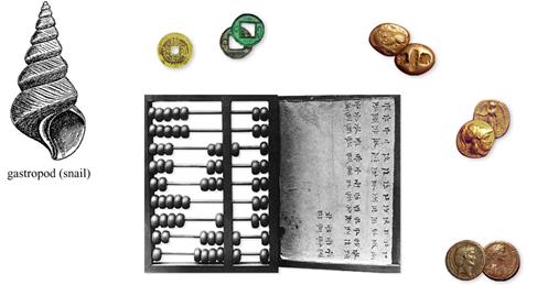
4,000 to 3,000 BC Abacus (+, -, *, /)
- The abacus is an instrument used to perform arithmetic calculations. The positions of beads on a set of wires determine the value of the digit. Romans called these beads calculi the plural of calculus, meaning pebble. This Latin root gave rise to the word calculate. In one contest the Abacus easily won over a mechanical calculator. The abacus is still used in China, Japan, and Korea.
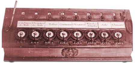
1642 Blaise Pascal Mechanical Calculator (+, -)
- Designed at the age of 20. Rotating wheel mechanical calculator with automatic carry between digits on addition and subtraction of decimal digits (like the odometer in a car). In 1671 Baron von Leibnitz created a calculator, which could add, subtract, and multiply.
- A Human Computer with a mechanical calculator can execute 500 operations a day
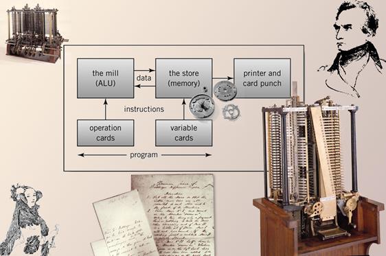
1833 Charles Babbage and the Analytical Engine
- Conceived by Babbage, the engine established the basic principles upon which modern general-purpose digital computers are constructed. This mechanical machine performed instructions dictated by punched cards, with the variable values being determined by a second set of cards. The punched cards came from Joseph Marie Jacquard’s loom, where they controlled the operation of the weaving machines in 1812.
- Neither the Analytical Engine or Difference Engine (1820), a special purpose computer designed to solve polynomial expressions (ex. N2 + N + 41), were ever entirely completed by Babbage known as “the irascible genius.” The difference engine has recently been built as shown here.
1843 Ada Byron and the First Computer Program
- Ada Byron, Lady Lovelace, was one of the most picturesque characters in computer history. Augusta Ada Byron was born December 10, 1815 the daughter of the illustrious poet, Lord Byron. Ada was brought up to be a mathematician and scientist. It was at a dinner party at Mrs. Somerville’s that Ada heard in November 1834, Babbage’s ideas for a new calculating engine, the Analytical Engine. Ada, in 1843, married to the Earl of Lovelace and the mother of three children under the age of eight, wrote an article describing Babbage’s Analytical Engine. Lady Lovelace’s prescient comments included her predictions that such a machine might be used to compose complex music, to produce graphics, and would be used for both practical and scientific use. When inspired Ada could be very focused and a mathematical taskmaster. Ada suggested to Babbage writing a plan for how the engine might calculate Bernoulli numbers. This plan, is now regarded as the first “computer program.” Like her father, she died at 36, Ada anticipated by more than a century most of what we think is brand-new computing.
Source: http://www.scottlan.edu/lriddle/women/love.htm
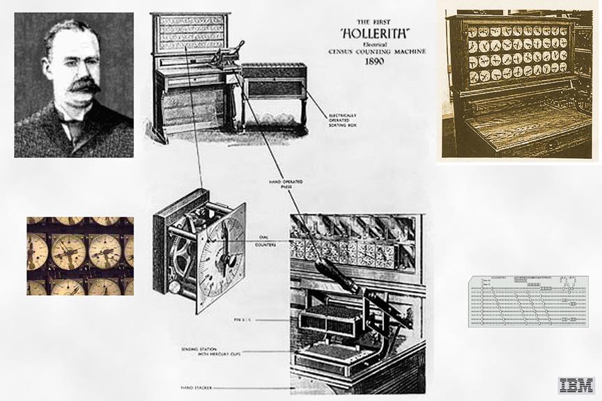
1890 Herman Hollerith and the Census Counting Machine
- Hollerith developed punched cards for tabulating equipment used in the 11th census of the United States. Cards contained 288 locations, size of dollar bill in order to save on tooling. Contact brushes completed electrical circuits allowing the system to do: counting, sensing, punching, and sorting. Started Tabulating Machine Company, which turned into the Computer-Tabulating-Recording Company, which turned into the International Business Machine Corporation (IBM) in 1924.
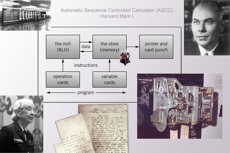
1937 Harvard Mark I
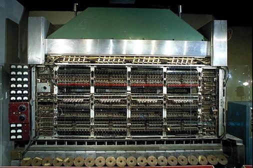
- Howard Hathaway Aiken at Harvard proposed to IBM the Mark I or Automatic Sequence Controlled Calculator — this was to be the first large-scale calculator. Very similar to the Analytical engine, the machine used a combination of electromechanical devices, including many relays. It went to work in 1944 calculating with numbers of 23 digits and computer products of 46-digit accuracy. It received its instructions from perforated tape, from IBM cards, and from the mechanical setting of 1,440 dial switches. Output was either by IBM cards or by typing columns of figures on a roll of paper. The Mark I could perform one division per minute. The machine was in operation for many years, generating many tables of mathematical functions (particularly Bessel functions), and was used for trajectory calculations in World War II.
1943 Electronic Numerical Integrator and Computer (ENIAC)
- Engineers J. Presper Eckert and John W. Mauchly created the ENIAC at the Moore School of Engineering of the University of Pennsylvania between 1943-1946. Built in war time secrecy for the army ordnance department, the ENIAC was designed to do Trajectory calculations. Containing 18,000 vacuum tubes, each accumulator using 100 vacuum tubes arranged as 10 columns of 10 tubes each, the ENIAC could add two 10-digit numbers (the size of ENIAC’s decimal accumulators) in 200 microseconds. Thirty thousand (30,000) times faster than the Mark I. The ENIAC was programmed by patch board and switches. The ENIAC was later moved at a cost of $100,000 to the Ballistic Research Laboratories at the Aberdeen Proving Ground.
1945 Dr. John Von Neumann and the Electronic Discrete Variable Computer (EDVAC)
- EDVAC was the first general-purpose stored program binary electronic (vacuum tube) computer. Completed in 1950 after the EDSAC thus it was not the first operational stored program computer. The technical work done on the EDVAC was by Eckert and Mauchly, Notable the Ultrasonic (or Supersonic) Delay Line, with the logical organization done by Von Neumann, Burke, and Goldstine.

- This computer was the blueprint for most modern day computer systems having in it the 5 principle organs that make up almost all modern day computers. Input, Output, Arithmetical, Central Control, Memory (storing both the numerical as well as the instructional information for a given problem), Eckert as well as others left before the EDVAC was ever completed. Architecturally the EDVAC is classified as a general purpose four address computer.
1947 The First Computer Bug
- American engineers have been calling small flaws in machines “bugs” for over a century. Thomas Edison talked about bugs in electrical circuits in the 1870s. When the first computers were built during the early 1940s, people working on them found bugs in both the hardware of the machines and in the programs that ran them.
- In 1947, engineers working on the Mark II computer at Harvard University found a moth stuck in one of the components. They taped the insect in their logbook and labeled it “first actual case of bug being found.” The words “bug” and “debug” soon became a standard part of the language of computer programmers.
1951 John Von Neumann and Princeton’s IAS (Institute for Advance Study) Machine
- Designed to develop a world weather model, the IAS machine incorporated most of the general concepts of parallel binary stored-program computers. That is it used random access memory or parallel memory, CRTs. One address computer.
1951 Eckert and Mauchly and the UNIVAC I
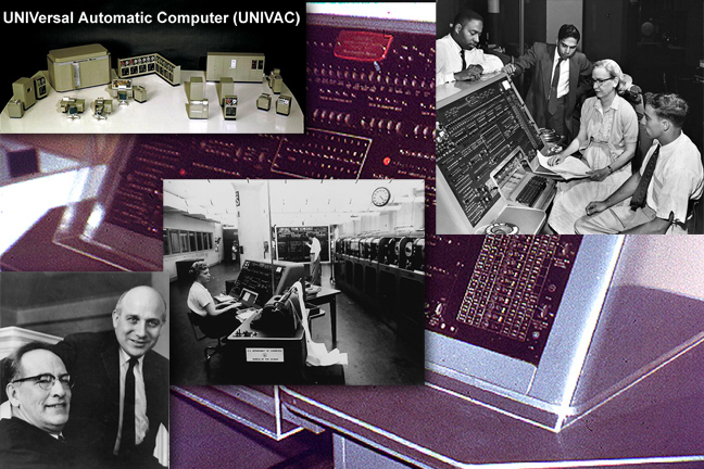
- Soon after the formal dedication of ENIAC computer, J. Presper Eckert and John W. Mauchley’s left the University of Pennsylvania to start their own business. Early orders from U.S. government agencies and other potential customers were not enough to keep the young Eckert-Mauchley Computer Corporation alive, and Remington Rand agreed to purchase the firm in 1950. Work on the UNIVAC I (Universal Automatic Computer) went forward, and the first commercially available electronic (vacuum tube) digital computer was delivered to the Bureau of the Census in early 1951. By 1957, some 46 copies of the machine had been installed at locations ranging from the David Taylor Model Basin of the U.S. Navy Bureau of Ships, to Pacific Mutual Life Insurance Company, to the offices of the Commonwealth of Pennsylvania.
- The UNIVAC, like the ENIAC, had vacuum tube circuit elements. There also were some 18,000 crystal diodes. Central memory was handled in acoustic delay-line tanks, which were used in several early computers. UNIVAC also had an external magnetic tape memory, as well as magnetic tapes used in input and output. Users of UNIVAC played an important role in the development of programming languages. Source: Smithsonian Computer History Collection
1965 Digital Equipment Corporation (DEC) PDP-8
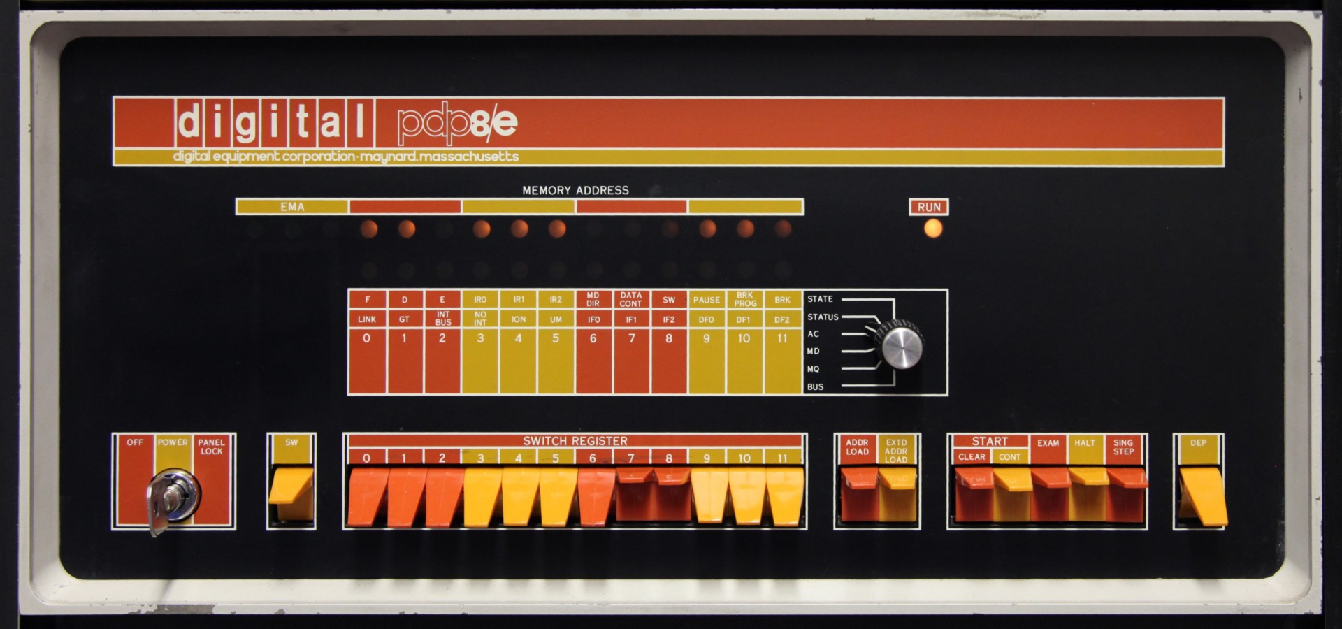
- Designed using Integrated Circuits, DEC sold the first PDP-8 for only $18,000. Later versions of this machine that incorporated improvements in electronics appeared over the next decade. These became steadily smaller and cheaper, triggering a rush of new applications in which the computer was embedded into another system and sold by a third party (called an Original Equipment Manufacturer, or OEM). Some machines were specifically designed for time sharing and for business applications. Ultimately over 50,000 PDP-8’s were sold (excluding those embedded as single chips into other systems) bringing computers into the laboratory and the manufacturing plant’s production line, and thus the minicomputer industry was born. (read “The Sole of a New Machine”).
The x86 isn’t all that complex — it just doesn’t make a lot of sense
Mike Johnson
Leader of the 80×86 Design at AMD
Microprocessor Report (1994)
June 1969 to April 1971 Ted Hoff and Intel 3-chipset 4004
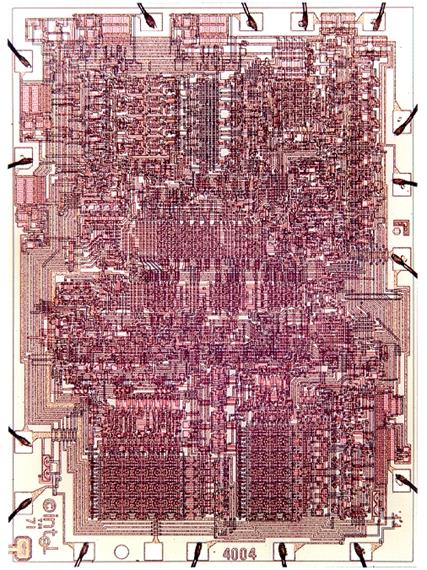
- Intel, a company founded in 1968, is asked by Busicom of Japan to design a custom LSI calculator chip-set. Intel discovers design will take 11 36-40 pin IC packages and proposes a creative alternative. Ted Hoff, at Intel, had been working with the PDP-8 min-computer and proposed to Busicom that a general purpose LSI chip-set be designed that could be programmed to be a calculator or for other applications. We are so used to using computers, that the genus of this step can escape us. The traditional solution was to design what you wanted using logic gates. What Ted Hoff envisioned was a wholly different approach. You design a simple CPU and taught it using software to do what you want. Today these computers are known a microcontrollers and embedded systems. Publicly announced on November 1971.
Nov 1969 to Jan 1972 Vic Poor and the Intel 8008
- Vic Poor of Datapoint Corporation of San Antonio, Texas (manufacturers of “intelligent terminals” and small computer systems) along with Cogar and Viatron engineers design a very elementary computer, and put under contract Intel and Texas Instruments to implement the design on a single logic chip. Intel succeeded, but their product executed instructions approximately ten (10) times as slowly as Datapoint had specified and way behind schedule (work had been stopped by Intel to complete the Busicom chip-set.); so Datapoint declined to buy it, and built their own product using existing logic components. And thus Intel holding a computer-like logic device (whose development had been paid for) marketed the Intel 8008 and the microcomputer industry was born.
1975 John Cocke and the IBM 801
- The first (Reduced Instruction Set Computer) RISC machine was developed as part of the IBM 801 Minicomputer Project. John Cocke contributed many detailed innovations in the 801 processor and associated optimizing compiler, and is considered the “father of RISC architecture.”
- “John’s concept of the RISC resulted from his detailed study of the trade-offs between high performance machine organization and compiler optimization technology. He recognized that an appropriately defined set of machine instructions, program controls, and programs produced by a compiler — carefully designed to exploit the instruction set — could realize a very high performance processor with relatively few circuits. Critical to the success of RISC was the concept of an optimizing compiler able to use the reduced instruction set very efficiently and maximize performance of the machine.”
Source: http://domino.watson.ibm.com/comm/pr.nsf/pages/news.20020717_cocke.html
1976 Intel i8748
- Prior to 1976 small board computers (SBCs) were designed around microprocessor chips, like the 8080. These SBCs included all the features needed to implement a very simple computer system. These SBCs, of which the D2 by Motorola, KIM-1 by MOS Technology, and SDK-85 by Intel are the most memorable, quickly found their way into design labs at colleges, universities, and electronic companies. By adding peripheral cards these SBCs could read sensors and control actuators. In 1976 Intel put all of the features found on an SBC and parts of the peripheral cards into one chip known as the i8748. With over 17,000 transistors the i8748 was the first device in the MCS-48 family of microcontrollers. This IC, and other MCS-48 devices, quickly became the de facto industrial standard in control-oriented applications. Soon MCS-48 devices were replacing electromechanical components in many modern appliances.
1980 Intel 8051
- With over 60,000 transistors, the power, size, and complexity of microcontrollers moved to the next level with Intel’s introduction of the 8051, the first device in the MCS-51 family of microcontrollers. In a bold move, Intel allowed other manufacturers to make and market code-compatible variants of the 8051. This step led to its general acceptance by the engineering community as the de facto standard in microcontroller architectures.
1996 Atmel AVR
- AVR is a moniker for a family of Atmel 8-bit RISC microcontrollers. The AVR is a Modified Harvard architecture machine with program and data stored in separate physical memory systems that appear in different address spaces. The AVR architecture was conceived by Alf-Egil Bogen and Vegard Wollan at the Norwegian Institute of Technology (NTH). When the technology was sold to Atmel, the internal architecture was further developed by Alf and Vegard at Atmel Norway, a subsidiary of Atmel founded by the two architects. The name AVR sounds cool and does not stand for anything.
Source: http://en.wikipedia.org/wiki/Atmel_AVR
APPENDIX E CLASSIC COMPUTER ARCHITECTURE
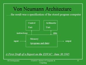
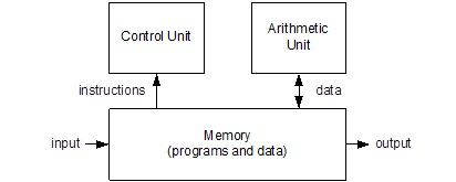
As we discovered in our short history lesson, computers are designed to meet a specific set of requirements. In the early days, these requirements were to meet some military, science, civil, or commercial need. For the military, it was predominately the calculation of ballistic tables; for science to calculate the motion of the planets or the weather. For civil keeping track of people and commercial keeping track of the money. To meet these requirements the computer was conceived and described by its (1) hardware components and (2) the instructions it could execute. The former, for all modern day computers, were codified by Von Neumann in his landmark paper describing the architecture of the EDVAC computer.
Von Neumann’s paper describes a computer architecture having five basic components: Input, Output, Memory, Control, and Arithmetical.
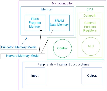
For this class we will Reparation these elements as discussed in the next section and defined in Figure 1-3. An important component of this new viewpoint is the central processing unit (CPU) which will be divided into a Control and a Datapath element as shown in the Figure 1-2. Atmel literature uses the term microcontroller unit (MCU) in place of the more generic central processing unit. In this course the two terms are considered synonymous.
Classic Microcontroller Architecture
The CPU is divided into a Control and a Datapath element as shown in the Figure 1-2. The Control Unit contains combination logic and translates the instructions held in the instruction register (not shown) into the control signals needed to execute the instruction. The data path contains the General Purpose Registers (technically known as the Register File) and the Arithmetic and Logic Unit (ALU). The Datapath includes a few other registers which we will learn about shortly.
The integration of the program and data memory described by Von Neumann is today known as the Princeton memory model. The architecture of our AVR processor separates these two types of memory into Flash Program Memory and Static Random Memory (SRAM). This separation of program and data memory more resembles the Harvard Mark I computer, than the EDVAC computer, and is therefore known as the Harvard memory model.
The input and output functions of Figure 1-1 will be treated together and simply called input/output (I/O). For microcontrollers, the term I/O includes all the Peripherals (Parallel I/O, Counter/Timers, etc.) supported by a particular model of microcontroller, in our case the ATmega328P.
For this class the Von Neumann architecture is thus repartitioned into five basic blocks: Flash Program Memory, SRAM Data Memory, Control Unit, Datapath, and Input-Output.
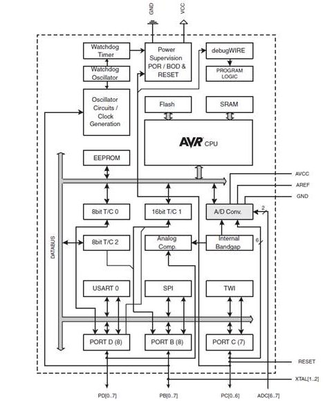
APPENDIX F ATMEGA328P ARCHITECTURAL OVERVIEW
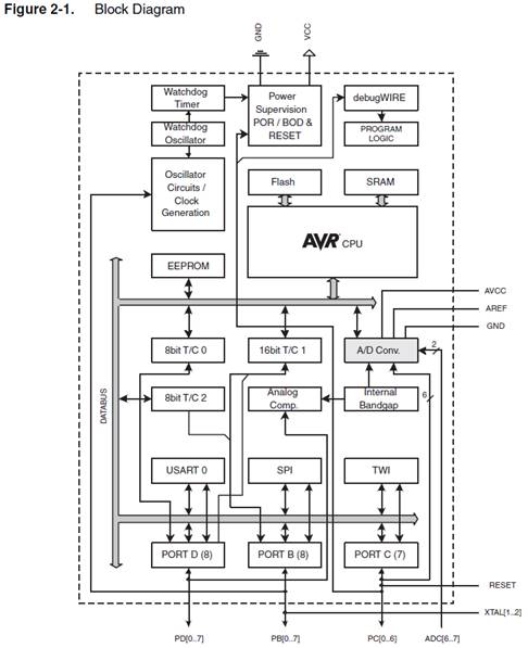
Reading: Section 5.1 Overview plus Atmega8 Block Diagram
Clock
- ATmega Family – Up to 20 MHz
- Arduino Duemilanove – 16 MHz (ATmega328P)
- ALU – On-chip 2-cycle Hardware Multiplier
Memory
- ATmega Family – Up to 256 KBytes Flash, 4K Bytes EEPROM and 8K Bytes SRAM.
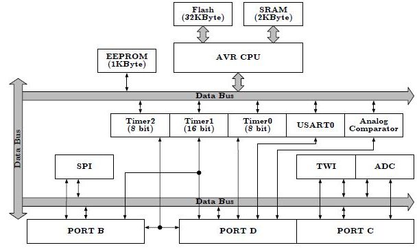
- ATmega328P – 32 KBytes Flash, 1K Bytes EEPROM, and 2K Bytes SRAM
- Self-Programming Flash memory with boot block (ICSP header)
Peripheral Subsystems
- Two 8-bit (PORTB, PORTD), plus One 7-bit (PORTC) General Digital I/O Ports
- Programmable Serial USART, Master/Slave SPI Serial Interface.
- Byte-oriented 2-wire Serial Interface (TWI) is Philips I2C compliant.
- Two 8-bit Timer/Counters with Separate Prescaler and Compare Mode
- One 16-bit Timer/Counter with Separate Prescaler, Compare Mode, and Capture Mode
- Six PWM Channels
- 8-channel 10-bit A/D converter with up to x200 analog gain stage.
- Programmable Watchdog Timer with Separate On-chip Oscillator
- On-Chip Debug through JTAG or debugWIRE interface.
Other Features
- External and Internal Interrupt Sources with 2 instruction words/vector
Note
- In the following Block Diagram, Power (Vcc), Ground (GND), and the clock input (XTAL) are present but not shown.
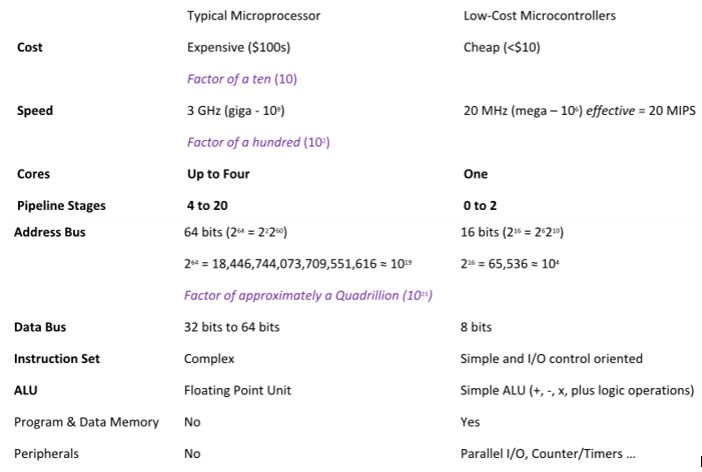
APPENDIX G MICROPROCESSOR VERSUS MICROCONTROLLER
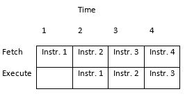
APPENDIX H TWO-STAGE INSTRUCTION PIPELINE
Pipelining: A technique that breaks operations, such as instruction processing or bus transactions, into smaller distinct stages or tenures (respectively) so that a subsequent operation can begin before the previous one has completed.
From the Atmel ATmega328P Data Sheet Chapter 6 AVR CPU Core, Section 6.1 Overview and with respect to Figure 6-1 Block Diagram of the AVR Architecture
“In order to maximize performance and parallelism, the AVR uses a Harvard architecture – with separate memories and buses for program and data. Instructions in the program memory are executed with a single level pipelining. While one instruction is being executed, the next instruction is pre-fetched from the program memory. This concept enables instructions to be executed in every clock cycle. The program memory is In-System Reprogrammable Flash memory.”
A pipeline stage begins and ends with a register; controlled by a clock. Between the register(s) is combinational logic. Although counter-intuitive, Flash program memory can be viewed as combinational logic with an address generating a word of data. With respect to our AVR architecture (Figure 6-1) the two registers of interest are the Program Counter (PC) and the Instruction Register (IR). Without pipelining these two registers in the control unit (PC, IR) would require two clock cycles to complete a basic computer operation cycle. Specifically, an instruction is (1) fetched and then (2) executed.
For most instructions, especially one based on a modified Harvard memory model, program memory is not accessed during the execution cycle. This memory down time could be used to fetch the next instruction to be executed, in parallel with the execution cycle of the current instruction. Here then is an opportunity for pipelining! Figure 10.2 illustrates the idea. The pipeline has two independent stages. The first stage fetches an instruction and places it in the Instruction Register (IR), while the second stage is executing the instruction. This two-stage instruction pipeline is also called instruction prefetch can be found in some of the earliest microprocessors including the Intel 8086
For our RISC architecture most instructions are executed in a single cycle (also known as elemental instructions). In this perfect world where all instructions take one cycle to fetch and one cycle to execute, after an initial delay of one cycle to fill the pipeline, known as latency, each instruction will take only one cycle to complete.
Forgetting for now the circuit delays attendant with implementing the pipeline (for example the latch), and other complicating issues, our performance would be twice that of a non-pipelined design.
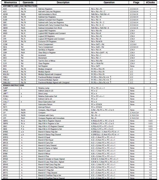
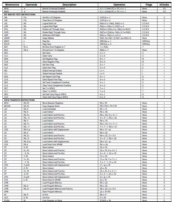
APPENDIX I ATMEGA328P INSTRUCTION SET
The Instruction Set of our AVR processor can be functionally divided (or classified) into the following types:
- Data Transfer Instructions
- Arithmetic and Logic Instructions
- Bit and Bit-Test Instructions
- Branch (Control Transfer) Instructions
- MCU Control Instructions
Addressing Modes: Working with AVR’s Load-Store RISC Architecture
READING
The AVR Microcontroller and Embedded Systems using Assembly and C
by Muhammad Ali Mazidi, Sarmad Naimi, and Sepehr Naimi
Sections: 2.3, 6.2
Table of Contents
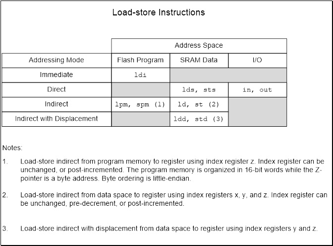
LOAD-STORE INSTRUCTIONS AND THE ATMEGA328P MEMORY MODEL
When selecting an addressing mode you should ask yourself where is the operand (data) located within the memory model of the AVR processor and when do I know its address (assembly time or at run time).
LOAD-STORE INSTRUCTIONS AND ADDRESSING MODES
- When loading and storing data we have several ways to “address” the data.
- The AVR microcontroller supports addressing modes for access to the Program memory (Flash) and Data memory (SRAM, Register file, I/O Memory, and Extended I/O Memory).
IMMEDIATE
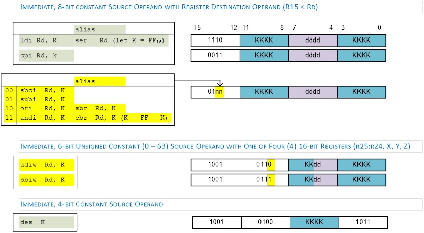
- Data is encoded with the instruction. Operand is therefore located in Flash Program Memory. This is why technically our memory model is a Modified Harvard.
ldi r16, 0x23 // where ldi = 1110, Rd = 00002, and constant K = 001000112
- Notice that only four bits (dddd) are set aside for defining destination register Rd. This limits us to 24 = 16 registers. The designers of the AVR processor chose registers 16 to 31 to be these registers (i.e., 16 ≤ Rd ≤ 31).
DIRECT
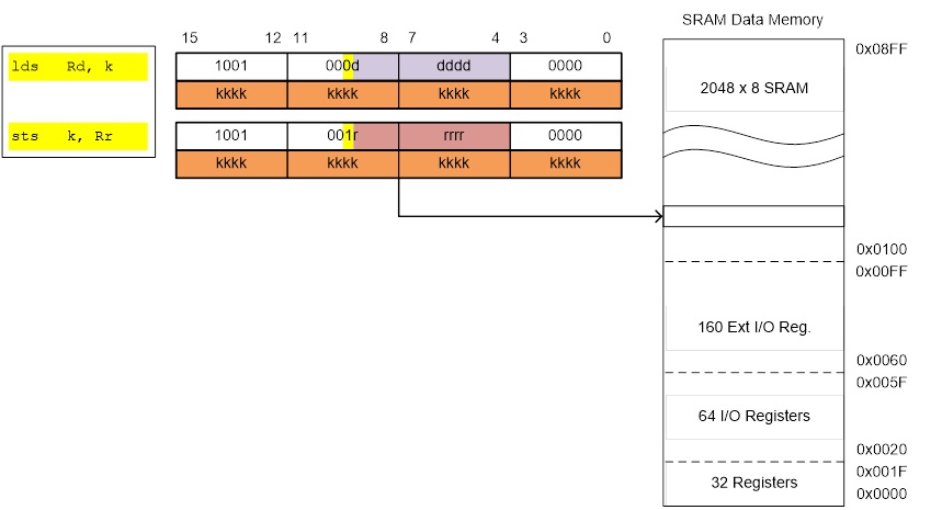
lds r16, A
sts A, r16
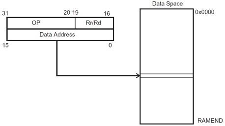
Within the AVR family there are two (2) possible lds/sts instructions. A specific family member will have only one lds/sts combination. The ATmega328P lds/sts instruction is illustrated here with the exception that 5 bits (not 4) encode Rr/Rd. This means all 32 registers are available to the lds/sts instruction.
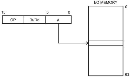
in r16, PINC
out PORTD, r16
REGISTER-REGISTER INSTRUCTIONS
Data Transfer
- Register-register move byte (mov) or word (movw)
Arithmetic and Logic (ALU)
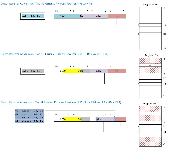
- Two’s complement negate (neg), Arithmetic add (add, adc, adiw), subtract (sub, subi, sbc, sbci), and multiply (mul, muls, mulsu, fmul, fmuls, fmulsu)
- Logical not (com), and (and, andi, cbr, tst), or (or, ori, sbr), exclusive or (eor)
- Clear (clr), set (ser), increment (inc), decrement (dec)
Bit and Bit-Test
- Register logical shift left (lsl) or right (lsr); arithmetic shift right (asr); and rotate left or right (rol, ror)
- Register swap nibble (swap)
- Register bit load (bld) or store (bst) from/to T flag in the Status Register SREG
- I/O Register Clear (cbi) or set (sbi) a bit
- Clear (clFlag) or set (seFlag) a Flag bit in the Status Register SREG by name (I, T, H, S, V, N, Z, C) or bit (bclr, bset).
REGISTER DIRECT
In the following figures, OP means the operation code part of the instruction word. To simplify, not all figures show the exact location of the addressing bits. To generalize, the abstract terms RAMEND and FLASHEND have been used to represent the highest location in data and program space.
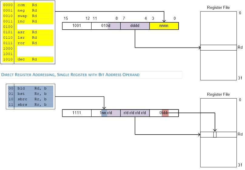
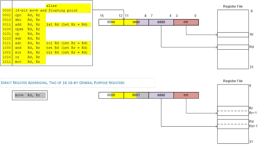
com r16
add r16, r17
LOAD-STORE PROGRAM EXAMPLE
Write an Assembly program to add two 8-bit numbers.
C = A + B
lds r16, A ; 1. Load variables
lds r17, B
add r16, r17 ; 2. Do something
sts C, r16 ; 3. Store answer
- Identify the operation, source operand, destination operand in the first Data Transfer instruction.
- Identify the source/destination operand in the Arithmetic and Logic (ALU) instruction.
- What addressing mode is used by the source operand, in the first instruction?
- Show contents of Flash Program Memory (mnemonics)
- Show contents of SRAM Data Memory, assuming variables are stored in sequential memory locations starting at address 010016.
- Modify the program to leave register r16 unchanged by making a copy (use r15).
SPECIAL TOPIC – HARVARD VERSUS PRINCETON ARCHITECTURE
Princeton or Von Neumann Memory Model
Program and data share the same memory space. Processors used in all personal computers, like the Pentium, implement a von Neumann architecture.
Harvard Memory Model
Program and data memory are separated. The AVR processors among others including the Intel 8051 use this memory model. One advantage of the Harvard architecture for microcontrollers is that program memory can be wider than data memory. This allows the processor to implement more instructions while still working with 8-bit data. For the AVR processor program memory is 16-bits wide while data memory is only 8-bits.
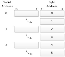
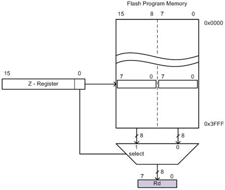
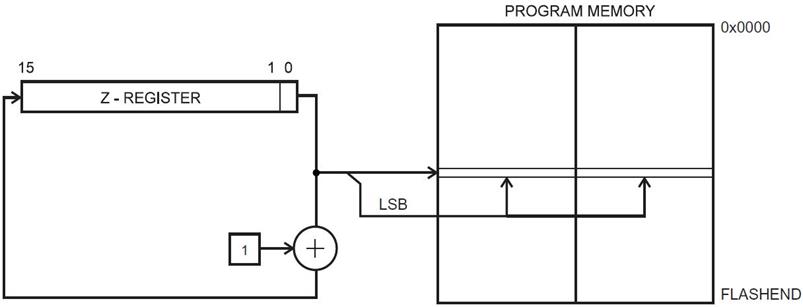
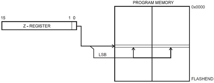
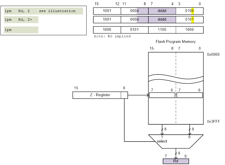
You may have already noticed that when you single step your program in the simulator of AVR Studio it is incremented by 1 each time an instruction is executed. No surprise there right? Wrong. The program memory of the AVR processor can also be accessed at the byte level. In most cases this apparent paradox is transparent to the operation of your program with one important exception. When you want to access data stored in program memory, you will be working with byte addresses not words (16-bits). The assembler is not smart enough to know the difference and so when you ask for an address in program memory it returns its word address. To convert this word address into a byte address you need to multiply it by 2. Problematically we do this by using the shift left syntax of C++ to explicitly tell the assembler to multiply the word address by 2. Remember, when you shift left one place you are effectively multiplying by 2.
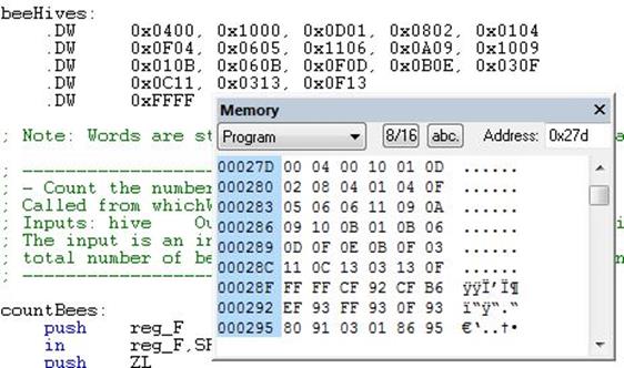
With this in mind, we would interpret the following AVR instruction as telling the AVR assembler to convert the word address of label beehives in program memory to a byte address and then to take the low order of the resulting value and put into the source operand of the instruction.
ldi ZL,low(beeHives<<1) // load word address of beeHives look-up
APPENDIX A – ATMEGA328P INSTRUCTION SET
Introduction to AVR Assembly Language Programming II: ALU and SREG
READING
The AVR Microcontroller and Embedded Systems using Assembly and C
by Muhammad Ali Mazidi, Sarmad Naimi, and Sepehr Naimi
Sections: 2.4, 5.1, 5.2, 6.5
COMPLEMENTARY READING
The following source(s) cover the same material as Chapter 2 of your textbook.
They are provided to you in case you want a different viewpoint.
ATMEL document doc8161 “8-bit AVR Microcontroller with 4/8/16/32K Bytes In-System Programmable Flash” Section 6.3.1: SREG – AVR Status Register
Table of Contents
INSTRUCTION SET ARCHITECTURE (REVIEW)
ALU – TWO OPERAND INSTRUCTIONS
- All math (+,-,×,÷) and logic (and, or, xor) instructions work with the Register File (register to register).
- Most math and logic instructions have two operands Rd, Rr with register Rd initially containing one of the values to be operated on and ultimately the result of the operation. The initial contents of Rd are therefore destroyed by this operation.
add Rd, Rr ; Rd = Rd + Rr, You may use any register (R0 – R31).
- Some math and logic operations replace the source register Rr with a constant K. Typically denoted by an “i” postfix.
subi Rd, K ; Rd = Rd – K, You may only registers (R16 – R31).
add, adc, adiw Adds two registers and the contents of the C Flag (adc only) and places the result in the destination register Rd.
sub, sbc, subi, sbci, sbiw Subtracts the source register Rs or constant K from the source/destination register Rr and subtracts with the C Flag (sbc and sbci only) and places the result in the source/destination register Rd. Think of the C Flag as the Borrow bit within this context.
mul, muls, mulsu, fmul, fmuls, fmulsu The multiplicand Rd and the multiplier Rr are two registers containing binary or fractional ( f-prefix) encoded numbers. Both numbers may be unsigned (mul, fmul), or signed (muls, fmuls). Finally, the multiplicand Rd may be signed with the multiplier Rr unsigned (mulsu, fmulsu). The 16-bit unsigned product is placed in R1 (high byte) and R0 (low byte).
and, andi, or, ori, eor Performs the logical AND, OR, and XOR operations between the contents of register Rd and register Rr or constant K.
ALU – SINGLE OPERAND INSTRUCTIONS
- All single operand math and logic instructions only need a single register and usually the mnemonic alone is enough to tell you what it does.
| Mnemonic | Operation | Description |
| com | One’s complement | |
| neg | Two’s complement | |
| inc | Increment | |
| dec | Decrement | |
| clr | Clear | |
| ser | Set Register, Limited to r16-r31 | |
| tst | Test for Zero or Minus |
ALU PROGRAM EXAMPLE
Write an Assembly program to implement the polynomial expression
B = A2 + A + 41
.INCLUDE
.DSEG
A: .BYTE 1 // 8 bit input
B: .BYTE 2 // 16 bit output
.CSEG
; load
lds r16, A ; r16 with the value of A
clr r17 ; r17 with 0
ldi r18, 41 ; r18 with 41
; do something
mul r16, r16 ; r1:r0 = A^2
add r0, r16
adc r1, r17 ; r1:r0 = A^2 + A
add r0, r18
adc r1, r17 ; r1:r0 = A^2 + A + 41
; store
sts B, r0 ; answer byte ordering
sts B+1, r1 ; is little endian
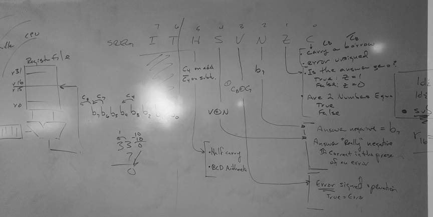
SREG – AVR STATUS REGISTER
SREG – AVR Status Register
Non ALU
- Bit 7 – I: Global Interrupt Enable
The Global Interrupt Enable bit must be set for the interrupts to be enabled. The individual interrupt enable control is then performed in separate control registers. The I-bit is cleared by hardware after an interrupt has occurred, and is set by the reti instruction. The I-bit can also be set and cleared by the application with the sei and cli instructions. - Bit 6 – T: Bit Copy Storage
The Bit Copy instructions bld (Bit LoaD) and bst (Bit STore) use the T-bit as source or destination. A bit from a register can be copied into T (Rb -> T) by the bst instruction, and a bit in T can be copied into a bit in a register (T -> Rb) by the bld instruction.
ALU
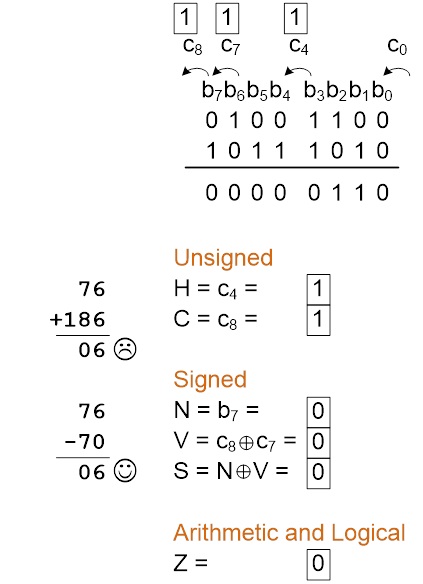
Signed two’s complement arithmetic
- Bit 4 – S: Sign Bit, S = N ⊕ V
Bit set if answer is negative with no errors or if both numbers were negative and error occurred, zero otherwise. - Bit 3 – V: Two’s Complement Overflow Flag
Bit set if error occurred as the result of an arithmetic operation, zero otherwise. - Bit 2 – N: Negative Flag
Bit set if result is negative, zero otherwise.
Unsigned arithmetic
- Bit 5 – H: Half Carry Flag
Carry from least significant nibble to most significant nibble. Half Carry is useful in BCD arithmetic. - Bit 0 – C: Carry Flag
The Carry Flag C indicates a carry in an arithmetic operation. Bit set if error occurred as the result of an unsigned arithmetic operation, zero otherwise.
Arithmetic and Logical
- Bit 1 – Z: Zero Flag
The Zero Flag Z indicates a zero result in an arithmetic or logic operation.
THE SREG OVERFLOW BIT
- The overflow bit indicates if there was an error caused by the addition or two n-bit 2’s complement numbers, where the n-1 “sign bit” is 1 if the number is negative and 0 if the number is positive. In other words, the sum is outside the range 2n 1 to 2n 1 1.
- Another way to recognize an error in addition is to observe that if you add two numbers of the same sign (positive + positive = negative or negative + negative = positive) then an error has occurred.
- An overflow condition can never result from the addition of two n-bit numbers of opposite sign (positive _ negative or negative + positive).
- Here are examples of all four cases for two 8 bit signed numbers.
Case A B C D 0b6b5b4b3b2b1b0 0b6b5b4b3b2b1b0 1b6b5b4b3b2b1b0 1b6b5b4b3b2b1b0 0b6b5b4b3b2b1b0 1b6b5b4b3b2b1b0 0b6b5b4b3b2b1b0 1b6b5b4b3b2b1b0
The variable “bn” simply indicates some binary value and may be 1 or 0. The index of the carry bit (Cn) is equal to the carry into bit bn. For example, the carry into b0 is C0 and the carry out of an 8-bit register b7 is C8.
- Looking first at Case A, a carry cannot be generated out of the sign bit (Cn+1=0); therefore, if a carry enters the sign bit (Cn=1), the sum will be negative and the answer is wrong.
- For Case B and Case C no error can occur. Observe that in both case B and C because the numbers are contained in an n-bit (n = 8) register, we know they are in the range -2n-1 to 2n-1-1 (-128 to 127 for our two 8-bit numbers). Because one number is positive and the other negative, we further know, the answer must be correct.
- For Case D, a carry will always be generated out of the sign bit Cn+1=1 (ex. C8 = 1) with the sign bit itself set to 0; therefore, if a carry does not enter the sign bit Cn=0 (C7=1) the sum will be positive and the answer will be wrong.
- Here is what we have discovered translated into a truth-table.

- Solving for the overflow bit (V) we have,
COMPUTING ALU STATUS REGISTER BITS – ADDITION –
COMPUTING ALU STATUS REGISTER BITS – SUBTRACTION –
- For subtract instructions (sub, subi, sbc, sbci, sbiw), including compare instructions (cp, cpc, cpi, cpse), the carry bit is equal to
and
- Assume the subtract instruction sub r16, r17 has just been run by the ATmega328P microcontroller. Complete the table provided. The “difference” column should reflect the contents of register r16 after the subtraction operation (leave the answer in 2’s complement form) and not the actual difference (i.e., if done using your calculator).
Signed Unsigned r16 r17 difference relationship relationship H S V N Z C 3B 3B 00 + = + = 0 0 0 0 1 0 3B 15 26 + > + > 0 0 0 0 0 0 15 3B F9 F6 F6 F9 15 F6 F6 15 68 A5 A5 68 - Use AVR Studio simulation software to check your answers.
Introduction to AVR Assembly Language Programming II: Branching
READING
The AVR Microcontroller and Embedded Systems using Assembly and C
by Muhammad Ali Mazidi, Sarmad Naimi, and Sepehr Naimi
Sections: 3.1
ADDITIONAL READING
Introduction to AVR assembler programming for beginners, controlling sequential execution of the program http://www.avr-asm-tutorial.net/avr_en/beginner/JUMP.html
Table of Contents
INSTRUCTION SET ARCHITECTURE (REVIEW)
The Instruction Set Architecture (ISA) of a microprocessor includes all the registers that are accessible to the programmer. In other words, registers that can be modified by the instruction set of the processor. With respect to the AVR CPU illustrated here , these ISA registers include the 32 x 8-bit general purpose resisters, status resister (SREG), the stack pointer (SP), and the program counter (PC).
Data Transfer instructions are used to load and store data to the General Purpose Registers, also known as the Register File. Exceptions are the push and pop instructions which modify the Stack Pointer. By definition these instructions do not modify the status register (SREG).
Arithmetic and Logic Instructions plus Bit and Bit-Test Instructions use the ALU to operate on the data contained in the general purpose registers. Flags contained in the status register (SREG) provide important information concerning the results of these operations. For example, if you are adding two signed numbers together, you will want to know if the answer is correct. The state of the overflow flag (OV) bit within SREG gives you the answer to this question (1 = error, 0 no error).
Control Transfer Instructions allow you to change the contents of the PC either conditionally or unconditionally. Continuing our example if an error results from adding two signed numbers together we may want to conditionally (OV = 1) branch to an error handling routine. As the AVR processor fetches and executes instructions it automatically increments the program counter (PC) so it always points at the next instruction to be executed.
INSTRUCTION SET (REVIEW)
The Instruction Set of our AVR processor can be functionally divided (or classified) into the following parts:
- Data Transfer Instructions
- Arithmetic and Logic Instructions
- Bit and Bit-Test Instructions
- Control Transfer (Branch) Instructions
- MCU Control Instructions
JUMP INSTRUCTIONS
- There are two basic types of control transfer instructions – Unconditional and Conditional.
- From a programmer’s perspective an unconditional or jump instruction, jumps to the label specified. For example, jmp loop will unconditionally jump to the label loop in your program.
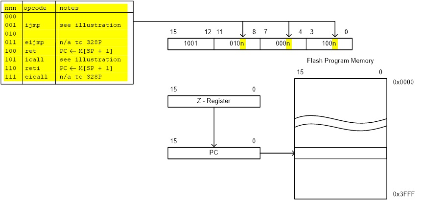
- Here are the unconditional control transfer “Jump” instructions of the AVR processor
Direct jmp, call Relative (1) rjmp, rcall Indirect ijmp, icall Subroutine & Interrupt Return ret, reti
Note:
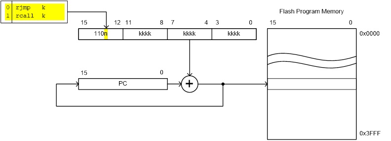
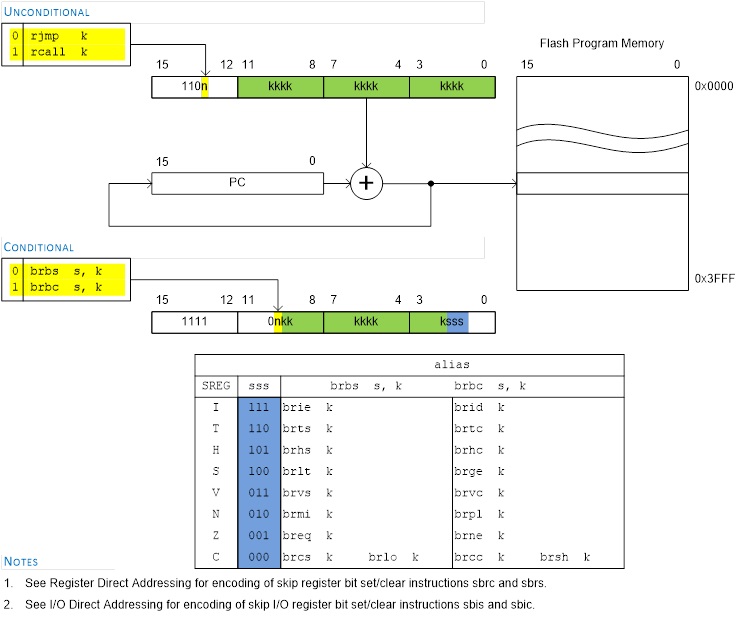
- Jump relative to PC + (
, where k = 12)
PC-2048 to PC+2047, within 16 K word address space of ATmega328P
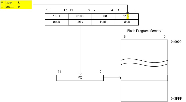
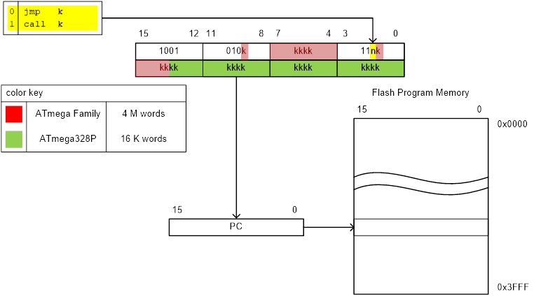
HOW THE DIRECT UNCONDITIONAL CONTROL TRANSFER INSTRUCTIONS JMP AND CALL WORK
- From a computer engineer’s perspective, a direct jump is accomplished by loading the target address into the program counter (PC). In the example, the target address is equated to label “loop.”
- To provide a more concrete example, assume the label loop corresponds to address 0x0123 in Flash Program Memory.
- To execute this instruction, the control logic of central procession unit (CPU) loads the 16-bit Program Counter (PC) register with 0x123.
- Consequently, on the next fetch cycle it is the instruction at location 0x0123 that is fetched and then executed. Control of the program has been transferred to this address.
HOW THE RELATIVE UNCONDITIONAL CONTROL TRANSFER INSTRUCTIONS RJMP AND RCALL WORK
- From a computer engineer’s perspective, a relative jump is accomplished by adding a 12-bit signed offset to the program counter (PC) . The result corresponding to the target address. In the example, the target address is equated to label “loop.”
- To provide a more concrete example, assume the label loop corresponds to address 0x0123 in Flash Program Memory (the target address).
- An rjmp loop instruction is located at address 0x206. When the rjmp is executed, the PC is currently fetching what it thinks is the next instruction to be executed at address 0x207.
- To accomplish this jump the relative address (kkkk kkkk kkkk) is equal to 0xF1C (i.e., 0x123 – 0x207).
- Consequently, on the next fetch cycle it is the instruction at location 0x0123 that is fetched and then executed. Control of the program has been transferred to this address.
BRANCH INSTRUCTIONS
- When a conditional or branch instruction is executed one of two things may happen.
- If the test condition is true then the branch will be taken (see jump instructions).
- If the test condition is false then nothing happens (see nop instruction).
Note: This statement is not entirely accurate. Because the program counter always points to the next instruction to be executed, during the execution state, doing nothing means fetching the next instruction.
- The “test condition” is a function of one SREG flag bit. For example, the branch if equal (breq) or not equal (brne) instructions test the Z flag.
HOW THE RELATIVE CONDITIONAL CONTROL TRANSFER INSTRUCTION BREQ WORKS
- If a relative branch is taken (test condition is true) a 7-bit signed offset is added to the PC. The result corresponding to the target address. In the example, the target address is equated to label “match.”
- To provide a more concrete example, assume the label nomatch corresponds to address 0x0123 in Flash Program Memory (the target address).
- A brne nomatch instruction is located at address 0x0112. When the brne instruction is executed, the PC is currently fetching what it thinks is the next instruction to be executed at address 0x0113.
- To accomplish this jump the relative address (kk kkkk) is equal to 0b01_0000 (i.e., 0x123 – 0x113).
- Consequently, on the next fetch cycle it is the instruction at location 0x0123 that is fetched and then executed. Control of the program has been transferred to this address.
BRANCH INSTRUCTIONS
- All conditional branch instructions may be implemented as brbs s,k or brbc s,k, where s is the bit number of the SREG flag bit. For example brbs 6, bitset would branch to label bitset, if the SREG T bit was set.
- To make your code more readable, the AVR assembler adds the following “alias” instructions.
- SREG Flag bit is clear (brFlagc) or set (brFlags) by name (I, T, H, S, V, N, Z, C) or bit (brbc, brbs).
- These SREG flag bits (I, T, H, S, V, N, Z, C) use more descriptive mnemonics.
- Branch if equal (breq) or not equal (brne) test the Z flag.
- Unsigned arithmetic branch if plus (brpl) or minus (brmi) test the N flag, while branch if same or higher (brsh) or lower (brlo), test the C flag and are equivalent to brcc and brcs respectively.
- Signed 2’s complement arithmetic branch if number is less than zero (brlt) or greater than or equal to zero (brge) test the S flag
Skip if …
- Bit (b) in a register is clear (sbrc) or set (sbrs).
- Bit (b) in I/O register is clear (sbic) or set (sbis). Limited to I/O addresses 0-31
Note:
- All branch instructions are relative to PC + (
, where k = 7) + 1
PC-64 to PC+63
- Skip instructions may take 1, 2, or 3 cycles depending if the skip is not taken, and the number of Flash program memory words in the instruction to be skipped (1 or 2).
CONDITIONAL BRANCH ENCODING
Here is how the brbs, brbc and their alias assembly instructions are encoded.
A CONDITIONAL CONTROL TRANSFER (BRANCH) SEQUENCE
A conditional control transfer (branch) sequence is typically comprised of two (2) instructions.
1. The first instruction performs some arithmetic or logic operation using the ALU of the processor.
- Examples of this first type of instruction includes: cp, cpc, cpi, tst
- These ALU operations result in SREG flag bits 5 to 0 being set or cleared (i.e., H, S, V, N, Z, C).
- To allow for multiple branch conditions to be tested, these instructions typically do not modify any of our 32 general purpose registers.
- The compare instructions cp, cpc, cpi should be used when you want to understand the relationship between two registers. For compare instructions, this is accomplished by performing a subtraction operation without a destination operand (cp r16,r17 is equivalent to r16 – r17).
- The tst instruction should be used when you want to test if the number in one register is negative or zero. For a test instruction, this is accomplished by performing an and operation with the destination and source registers being the same (tst r16 is equivalent to and r16,r16).
WARNING: The Atmel “Instruction Set Summary” document incorrectly classifies compare instructions (cp, cpc, cpi) as “Branch Instructions.” They should be listed under “Arithmetic and Logical Instructions.” To highlight this inconsistency on Atmel’s part, the tst instruction is correctly listed under “Arithmetic and Logical Instructions.”
2. The second instruction is a conditional branch instruction testing one or more SREG flag bits.
CONDITIONAL BRANCH INSTRUCTION SUMMARY
As mentioned in the previous slide, typically a conditional control transfer instruction follows a compare or test instruction, where some relationship between two registers is being studied. The following table may be used to quickly find the correct conditional branch instructions for these conditions.
A Conditional Control Transfer (Branch) Example
Here is how a high-level language decision diamond would be implemented in assembly.
; directions (see note)
.EQU south=0b00 ; most significant 6 bits zero
.EQU east=0b01
.EQU west=0b10
.EQU north=0b11
cpi r16,north ; step 1: Z flag set if r16 = 0b00000011
breq yes ; step 2: branch if Z flag is set
Note: These equates are included in testbench.inc
IMPLEMENTING A HIGH-LEVEL IF STATEMENT
- A high-level if statement is typically comprised of…
- Conditional control transfer sequence (last slide) where the complement (not) of the high-level conditional expression is implemented.
- High-level procedural block of code is converted to assembly.
- C++ High-level IF Expression
if (r16 == north) {
block of code to be executed if answer is yes.
} - Assembly Version
cpi r16,north ; Is bear facing north?
brne no ; branch if Z flag is clear (not equal)
block of code to be executed if answer is yes.
no:
IMPLEMENTING A HIGH-LEVEL IF…ELSE STATEMENT
- A high-level if…else statement is typically comprised of…
- Conditional control transfer sequence where the complement (not) of the high-level conditional expression is implemented.
- High-level procedural block of code for yes (true) condition.
- Unconditional jump over the no (false) block of code.
- High-level procedural block of code for no (false) condition.
- C++ High-level if…else Expression
if (r16 == north) {
block of code to be executed if answer is yes (true).
}
else {
block of code to be executed if answer is no (false).
} - Assembly Version
cpi r16,north ; Is bear facing north?
brne else ; branch if Z flag is clear (not equal)
block of code to be executed if answer is yes.
rjmp end_if
else:
block of code to be executed if answer is no.
end_if:
ASSEMBLY OPTIMIZATION OF A HIGH-LEVEL IF…ELSE STATEMENT – ADVANCED TOPIC –
- If the if-else blocks of code can be done in a single line of assembly then the program flow is modified to guess the most likely outcome of the test.
- This is possible if the value of a variable (for example the segments of a 7-segment display to be turned on) is the only thing done in each block.
- This optimized program flow will always execute as fast as the normal if..else program flow (if the guess if wrong) and faster if the guess is correct.
- This implementation is also more compact and often easier to understand.
- Assembly Version

; 7-segment display (see note)
.EQU seg_a=0
.EQU seg_b=1
.EQU seg_c=2
…
ldi r17,1<
cpi r16, north ; Is bear facing north?
breq done
clear (not equal)
block of code to be executed if guess was wrong.
done:
Note: These equates are included in spi_shield.inc
Program Examples: Group A or B – Pseudocode example
- Objective
Assign the least significant 4 switches on the CSULB shield to group A and the most significant to group B. Based on user input, display A or B based on which group has the higher value. In the event of a tie display E for equal. For this programming problem assume that people choose A 50% of the time, B 40% of the time, and set the switches equal to each other 10% of the time.
- Pseudocode

- Using the ReadSwitches subroutine or reading the I/O ports directly, input group A into register A (.DEF regA = r16) and group B into register B (.DEF regB = r17)
- Preload the output register (.DEF answer = r18) with the letter A
Guess
- If (A>B) then go to display answer.
- Preload the output register with the letter B
Guess
- If (B>A) then go to display answer.
- Set answer to E and display answer.
- Seven segment display values.

- Programming work around by interchanging Rd and Rr.

Direction Finder – Two Program Solutions
- Objective
Design a digital circuit with two (2) switches that will turn on one of the rooms 4 LED segments indicating the direction you want your bear to walk
Direction Finder – Truth Table Implementation
 lds r16, dir // move direction bits into a working register

 // facing east (segment b)
 bst r16,0   // store direction bit 0 into T
 bld var_B,0 // load r16 bit 0 from T
 bst r16,1   // store direction bit 1 into T
 bld var_A,0 // load r17 bit 0 from T
 com var_A   // B = /A * B
 and var_B, var_A
 bst var_B,0 // store r16 bit 0 into T
 bld spi7SEG, seg_b // load r8 bit 1 from T

Implementation of Boolean expressions for segments a, f, and g (circuit schematic)
Direction Finder – Using Conditional Expressions
lds r16, dir
ldi r17, 1< cpi r16,south ; if bear is facing south then we are done
breq done
ldi r17, 1< cpi r16,west ; if bear is facing west then we are done
breq done
ldi r17, 1< cpi r16,east ; if bear is facing east then we are done
breq done
ldi r17, 1<
done:
mov spi7SEG, r17 ; answer to 7-segment register
call WriteDisplay
Pseudo-Instructions TurnLeft, TurnRight, and TurnAround
Using switches 3 and 2, located on Port C pins 3 and 2 respectively, input an action you want the bear to take. The three possible actions are do nothing, turnLeft, turnRight, and turnAround. Write a subroutine named WhichWay to take the correct action as defined by the following table.
; ————————–
; — Which Way Do I Go? —
call ReadSwitches // input port C pins (0x06) into register r7
bst switch, 3 // store switch bit 3 into T
brts cond_1X // branch if T is set
bst switch, 2 // store switch bit 2 into T
brts cond_01 // branch if T is set
cond_00:
rjmp whichEnd
cond_01:
rcall TurnRight
rjmp whichEnd
cond_1X:
// branch based on the state of switch bit 2
:
cond_10:
:
cond_11:
:
whichEnd:
Warning: The above code is for illustrative purposes only and would typically be found in the main looping section of code not in a subroutine. Do not use this code to implement your lab.
InForest and Implementation of IF…ELSE Expression
- The inForest subroutine tells us if the bear is in the forest (i.e., has found his way out of the maze).
- The rows and columns of the maze are numbered from 0 to 19 (13h) starting in the upper left hand corner.
- When the bear has found his way out of the maze he is in row minus one (-1). The subroutine is to return true (r25:r24 != 0) if the bear is in the forest and false (r25:r24 == 0) otherwise.
- The register pair r25:r24 is where C++ looks for return values for the BYTE data type.
InForest and Implementation of IF…ELSE Expression – Continued –
; ————————–
; ——- In Forest ——–
; Called from whichWay subroutine
; Input: row Outputs: C++ return register (r24)
; No others registers or flags are modified by this subroutine
inForest:
push reg_F // push any flags or registers modified
in reg_F,SREG
push r16
lds r16,row
test if bear is in the forest
endForest:
clr r25 // zero extend
pop r16 // pop any flags or registers placed on the stack
out SREG,reg_F
pop reg_F
ret
Appendix
APPENDIX A: CONTROL TRANSFER INSTRUCTION ENCODING
Direct
All control transfer addressing modes modify the program counter.
CONTROL TRANSFER INSTRUCTION ENCODING – Indirect
CONTROL TRANSFER INSTRUCTION ENCODING – Relative
APPENDIX B – AVR STATUS REGISTER (SREG)
Non ALU
- Bit 7 – I: Global Interrupt Enable
The Global Interrupt Enable bit must be set for the interrupts to be enabled. The individual interrupt enable control is then performed in separate control registers. The I-bit is cleared by hardware after an interrupt has occurred, and is set by the reti instruction. The I-bit can also be set and cleared by the application with the sei and cli instructions. - Bit 6 – T: Bit Copy Storage
The Bit Copy instructions bld (Bit LoaD) and bst (Bit STore) use the T-bit as source or destination. A bit from a register can be copied into T (RbT) by the bst instruction, and a bit in T can be copied into a bit in a register (T
Rb) by the bld instruction.
ALU
Signed two’s complement arithmetic
- Bit 4 – S: Sign Bit, S = N ⊕ V
Bit set if answer is negative with no errors or if both numbers were negative and error occurred, zero otherwise. - Bit 3 – V: Two’s Complement Overflow Flag
Bit set if error occurred as the result of an arithmetic operation, zero otherwise. - Bit 2 – N: Negative Flag
Bit set if result is negative, zero otherwise.
Unsigned arithmetic
- Bit 5 – H: Half Carry Flag
Carry from least significant nibble to most significant nibble. Half Carry is useful in BCD arithmetic. - Bit 0 – C: Carry Flag
The Carry Flag C indicates a carry in an arithmetic operation. Bit set if error occurred as the result of an unsigned arithmetic operation, zero otherwise.
Arithmetic and Logical
- Bit 1 – Z: Zero Flag
The Zero Flag Z indicates a zero result in an arithmetic or logic operation.
APPENDIX C – CONTROL TRANSFER (BRANCH) INSTRUCTIONS
Compare and Test cp, cpc, cpi, tst, bst
Unconditional
- Relative (1) rjmp, rcall
- Direct jmp, call
- Indirect ijmp, icall
- Subr. & Inter. Return ret, reti
Conditional
- Branch if (2) …
- SREG Flag bit is clear (brFlagc) or set (brFlags) by name (I, T, H, S, V, N, Z, C) or bit (brbc, brbs).
- These SREG flag bits (I, T, H, S, V, N, Z, C) use more descriptive mnemonics.
- Branch if equal (breq) or not equal (brne) test the Z flag.
- Unsigned arithmetic branch if plus (brpl) or minus (brmi) test the N flag, while branch if same or higher (brsh) or lower (brlo), test the C flag and are equivalent to brcc and brcs respectively.
- Signed 2’s complement arithmetic branch if number is less than zero (brlt) or greater than or equal to zero (brge) test the S flag
- Skip if …
- Bit (b) in a register is clear (sbrc) or set (sbrs).
- Bit (b) in I/O register is clear (sbic) or set (sbis). Limited to I/O addresses 0-31
Note:
- Branch relative to PC + (
, where k = 12) + 1
PC-2047 to PC+2048, within 16 K word address space of ATmega328P
- All branch relative to PC + (
, where k = 7) + 1
PC-64 to PC+63, within 16 K word address space of ATmega328P
APPENDIX D – ATMEGA328P INSTRUCTION SET
AVR Control Transfer: Looping
READING
The AVR Microcontroller and Embedded Systems using Assembly and C
by Muhammad Ali Mazidi, Sarmad Naimi, and Sepehr Naimi
Sections: 3.1, 3.3
ADDITIONAL READING
Introduction to AVR assembler programming for beginners, controlling sequential execution of the program http://www.avr-asm-tutorial.net/avr_en/beginner/JUMP.html
AVR Assembler User Guide
Table of Contents
LOOP CONSTRUCTS IN C++ AND ASSEMBLY
Loop Example 1: Loop through a block of code 7 times.
- Typically we increment the counter variable in C++.
for(int i=0; i<7; i++); // This statement loops 7 times {i: 0,1,2,3,4,5,6}
- As shown in the example at the right below, in assembly we decrement the counter variable.
{i: 7,6,5,4,3,2,1}
This allows us to immediately test the SREG Z-flag bit without an intermediate compare instruction.
| C++ | Assembly | |
| for(int i=7; i>0; i—-) { Block of code }
|
int i = 7; do { Block of code i—-; } while(i>0);
|
ldi r16, 7 loop: Block of code
|
BUTTON DEBOUNCE EXAMPLE
- In the screen capture (red waveform), a button bounces for about 400us when pressed. Once the transition is detected, we want to design a software loop that will do nothing while the switch input stabilizes.
- Specifically, we want to design a software delay routine that will generate a delay of approx.
.
DELAY CALCULATION FOR AVR
We begin by designing a simple loop.
wait:
ldi r16, ____ // Loop Count
delay:
dec r16 // ____ machine cycles
brne delay // ____ machine cycles
To discover the delay generated by our “software” loop we begin by finding the answers to the questions.
- What “Loop Count” Lcnt will generate the maximum delay?
- What is a machine cycle and how many machine cycles are required for each line of code?
- What is the number of machine cycles Nmc in 1 loop?
INSTRUCTION (OR MACHINE) CYCLE TIME FOR THE AVR
- Machine Cycle – The number of clock cycles it takes the CPU to fetch and execute an instruction.
- Because the AVR processors incorporate a 2-stage pipeline, there is a one-to-one relationship between an AVR machine cycle and a clock cycle. In contrast for the non-pipelined 8051 microcontroller one machine cycle = 12 clock cycles.
- Therefore to calculate the time it takes for one machine cycle you only need to take the inverse of the clock frequency.
| Example: |
- As shown in the “Complete Instruction Set Summary” on page 427 of the AVR Instruction Set Document (Atmel doc0856) most AVR instructions need only one or two clock cycles to fetch and execute an instruction.

- Given a clock frequency of 16 MHz and based on the above table a multiple MUL instruction will take
to execute
PIPELINING
Before you can fully understand branching and looping you need to understand the concept of pipelining and how it is implemented in our AVR processor.
- Pipelining is a technique that breaks operations, such as instruction processing (fetch and execute) into smaller distinct stages so that a subsequent operation can begin before the previous one has completed.
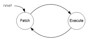
- For most instructions, especially one based on a modified Harvard memory model, program memory is not accessed during the execution cycle. This memory down time could be used to fetch the next instruction to be executed, in parallel with the execution cycle of the current instruction. Here then is an opportunity for pipelining!
AVR INTERSTAGE PIPELINE REGISTERS
- A pipeline stage begins and ends with a register; controlled by a clock. Technically these are known as interstage pipeline registers.
- With respect to our AVR architecture the two registers of interest are the Program Counter (PC) and the Instruction Register (IR).
- Between the register(s) is combinational logic. Although counter-intuitive, Flash Program memory can be viewed as combinational logic with an address generating a word of data.
- Without pipelining these two registers in the control unit (PC, IR) would require two clock cycles to complete a basic computer operation cycle. Specifically, an instruction is (1) fetched and then (2) executed.
AVR TWO-STAGE INSTRUCTION PIPELINE
- The AVR pipeline has two independent stages. The first stage fetches an instruction and places it in the Instruction Register (IR), while the second stage is executing the instruction.
- For our RISC architecture most instructions are executed in a single cycle (also known as elemental instructions). In this perfect world where all instructions take one cycle to fetch and one cycle to execute, after an initial delay of one cycle to fill the pipeline, known as latency, each instruction will take only one cycle to complete.
BRANCH PENALTY
- Within the context of pipeline architecture, when the execution stage of the pipeline is executing a conditional branch instruction, the execution stage must “predict” the outcome of the instruction in order to fetch what it “guesses” will be the next instruction.
- While on average 80% of the time a branch is taken, the AVR always guesses that the branch will not be taken. This guess is made simply because it is the simplest to implement (the program counter automatically points at the next instruction to be executed).
- When a branch is taken, and the guess is wrong, the processor must build the pipeline from scratch thus accruing a “penalty.” With our simple 2-stage pipeline that penalty is one clock cycle as shown in the AVR Instruction Set Document.

BUTTON DEBOUNCE EXAMPLE – CONTINUED
In the screen capture (red waveform), a button bounces for about 400us when pressed. Once the transition is detected, we want to design a software loop that will do nothing while the switch input stabilizes. To remove the noise, we will design a software delay routine that will generate a delay of approx. 500 us.
DELAY CALCULATION FOR AVR
- Returning to our simple software loop
wait:
ldi r16, ____ // Loop Count
delay:
dec r16 // 1 clock cycle
brne delay // + 2 cycles if true, 1 cycle if false
= Delay generated by the loop
= period of one machine cycle =
(note: 1 machine cycle = 1 clock cycle) = 1 / 16 MHz = 0.0625 usec
= number of machine cycles in 1 loop = 3 (for brne Nmc = 2 cycles, we subtract 1 for the one cases where our guess is correct.)
= number of times loop is run (Loop Count) = ?
CALCULATING MAXIMUM DELAY
- Next we will calculate the maximum delay
= 0 which results in a count of 256
(approx) Note: the -1 is subtracting the one true result
- Now Let’s increase this delay by adding a nop instruction and then recalculating the maximum delay
= number of machine cycles in 1 loop = 4
wait:
clr r16 // 0 = maximum delay
delay:
nop // 1
dec r16 // 1 clock cycle
brne delay // + 2 cycles if true, 1 cycle if false
(approx) with r16 = 0 (clr r16)
CALCULATING LOOP COUNT FOR A GIVEN DELAY
- To generate a delay of 500 µs we will initialize r16 for a delay of 50 µs and then write an outside loop that will run the inside loop 10 times for a total delay of approximately 500 µs
- Solving our Tmax equation for Loop Count Lcnt
- Set Lcnt for a delay of 50 µsec
wait:
ldi r16, 0xC8 // 200
delay:
nop // 1
dec r16 // 1 clock cycle
brne delay // + 2 cycles if true, 1 cycle if false
LOOP INSIDE A LOOP DELAY
On your own, create an outside loop with a count of 10 to give us a delay of approximately 500 µsec (Hint see Example 3-18 in your textbook)
DESIGN EXAMPLE WITH EE346 SHIELD
When the user presses the button, read first 3 switches (least significant), if the number is less than or equal to 5 then calculate factorial. If greater than 5 turn on decimal point. Display the least significant 4 bits of the answer.
MY DESIGN STEPS
Step 1: Initialized Ports
Step 2: Turned on LED 0 to indicate initialization complete
Step 3: Wrote code to pulse the clock
Step 4: Read in pin waiting for button to be pressed (Loop Example 1)
Step 5: Need to filter out Bounce (Loop Example 2)
Maximum delay that could be generated was only 48 usec
Step 6: Added a NOP instruction, max delay was now 64 usec
Set delay for nice even number of 50 usec
Step 7: Made an outside loop of 10 (Loop Example 3)
Step 8: Converted loop to a subroutine so I could change condition to button release.
Step 9: Check for button pressed and then released
Step 10: Read Switch and check if less than or equal to 6
Step 11: Calculate Factorial (Loop Example 4)
Step 12: Store 4 digit answer to SRAM (SRAM Indirect Addressing Mode)
Step 13: Sequentially, Load each digit and … (SRAM Indirect Addressing Mode)
Step 14: convert to 7-segment display (Flash Program Indirect Addressing Mode)
CSULB PROTO-SHIELD SCHEMATIC
CONFIGURE GPIO PORTS
ATMEGA328P INSTRUCTION SET
AVR Subroutine Basics
READING
The AVR Microcontroller and Embedded Systems using Assembly and C
by Muhammad Ali Mazidi, Sarmad Naimi, and Sepehr Naimi
Chapter 3, pages 118 to 125
Table of Contents
AVR Subroutine Basics
- How do I go to and return from a subroutine?
rcall label
call label
icall label
ret
- AVR Call Addressing Modes
Relative The relative address is encoded in the machine instruction using 12 bits. Assuming that the Program Counter (PC) is pointing at the next instruction to be executed, a relative call can jump within a range of -2n-1 to 2n-1 – 1 program words, in other words -2K ≤ PC < 2K – 1. n = 12 bits, K = 210 = 1024, and a program word is 16-bits. Long full 16 K word (32K byte) address space Indirect full 16 K word (32K byte) address space
- Why Subroutines?
- My Little Subroutine Dictionary
- Assembly Subroutine Template
- How to Send Information to and/or from the Calling Program
- Rules for Working with Subroutines
WHY SUBROUTINES?
- Divide and Conquer – Allow you to focus on one small “chunk” of the problem at a time.
- Code Organization – Gives the code organization and structure. A small step into the world of object-oriented programming.
- Modular and Hierarchical Design – Moves information about the program at the appropriate level of detail.
- Code Readability – Allows others to read and understand the program in digestible “bites” instead of all at once. Higher level subroutines with many lower level subroutine calls take on the appearance of a high level language.
- Encapsulation – Insulates the rest of the program from changes made within a procedure.
- Team Development – Helps multiple programmers to work on the program in parallel; a first step to configuration control. Allows a programmer to continue writing his code, independent of other team members by introducing “stub” subroutines. A stub subroutine may be as simple as the subroutine label followed by a return instruction.
MY LITTLE SUBROUTINE DICTIONARY
SUBROUTINE VERSUS FUNCTION
- Functions and subroutines are the most basic building block you can use to organize your code.
- Functions are very similar to subroutines; their syntax is nearly identical, and they can both perform the same actions. However, Functions return a value to the code that called it.
- For this course the terms Subroutine, Procedure and Method may describe a Subroutine or Function based on context.
PARAMETER VERSUS ARGUMENT
- In everyday usage, “parameter” and “argument” are used interchangeably to refer to the things that you use to define and call methods or functions.
- Often this interchangeability doesn’t cause ambiguity. It should be noted, though, that conventionally, they refer to different things.
- A “parameter” is the thing used to define a method or function while an “argument” is the thing you use to call a method or function.

- Ultimately, it doesn’t really matter what you say. People will understand from the context.
ASSEMBLY SUBROUTINE TEMPLATE
; —- My Subroutine ——-
; Called from Somewhere
; Input: Registers, SRAM variables, or I/O registers
; Outputs: None for a subroutine or r25:r24 register pair for a C function
; No others registers or flags are modified by this subroutine
; ————————–
MySubroutine:
push r15 // push any flags or registers modified by the procedure
in r15,SREG
push r16
my assembly code
endMySubroutine:
clr r25 // zero-extended to 16-bits for C++ call (optional)
pop r16 // pop any flags or registers placed on the stack
out SREG,r15
pop r15
ret
HOW TO SEND INFORMATION TO AND/OR FROM THE CALLING PROGRAM
There are many way to send information to and from a subroutine or function. Here are a few…
- In Register(s) or Register Pair(s) agreed upon between the calling program and Procedure or Function.
- By setting or clearing one of the bits in SREG (I, T, H, S, V, N, Z, C).
- In an SRAM variable, this method is not recommended.
- As part of a Stack Frame, this method is beyond the scope of a course on microcontrollers but is highly recommended.
HOW TO SEND INFORMATION TO AND/OR FROM YOUR C PROGRAM
When working in a Mixed C and Assembly programming environment, our subroutines and functions communicate using Register Pairs.
- Mixed C and Assembly parameter passing Register Pairs
In your C Program…
// C Assembly External Declarations
extern void mySubr(uint8_t param1, uint16_t param2, uint16_t param3);
extern uint8_t myFunc(uint8_t param1, uint16_t param2, uint16_t param3);
In your Assembly Program…
; Define Assembly Directives
.DEF parm1H = r25
.DEF parm1L = r24
.DEF parm2H = r23
.DEF parm2L = r22
.DEF parm3H = r21
.DEF parm3L = r20
mySubr:
Assembly Code
ret
- 8-bit return values (uint8_t data type) are zero/sign-extended to 16-bits in r25:r24 by called function.
RULES FOR WORKING WITH SUBROUTINES
Here are a few rules to remember when writing your main program and subroutines.
- Always disable interrupts and initialize the stack pointer at the beginning of your program.
; Disable interrupts and configure stack pointer for 328P
cli
ldi r16,low(RAMEND) // RAMEND address 0x08ff
out SPL,r16 // Stack Pointer Low SPL at i/o address 0x3d
ldi r16,high(RAMEND)
out SPH,r16 // Stack Pointer High SPH at i/o address 0x3e - Always initialize variables and registers at the beginning of your program. Do not re-initialize I/O registers used to configure the GPIO ports or other subsystems within a loop or a subroutine. For example, you only need to configure the port pins assigned to the switches as inputs with pull-up resistors once.
- Push (push r7) any registers modified by the subroutine at the beginning of the subroutine and pop (pop r7) in reverse order the registers at the end of the subroutine. This rule does not apply if you are using one of the registers or SREG flags to return a value to the calling program. Comments should clearly identify which registers are modified by the subroutine.
- You cannot save the Status Register SREG directly onto the stack. Instead, first push one of the 32 registers on the stack and then save SREG in this register. Reverse the sequence at the end of the subroutine.
push r15
in r15, SREG
:
out SREG, r15
pop r15 - Never jump into a subroutine. Use a call instruction (rcall, call) to start executing code at the beginning of a subroutine.
- Never jump out of a subroutine. Your subroutine should contain a single return (ret) instruction as the last instruction (ret = last instruction).
- You do not need an .ORG assembly directive. As long as the previous code segment ends correctly (rjmp, ret, reti) your subroutine can start at the next address.
- You do not need to clear a register or any variable for that matter before you write to it.
clr r16; this line is not required
lds r16, A - All blocks of code within the subroutine or Interrupt Service Routine (ISR) should exit the subroutine through the pop instructions and the return (ret, reti).
- It is a good programming practice to include only one return instruction (ret, reti) located at the end of the subroutine.
- Once again, never jump into or out of a subroutine from the main program, an interrupt service routine, or any other subroutine. However, subroutines or ISRs may call (rcall) other subroutines.
BASIC STRUCTURE OF A SUBROUTINE – A REVIEW
- Load argument(s) into input registers (parameters) as specified in the header of the subroutine (typically r24, r22).
- Call the Subroutine
- Save an image of the calling programs CPU state by pushing all registers modified by the subroutine, including saving SREG to a register.
- Do something with the return value(s) stored in the output register(s) specified in the header of the subroutine (typically r24, r22).
- Restore image of the calling programs CPU state by popping all registers modified by the subroutine, including loading SREG from a register.
- Return
AVR Peripherals: General-Purpose Input/Output
READING
The AVR Microcontroller and Embedded Systems using Assembly and C
by Muhammad Ali Mazidi, Sarmad Naimi, and Sepehr Naimi
Sections: 4.1, 4.2, 6.4
SOURCE MATERIAL
1. ATmega328P Datasheet Section 13 “I/O-Ports” http://www.atmel.com/dyn/resources/prod_documents/doc8161.pdf
2. Arduino Port Registers
3. arduino-duemilanove-schematic
4. arduino-proto-shield
Table of Contents
Source: ATmega328P Data Sheet http://www.atmel.com/dyn/resources/prod_documents/8161S.pdf page 5 ******
ATMEGA GENERAL PURPOSE DIGITAL I/O PORTS
- The ATmega328P has 23 General Purpose Digital I/O Pins assigned to 3 GPIO Ports (8-bit Ports B, D and 7-bit Port C)
- Each I/O port pin may be configured as an output with symmetrical drive characteristics. Each pin driver is strong enough (20 mA) to drive LED displays directly.
- Each I/O port pin may be configured as an input with or without a pull-up resistors. The values for the pull up resistors can range from 20 – 50 K ohms.
- Each I/O pin has clamping diodes to protect input circuit from undervoltage/overvoltage and ESD conditions.
DUAL ROLE OF PORTS B, C AND D OF THE ATMEGA328P
I/O Ports B (PB7:0), Port C (PC5:0), and Port D (PD7:0)
Ports B, C, and D are bi-directional I/O ports with internal pull-up resistors (selected for each bit). The Port output buffers have symmetrical drive characteristics with both high sink and source capability.
Interrupts (INT1, INT0, PCINT23..0)
External Interrupts are triggered by the INT0 and INT1 pins or any of the PCINT23..0 pins. Observe that, if enabled, the interrupts will trigger even if the INT0 and INT1 or PCINT23..0 pins are configured as outputs. This feature provides a way of generating a software interrupt.
AVCC
AVCC is the supply voltage pin for the A/D Converter. It should be externally connected to VCC. If the ADC is used, it should be connected to VCC through a low-pass filter.
AREF
AREF is the analog reference pin for the A/D Converter.
ADC5:0
These pins serve as analog inputs to the A/D converter. These pins are powered from the analog supply and serve as 10-bit ADC channels.
I/O PORT PIN AS AN OUTPUT
- To configure a Port (x) pin as an output set corresponding bit (n) in the Data Direction Register (DDxn) to 1. Once configured as an output pin, you control the state of the pin (1 or 0) by writing to the corresponding bit (n) of the PORTxn register.
- Writing (signal WPx) a logic one to PINxn toggles the value of PORTxn, independent on the value of DDxn. Note that the SBI instruction can be used to toggle one single bit in a port.
I/O PORT PIN AS AN INPUT
- To configure a Port (x) pin as an input set corresponding bit (n) in the Data Direction Register (DDxn) to 0. To add a pull-up resistor set the corresponding bit (n) of the PORTxn register to 1 (see illustration).
- You can now read the state of the input pin by reading the corresponding bit (n) of the PINxn register.
ACCESSING GPIO LINES IN ASSEMBLY
DESIGN EXAMPLE 1 – Read Switches
Problem: Program GPIO Port C bits 5 to 0 as inputs with pull-up resistors. Read GPIO Port C into register r6 and move bit 4 to register r7 bit 0. Your program should not modify Port C bits 7 and 6.
; Initialize Switches with Pull-up resistors
in r16, DDRC // Port C DDR for switches 5 to 0
cbr r16,0b00111111 // define bits 5 to 0 as input (clear)
out DDRC,r16 // output DDxn = 0 PORTxn = Undefined
in r16,PORTC // PORT C Register for switches 5 to 0
sbr r16,0b00111111 // add pull-up resistors (PUR)
out PORTC,r16 // output DDxn = 0 PORTxn = 1
Main:
:
in r6,PINC // R6 <- IO[0x06]
bst r6,4 // T <- R6 bit 4
bld r7,0 // R7 bit 0 (seg_a) <- T
DESIGN EXAMPLE 2 – CONFIGURE D FLIP-FLOP
Problem: Program GPIO Port D bit 5 as an output and bit 2 as an input without a pull-up resistor.
; Pushbutton debounce port D pins
.EQU dff_clk=PORTD5 // clock of debounce flip-flop
.EQU dff_Q=PIND2 // Q output of debounce flip-flop
; initialize push-button debounce circuit
sbi DDRD,dff_clk // flip-flop clock, DDRD5 = 1; PORTD5 = Undefined
cbi PORTD,dff_clk // DDRD5 = 1; PORTD5 = 0
cbi DDRD,dff_Q // flip-flop Q DDRD2 = 0; PORTD2 = Undefined
cbi PORTD,dff_Q // flip-flop Q DDRD2 = 0; PORTD2 = 0
REGISTER SUMMARY AND THE I/O PORT
- Three I/O memory address locations are allocated for each port, one each for the Data Register – PORTx, Data Direction Register – DDRx, and the Port Input Pins – PINx.
- The Port Input Pins I/O location PINx is Read Only, while the Data Register and the Data Direction Register are read/write.
- However, Writing a logic one to a bit in the PINx Register, will result in a Toggle in the corresponding bit in the Data Register.
- In addition, the Pull-up Disable – PUD bit in MCUCR disables the pull-up function for all pins in all ports when set.
I/O PORT PIN SCHEMATIC
I/O PORT PIN CONFIGURATIONS
| Inputs | Outputs | |||
| DDRXn | PORTXn | I/O | Pull-Up | Comments |
| 0 | 0 | Input | No | Read “Synchronized” PINXn |
| 0 | 1 | Input | Yes | |
| 1 | X | Output | N/A | Write bit to PORTXn |
Appendix
APPENDIX A – PROGRAM I/O PORT AS AN INPUT USING MNEMONICS
.INCLUDE
; C:\Program Files\Atmel\AVR Tools\AvrAssembler2\Appnotes\m328Pdef.inc
in r16,DDRC // DDRC equated to 0x07 in m328Pdef.inc
cbr r16,(1<<pc5)|(1<<pc4)|(1<<pc3)|(1<<pc2)|(1<<pc1)|(1<<pc0)< span=””> out DDRC,r16 // output DDxn = 0; PORTxn = Undefined
in r16,PORTC // PortC equated to 0x08
sbr r16,(1<<pc5)|(1<<pc4)|(1<<pc3)|(1<<pc2)|(1<<pc1)|(1<<pc0)< span=””> out PORTC,r16 // output DDxn = 0; PORTxn = 1</pc5)|(1<<pc4)|(1<<pc3)|(1<<pc2)|(1<<pc1)|(1<<pc0)<></pc5)|(1<<pc4)|(1<<pc3)|(1<<pc2)|(1<<pc1)|(1<<pc0)<>
.INCLUDE “spi.inc”
The following Define and Equate Assembly Directives are defined in spi_shield.inc
.DEF spi7SEG=r8 // Text Substitution (copy-paste)
.DEF switch=r7
.EQU seg_a=0 // Numeric Substitution
in switch, PINC // R7 <- PINC
bst switch,4 // T <- R7 bit 4
bld spi7SEG,seg_a // R8 bit 0 <- T
Appendix B – I/O PORT PIN “SYNCHRONIZER”
- As previously discussed, you read a port pin by reading the corresponding PINxn Register bit. The PINxn Register bit and the preceding latch constitute a synchronizer. This is needed to avoid metastability if the physical pin changes value near the edge of the internal clock, but it also introduces a delay as shown in the timing diagram.
- Consider the clock period starting shortly after the first falling edge of the system clock. The latch is closed when the clock is low, and goes transparent when the clock is high, as indicated by the shaded region of the “SYNC LATCH” signal. The signal value is latched when the system clock goes low. It is clocked into the PINxn Register at the succeeding positive clock edge. As indicated by the two arrows tpd,max and tpd,min, a single signal transition on the pin will be delayed between ½ and 1½ system clock period depending upon the time of assertion.
Appendix C – SWITCHING BETWEEN I/O PORT PIN CONFIGURATIONS
- When switching between tri-state ({DDxn, PORTxn} = 0b00) and output high ({DDxn, PORTxn} = 0b11), an intermediate state with either pull-up enabled ({DDxn, PORTxn} = 0b01) or output low ({DDxn, PORTxn} = 0b10) must occur.
- Switching between input with pull-up ({DDxn, PORTxn} = 0b01) and output low ({DDxn, PORTxn} = 0b10) generates the same problem. You must use either the tri-state ({DDxn, PORTxn} = 0b00) or the output high state ({DDxn, PORTxn} = 0b11) as an intermediate step.
Interrupts and 16-bit Timer/Counter 1: ATmega328P Timing Subsystems
Reading
The AVR Microcontroller and Embedded Systems using Assembly and C
by Muhammad Ali Mazidi, Sarmad Naimi, and Sepehr Naimi
Sections: 9.1, 9.3
Table of Contents
ATmega328P Timing Subsystem
The ATmega328P is equipped with two 8-bit timer/counters and one 16-bit counter. These Timer/Counters let you…
- Turn on or turn off an external device at a programmed time.
- Generate a precision output signal (period, duty cycle, frequency). For example, generate a complex digital waveform with varying pulse width to control the speed of a DC motor
- Measure the characteristics (period, duty cycle, frequency) of an incoming digital signal
- Count external events
What is a Flip-Flop and a Counter
You can think of a D flip-flop as a one-bit memory. The something to remember on the D input of flip-flop is remembered on the positive edge of the clock input .
| Dt | Qt+1 |
| 0 | 0 |
| 1 | 1 |
| X | Qt |
The counter part of an ATmega328P Timer/Counter peripheral subsystem is an example of an asynchronous (ripple) counter, which is a collection of flip-flops with the clock input of stage n connected to the output of stage n -1
When compared with a synchronous counter, an asynchronous “ripple” counter: generates less noise and is less expensive. On the negative side, an asynchronous “ripple” counter is slower than a synchronous counter.
Timing Terminology
Frequency
The number of times a particular event repeats within a 1-s period. The unit of frequency is Hertz, or cycles per second. For example, a sinusoidal signal with a 60-Hz frequency means that a full cycle of a sinusoid signal repeats itself 60 times each second, or every 16.67 ms. For the digital waveform shown, the frequency is 2 Hz.
Period
The flip side of a frequency is a period. If an event occurs with a rate of 2 Hz, the period of that event is 500 ms. To find a period, given a frequency, or vice versa, we simply need to remember their inverse relationship, F = 1/T where F and T represent a frequency and the corresponding period, respectively.
Duty Cycle
In many applications, periodic pulses are used as control signals. A good example is the use of a periodic pulse to control a servo motor. To control the direction and sometimes the speed of a motor, a periodic pulse signal with a changing duty cycle over time is used.
Duty cycle is defined as the percentage of one period a signal is ON. The periodic pulse signal shown in the Figure is ON for 50% of the signal period and off for the rest of the period. Therefore, we call the signal in a periodic pulse signal with a 50% duty cycle. This special case is also called a square wave.
Timer 1 Modes of Operation
Normal Mode
- The simplest AVR Timer mode of operation is the Normal mode. Waveform Generation Mode for Timer/Counter 1 (WGM1) bits 3:0 = 0. These bits are located in Timer/Counter Control Registers A/B (TCCR1A and TCCR1B).
- In this mode the Timer/Counter 1 Register (TCNT1H:TCNT1L) counts up (incrementing), and no counter clear is performed. The counter simply overruns when it passes its maximum 16-bit value 0xFFFF and then restarts 0x0000.
- There are no special cases to consider in the Normal mode, a new counter value can be written anytime.
- In normal operation the Timer/Counter Overflow Flag (TOV1) bit located in the Timer/Counter1 Interrupt Flag Register (T1FR1) will be set in the same timer clock cycle as the Timer/Counter 1 Register (TCNT1H:TCNT1L) becomes zero. The TOV1 Flag in this case behaves like a 17th bit, except that it is only set, not cleared.
Timer/Counter 1 Prescalar
Timer/Counter 1 Normal Mode – Design Example
- In this design example, we want to write a 250 msec delay routine assuming a system clock frequency of 16.000 MHz and a prescale divisor of 64.
- The first step is to discover if our 16-bit Timer/Counter 1 can generate a 250 ms delay.
Variable Definitions
tclk_T1 : period of clock input to Timer/Counter1
fclk : AVR system clock frequency
fTclk_I/O : AVR Timer clock input frequency to Timer/Counter Waveform Generator
How to Calculate Maximum Delay (Normal Mode)
- The largest time delay possible is achieved by setting both TCNT1H and TCNT1L to zero, which results in the overflow flag TOV1 flag being set after 216 = 65,536 tics of the Timer/Counter1 clock.
, given
then
and therefore
- Clearly, Timer 1 can generate a delay of 250 msec
- Our next step is to calculate the TCNT1 load value needed to generate a 250 ms delay.
How to Calculate Timer Load Value
Steps to Calculate to Timer Load Value (Normal Mode)
Problem
Generate a 250 msec delay assuming a clock frequency of 16 MHz and a prescale divisor of 64.
Solution
- Divide desired time delay by tclkT1 where tclkT1 = 64/fclkI/O = 64 / 16.000 MHz = 4 µsec/tic
250msec / 4 µs/tic = 62,500 tics
short-cut: TCNT1H = high(-62,500) and TCNT1L = low(-62,500) - Subtract 65,536 – step 1
65,536 – 62,500 = 3,036 - Convert step 2 to hexadecimal.
3,036 = 0x0BDC
For our example TCNT1H = 0x0B and TCNT1L = 0xDC - Check Answer
3,036 tics x 4 µs/tic = 12.14 msec
262.14 msec – 250 msec = 12.14 msec √
Steps to Calculate Clock Divisor (Normal Mode)
In the previous example we assumed a divisor of 64, and then by calculating the maximum delay TMAX verified that this assumption was correct. After that we simply followed the steps defined in the previous slide to calculate the value to be loaded into 16-bit timer/counter TCNT1.
Where:
TMAX = maximum delay
N = divisor
n = number of flip-flops making-up the timer
fclk = system clock frequency
But what if we are not given N and need to find TCNT1 for a given delay tdelay. In this case we know that tdelay ≤ TMAX and applying a little algebra can find an equation for N.
Let’s take a second look at our 250 msec delay problem. This time we will not assume a divisor of 64. Applying equation 2 we have:
From Table 13.5 “Clock Select Bit Description” on page 10, we see that the possible clock divisors are 1, 8, 64, 256, and 1024. From this list we want to select the divisor that is the closest value, yet greater than or equal to N. For our example, not surprisingly the answer is again 64.
Polling Example – Assembly Version
; --------------------------
; ------ Delay 250ms ------
; Called from main program
; Input: none Output: none
; no registers are modified by this subroutine
Delay:
  push r15
  in   r15, SREG
  push r16
wait:
  sbis TIFR1, TOV1
  rjmp wait
  sbi TIFR1, TOV1 // clear flag bit by writing a one (1)
  ldi r16,0x0B    // load value high byte 0x0B
  sts TCNT1H,r16
  ldi r16,0xDC    // load value low byte 0xDC
  sts TCNT1L,r16
  pop r16
  out SREG, r15
  pop r15
  ret
Polling Example – C Version
; --------------------------
; ------ Delay 250ms ------
; Called from main program
; Input: none Output: none
void T1Delay()
{
  while (!(TIFR & (1<<tov1)))
  // eq. to Ex: 9-42 expression
  TIFR = 1<<tov1; clear="" timer="" overflow="" flag<br="">
  TCNT1H = 0x0B;
  TCNT1L = 0xDC;</tov1;></tov1)))
}
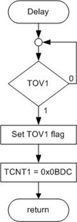
More Looping Examples
Here are six (6) other ways of implementing the looping part of the Polling Example written in assembly. See if you can come up with a few more.
| wait:
sbis TIFR1, TOV1 // targets a specific bit |
wait:
in r16, TIFR1 |
| wait:
in r16, TIFR1 |
|
| wait:
in r16, TIFR1 |
wait:
in r16, TIFR1 |
| wait:
in r16, TIFR1 |
wait:
in r16, TIFR1 |
Interrupts and 16-bit Timer/Counter 1: ATmega Interrupts
READING
The AVR Microcontroller and Embedded Systems using Assembly and C
by Muhammad Ali Mazidi, Sarmad Naimi, and Sepehr Naimi
Sections: 10.1, 10.4
Table of Contents
Interrupt Basics
- A microcontroller normally executes instructions in an orderly fetch-execute sequence as dictated by a user-written program.
- However, a microcontroller must also be ready to handle unscheduled, events that might occur inside or outside the microcontroller.
- The interrupt system onboard a microcontroller allows it to respond to these internally and externally generated events. By definition we do not know when these events will occur.
- When an interrupt event occurs, the microcontroller will normally complete the instruction it is currently executing and then transition program control to an Interrupt Service Routine (ISR). These ISR, which handles the interrupt.
- Once the ISR is complete, the microcontroller will resume processing where it left off before the interrupt event occurred.
The Main Reasons You Might Use Interrupts
- To detect pin changes (eg. rotary encoders, button presses)
- Watchdog timer (eg. if nothing happens after 8 seconds, interrupt me)
- Timer interrupts – used for comparing/overflowing timers
- SPI data transfers
- I2C data transfers
- USART data transfers
- ADC conversions (analog to digital)
- EEPROM ready for use
- Flash memory ready
ATmega328P Interrupt Vector Table
- The ATmega328P provides support for 25 different interrupt sources. These interrupts and the separate Reset Vector each have a separate program vector located at the lowest addresses in the Flash program memory space.
- The complete list of vectors is shown in Table 11-6 “Reset and Interrupt Vectors in ATMega328P. Each Interrupt Vector occupies two instruction words.
- The list also determines the priority levels of the different interrupts. The lower the address the higher is the priority level. RESET has the highest priority, and next is INT0 – the External Interrupt Request 0.
ATmega328P Interrupt Vector Table
| Vector No | Program Address | Source | Interrupt Definition | Arduino/C++ ISR() Macro Vector Name | Assembly Name |
|---|---|---|---|---|---|
| 1 | 0x0000 | RESET | Reset | ||
| 2 | 0x0002 | INT0 | External Interrupt Request 0 (pin D2) | (INT0_vect) | INT0addr |
| 3 | 0x0004 | INT1 | External Interrupt Request 1 (pin D3) | (INT1_vect) | INT1addr |
| 4 | 0x0006 | PCINT0 | Pin Change Interrupt Request 0 (pins D8 to D13) | (PCINT0_vect) | PCI0addr |
| 5 | 0x0008 | PCINT1 | Pin Change Interrupt Request 1 (pins A0 to A5) | (PCINT1_vect) | PCI1addr |
| 6 | 0x000A | PCINT2 | Pin Change Interrupt Request 2 (pins D0 to D7) | (PCINT2_vect) | PCI2addr |
| 7 | 0x000C | WDT | Watchdog Time-out Interrupt | (WDT_vect) | WDTaddr |
| 8 | 0x000E | TIMER2 COMPA | Timer/Counter2 Compare Match A | (TIMER2_COMPA_vect) | OC2Aaddr |
| 9 | 0x0010 | TIMER2 COMPB | Timer/Counter2 Compare Match B | (TIMER2_COMPB_vect) | OC2Baddr |
| 10 | 0x0012 | TIMER2 OVF | Timer/Counter2 Overflow | (TIMER2_OVF_vect) | OVF2addr |
| 11 | 0x0014 | TIMER1 CAPT | Timer/Counter1 Capture Event | (TIMER1_CAPT_vect) | ICP1addr |
| 12 | 0x0016 | TIMER1 COMPA | Timer/Counter1 Compare Match A | (TIMER1_COMPA_vect) | OC1Aaddr |
| 13 | 0x0018 | TIMER1 COMPB | Timer/Counter1 Compare Match B | (TIMER1_COMPB_vect) | OC1Baddr |
| 14 | 0x001A | TIMER1 OVF | Timer/Counter1 Overflow | (TIMER1_OVF_vect) | OVF1addr |
| 15 | 0x001C | TIMER0 COMPA | Timer/Counter0 Compare Match A | (TIMER0_COMPA_vect) | OC0Aaddr |
| 16 | 0x001E | TIMER0 COMPB | Timer/Counter0 Compare Match B | (TIMER0_COMPB_vect) | OC0Baddr |
| 17 | 0x0020 | TIMER0 OVF | Timer/Counter0 Overflow | (TIMER0_OVF_vect) | OVF0addr |
| 18 | 0x0022 | SPI, STC | SPI Serial Transfer Complete | (SPI_STC_vect) | SPIaddr |
| 19 | 0x0024 | USART, RX | USART, Rx Complete | (USART_RX_vect) | URXCaddr |
| 20 | 0x0026 | USART, UDRE | USART, Data Register Empty | (USART_UDRE_vect) | UDREaddr |
| 21 | 0x0028 | USART, TX | USART, Tx Complete | (USART_TX_vect) | UTXCaddr |
| 22 | 0x002A | ADC | ADC Conversion Complete | (ADC_vect) | ADCCaddr |
| 23 | 0x002C | EE READY | EEPROM Ready | (EE_READY_vect) | ERDYaddr |
| 24 | 0x002E | ANALOG COMP | Analog Comparator | (ANALOG_COMP_vect) | ACIaddr |
| 25 | 0x0030 | TWI | 2-wire Serial Interface | (I2C) (TWI_vect) | TWIaddr |
| 26 | 0x0032 | SPM READY | Store Program Memory Ready | (SPM_READY_vect) | SPMRaddr |
ATmega328P Interrupt Processing
- (1) When an interrupt occurs, (2) the microcontroller completes the current instruction and (3) stores the address of the next instruction on the stack
- It also turns off the interrupt system to prevent further interrupts while one is in progress. This is done by (4) clearing the SREG Global Interrupt Enable I-bit.
- The (5) Interrupt flag bit is cleared for Type 1 Interrupts only (see the next page for Type definitions).
- The execution of the ISR is performed by (6) loading the beginning address of the ISR specific for that interrupt into the program counter. The AVR processor starts running the ISR.
- (7) Execution of the ISR continues until the return from interrupt instruction (reti) is encountered. The (8) SREG I-bit is automatically set when the reti instruction is executed (i.e., Interrupts enabled).
- When the AVR exits from an interrupt, it will always (9) return to the interrupted program and (10) execute one more instruction before any pending interrupt is served.
- The Status Register is not automatically stored when entering an interrupt routine, nor restored when returning from an interrupt routine. This must be handled by software.
push reg_F
in reg_F,SREG
:
out SREG,reg_F
pop reg_F
By The Numbers
Type 1
- The user software can write logic one to the I-bit to enable nested interrupts. All enabled interrupts can then interrupt the current interrupt routine.
- The SREG I-bit is automatically set to logic one when a Return from Interrupt instruction – RETI – is executed.
- There are basically two types of interrupts…
- The first type (Type 1) is triggered by an event that sets the Interrupt Flag. For these interrupts, the Program Counter is vectored to the actual Interrupt Vector in order to execute the interrupt handling routine, and hardware clears the corresponding Interrupt Flag.
- If the same interrupt condition occurs while the corresponding interrupt enable bit is cleared, the Interrupt Flag will be set and remembered until the interrupt is enabled, or the flag is cleared by software (interrupt cancelled).
- Interrupt Flag can be cleared by writing a logic one to the flag bit position(s) to be cleared.
- If one or more interrupt conditions occur while the Global Interrupt Enable (SREG I) bit is cleared, the corresponding Interrupt Flag(s) will be set and remembered until the Global Interrupt Enable bit is set on return (reti), and will then be executed by order of priority.
- The first type (Type 1) is triggered by an event that sets the Interrupt Flag. For these interrupts, the Program Counter is vectored to the actual Interrupt Vector in order to execute the interrupt handling routine, and hardware clears the corresponding Interrupt Flag.
Type 2
- The second type (Type 2) of interrupts will trigger as long as the interrupt condition is present. These interrupts do not necessarily have Interrupt Flags. If the interrupt condition disappears before the interrupt is enabled, the interrupt will not be triggered.
When Writing an Interrupt Service Routine (ISR)
- As a general rule get in and out of ISRs as quickly as possible. For example do not include timing loops inside of an ISR.
- If you are writing an Arduino program
- Don’t add delay loops or use function delay()
- Don’t use function Serial.print(val)
- Make variables shared with the main code volatile
- Variables shared with main code may need to be protected by “critical sections” (see below)
- Toggling interrupts off and on is not recommended. The default in the Arduino is for interrupts to be enabled. Don’t disable them for long periods or things like timers won’t work properly.
Program Initialization and the Interrupt Vector Table (IVT)
- Start by jumping over the Interrupt Vector Table
RST_VECT:
rjmp reset
- Add jumps in the IVT to your ISR routines
.ORG INT0addr // 0x0002 External Interrupt 0
jmp INT0_ISR
.ORG OVF1addr
jmp TOVF1_ISR
- Initialize Variables, Configure I/O Registers, and Set Local Interrupt Flag Bits
reset:
lds r16, EICRA // EICRA Memory Mapped Address 0x69
sbr r16, 0b000000010
cbr r16, 0b000000001
sts EICRA, r16 // ISC0=[10] (falling edge)
sbi EIMSK, INT0 // Enable INT0 interrupts
- Enable interrupts at the end of the initialization section of your code.
sei // Global Interrupt Enable
loop:
The Interrupt Service Routine (ISR)
; — Interrupt Service Routine —
INT0_ISR:
push reg_F
in reg_F,SREG
push r16
; Load
; Do Something
; Store
pop r16
out SREG,reg_F
pop reg_F
reti
; ——————————————————-
Predefined Arduino IDE Interrupts
- When you push the reset button the ATmega328P automatically runs an Arduino Boot program located in a separate Boot Flash section at the top of program memory. If compiled within the Arduino IDE, the Boot program loads your compiled program with these interrupts enabled.
| 17 | 0x0020 | TIMER0 OVF | Timer/Counter0 Overflow | (TIMER0_OVF_vect) |
- The millis() and micros() function calls make use of the “timer overflow” feature utilize timer 0. The ISR runs roughly 1000 times a second, and increments an internal counter which effectively becomes the millis() counter (see On your own question).
| 19 | 0x0024 | USART, RX | USART Rx Complete | (USART_RX_vect) |
| 21 | 0x0028 | USART, TX | USART, Tx Complete | (USART_TX_vect) |
- The hardware serial library uses interrupts to handle incoming and outgoing serial data. Your program can now be doing other things while data in an SRAM buffer is sent or received. You can check the status of the buffer by calling the Serial.available() function.
- On your own. Given that you are using 8-bit Timer/Counter 0, you have set TCCR0B bits CS02:CS01:CS00 = 0b011 (clkI/O/64), and the system clock fclk = 16 MHz, what value would you preload into the Timer/Counter Register TCNT0 to get a interrupt 1000 times a second.
Source: Gammon Software Solutions forum – this blog also covers how to work with all the interrupts in C++ and the Arduino scripting language.
Appendix
Programming the Arduino to Handle External Interrupts
- Variables shared between ISRs and normal functions should be declared “volatile“. This tells the compiler that such variables might change at any time, and thus the compiler should not “optimize” the code by placing a copy of the variable in one of the general purpose processor registers (R31..R0). Specifically, the processor must reload the variable from SRAM whenever it is referenced.
int pin = 13;
volatile int state = LOW;
- Add jumps in the IVT to ISR routine, configure External Interrupt Control Register A (EICRA), and enable local and global Interrupt Flag Bits.
void setup()
{
pinMode(pin, OUTPUT);
attachInterrupt(0, blink, CHANGE);
}
- Write Interrupt Service Routine (ISR)
void blink()
{
state = !state;
}
- To disable interrupts globally (clear the I bit in SREG) call the noInterrupts() function. To once again enable interrupts (set the I bit in SREG) call the interrupts() function.
- Again – Toggling interrupts ON and OFF is not recommended. For a discussion of when you may want to turn interrupts off, read Gammon Software Solutions forum – Why disable Interrupts?
The Real World of External Interrupts
Reading
The AVR Microcontroller and Embedded Systems using Assembly and C
by Muhammad Ali Mazidi, Sarmad Naimi, and Sepehr Naimi
Sections: 10.3, 10.5
Table of Contents
External Interrupts
- Review ATmega328P Interrupts Lecture Notes page 4 “Interrupt Basics”
- External Interrupts are triggered by the INT0 and INT1 pins or any of the PCINT23..0 pins
- 23 Pin Change Interrupts are mapped to the 23 General Purpose I/O Port Pins:
| Port B Group | PCINT7 (PB7) |
|
| Port C Group | PCINT14 (PC6) |
|
| Port D Group | PCINT23 (PD7) |
ATmega328P Interrupt Vector Table
| Vector No | Program Address | Source | Interrupt Definition | Arduino/C++ ISR() Macro Vector Name |
|---|---|---|---|---|
| 1 | 0x0000 | RESET | Reset | |
| 2 | 0x0002 | INT0 | External Interrupt Request 0 (pin D2) | (INT0_vect) |
| 3 | 0x0004 | INT1 | External Interrupt Request 1 (pin D3) | (INT1_vect) |
| 4 | 0x0006 | PCINT0 | Pin Change Interrupt Request 0 (pins D8 to D13) | (PCINT0_vect) |
| 5 | 0x0008 | PCINT1 | Pin Change Interrupt Request 1 (pins A0 to A5) | (PCINT1_vect) |
| 6 | 0x000A | PCINT2 | Pin Change Interrupt Request 2 (pins D0 to D7) | (PCINT2_vect) |
| 7 | 0x000C | WDT | Watchdog Time-out Interrupt | (WDT_vect) |
| 8 | 0x000E | TIMER2 COMPA | Timer/Counter2 Compare Match A | (TIMER2_COMPA_vect) |
| 9 | 0x0010 | TIMER2 COMPB | Timer/Counter2 Compare Match B | (TIMER2_COMPB_vect) |
| 10 | 0x0012 | TIMER2 OVF | Timer/Counter2 Overflow | (TIMER2_OVF_vect) |
| 11 | 0x0014 | TIMER1 CAPT | Timer/Counter1 Capture Event | (TIMER1_CAPT_vect) |
| 12 | 0x0016 | TIMER1 COMPA | Timer/Counter1 Compare Match A | (TIMER1_COMPA_vect) |
| 13 | 0x0018 | TIMER1 COMPB | Timer/Counter1 Compare Match B | (TIMER1_COMPB_vect) |
| 14 | 0x001A | TIMER1 OVF | Timer/Counter1 Overflow | (TIMER1_OVF_vect) |
| 15 | 0x001C | TIMER0 COMPA | Timer/Counter0 Compare Match A | (TIMER0_COMPA_vect) |
| 16 | 0x001E | TIMER0 COMPB | Timer/Counter0 Compare Match B | (TIMER0_COMPB_vect) |
| 17 | 0x0020 | TIMER0 OVF | Timer/Counter0 Overflow | (TIMER0_OVF_vect) |
| 18 | 0x0022 | SPI, STC | SPI Serial Transfer Complete | (SPI_STC_vect) |
| 19 | 0x0024 | USART, RX | USART, Rx Complete | (USART_RX_vect) |
| 20 | 0x0026 | USART, UDRE | USART, Data Register Empty | (USART_UDRE_vect) |
| 21 | 0x0028 | USART, TX | USART, Tx Complete | (USART_TX_vect) |
| 22 | 0x002A | ADC | ADC Conversion Complete | (ADC_vect) |
| 23 | 0x002C | EE READY | EEPROM Ready | (EE_READY_vect) |
| 24 | 0x002E | ANALOG COMP | Analog Comparator | (ANALOG_COMP_vect) |
| 25 | 0x0030 | TWI | 2-wire Serial Interface | (I2C) (TWI_vect) |
| 26 | 0x0032 | SPM READY | Store Program Memory Ready | (SPM_READY_vect) |
ATmega328P External Interrupt Sense Control
- The INT0 and INT1 interrupts can be triggered by a low logic level, logic change, and a falling or rising edge.
- This is set up as indicated in the specification for the External Interrupt Control Register A – EICRA as defined in Section 12.2.1 EICRA of the Datasheet. The number “n” can be 0 or 1.
| ISCn1 | ISCn0 | Arduino mode | Description |
|---|---|---|---|
| 0 | 0 | LOW | The low level of INTn generates an interrupt request |
| 0 | 1 | CHANGE | Any logical change on INTn generates and interrupt request |
| 1 | 0 | FALLING | The falling edge of INT0 generates an interrupt request |
| 1 | 1 | RISING | The rising edge of INT0 generates an interrupt request |
ATmega328P External Interrupt Enable
- All interrupts are assigned individual enable bits which must be written logic one together with the Global Interrupt Enable bit in the Status Register (SREG) in order to enable the interrupt.
- The ATmega 328P supports two external interrupts which are individually enabled by setting bits INT1 and INT0 in the External Interrupt Mask Register (Section 12.2.2 EIMSK).
- Let’s look at an example. When an edge or logic change on the INT0 pin triggers an interrupt request, INTF0 becomes set (one). If the I-bit in SREG and the INT0 bit in EIMSK are set (one), the MCU will jump to the corresponding Interrupt Vector. The flag is cleared when the interrupt routine is executed.
- Alternatively, the flag can be cleared by writing a logical one to it. The EIFR register is within the I/O address range (0x00 to 0x1F) of the Set Bit in I/O Register (SBI) Instruction. This flag is always cleared when INT0 is configured as a level interrupt.
When Will External Interrupts be Triggered?
When the INT0 or INT1 interrupts are enabled and are configured as low level triggered (Type 2), the interrupts will trigger as long as…
- The pin is held low.
- The low level is held until the completion of the currently executing instruction.
- The level is held long enough for the MCU to completely wake-up (assuming it was asleep).
– Low level interrupt on INT0 and INT1 are detected asynchronously (no clock required). The I/O clock is halted in all sleep modes except idle mode. Therefore low level interrupts can be used for waking the part from all sleep modes. - Among other applications, low level interrupts may be used to implement a handshake protocol.
When the INT0 or INT1 interrupts are enabled and are configured as edge or logic change (toggle) triggered, (Type 11) the interrupts will trigger as long as…
- The I/O clock is present.
– This implies that these interrupts cannot be used for waking up the part from sleep modes other than idle mode. - The pulse lasts longer than one I/O clock period. Shorter pulses are not guaranteed to generate an interrupt.
PIN Change Interrupts
- In addition to our two (2) external interrupts, twenty-three (23) pins can be programmed to trigger an interrupt if there pin changes state.
- These 23 pins are in turn divided into three (3) interrupt groups (PCI 2:0) corresponding to the three GPIO Ports B, C, and D
- Each of the groups are assigned to one pin change interrupt flag (PCIF) bit (2:0).
- A pin change interrupt flag will be set, if the interrupt is enabled (see How to Enable a Pin Change Interrupt), and any pin assigned to the group changes state (toggles).
How a PIN Change Interrupt Works
Here is how it works…
How to Enable a PIN Change Interrupt
In addition to our two (2) external interrupts, twenty-three (23) pins PCINT 23:16, 14:0 can be programmed to trigger an interrupt if there pin changes state. These 23 pins are divided into three (3) interrupt groups (PCI 2:0) of eight (8), seven (7) and (8). Consequently to enable and individual pin change interrupt 3 interrupt mask bits must be set to one (1).
- The SREG global interrupt enable bit I
- The pin change interrupt enable bit (PCIE 2:0) group the pin is assigned. Specifically, a pin change interrupt PCI2 will trigger if any enabled PCINT23..16 pin toggles. A pin change interrupt PCI1 will trigger if any enabled PCINT14..8 pin toggles. A pin change interrupt PCI0 will trigger if any enabled PCINT7..0 pin toggles.
- The individual pin change interrupt enable mask bit assigned to the pin (PCINT 23:0) is set. These mask bits are located in the three pin change mask registers assigned to each group.
ATmega328P Interrupt Processing (REVIEW)
Programming the Arduino to Handle External Interrupts
- Stop compiler optimization of variables within an ISR by adding the volatile qualifier. This keeps the current value in SRAM until needed.
const byte pin = 8; // green LED 0
volatile int state = LOW;
- Add jumps in the IVT to ISR routine, configure External Interrupt Control Register A (EICRA), and enable local and global Interrupt Flag Bits.

- Write Interrupt Service Routine (ISR)
void blink()
{
state = !state;
}
To disable interrupts globally (clear the I bit in SREG) call the noInterrupts() function. To once again enable interrupts (set the I bit in SREG) call the interrupts() function.
Programming the Arduino to Handle Interrupts
- In the AVR-GCC environment upon which the Arduino language is built, the interrupt vector table (IVT) is predefined to point to interrupt routines with predetermined names (see “ATmega328P Interrupt Vector Table” on page 6).
- You create an ISR by using the Macro ISR() and these names.
#include <avr/interrupt.h>
ISR(ADC_vect)
{
// user code here
}
- Now that you have defined the ISR you need to locally and globally enable it. Here are the relevant links for learning how to complete your ISR definition.
- Global manipulation of the interrupt flag
- Gammon Software Solutions forum – Interrupts
- ISR() macro
Practice Problems
Design Example – Switch Debounce
- When you press a button, its contacts will open and close many times before they finally stay in position. This is known as contact bounce.
- Depending on the switch construction, this mechanical contact bounce can last up to 10 or 20 milliseconds. This isn’t a problem for lamps, doorbells and audio circuits, but it will play havoc to with our edge-triggered interrupt circuitry.
- With respect to the waveform above, a switch debounce solution must be designed to filter out these transitions.
Switch Debounce Solutions
So how can we design a “Debounce Circuit” to filter out these transitions.
- The lowest-cost solution requires no hardware. Specifically, we disable the external interrupt during the switch bounce time. This solution has been implemented for the Arduino by Nick Gammon with Arduino code provided here in the “Example code of a pump timer” section.
- For some simple electrical solutions visit http://www.patchn.com/Debounce.htm.
- For our solution, I added a D flip-flop which is clocked at a frequency less than 50 Hz (Tp = 20 milliseconds). This digital circuit acts as a low pass filter blocking the AVR interrupt circuitry from responding to any of these additional edges.
Switch Debounce Circuit – a Simple Digital Low Pass Filter
Appendix
How I Designed the Debounce Circuit
Here is a real world problem that I considered while designing my Debounce circuit.
Logic Levels
Between logic 0 and logic 1 there is an undefined region . The figure below shows TTL input and output voltage levels corresponding to logic 1 and 0 (source: Theory of TTL Logic Family).
Recommended Reading: Logic signal voltage levels
Rise and Fall Times (Slew Rate)
Electrical signals have a finite period to transition through this region, technically known at rise and fall times or slew rate.
The table below provides data for propagation delay and slew rate for each of the families listed. Don’t allow digital logic slew rates to be slower than what is specified by the data sheet. All digital logic families will oscillate with slow rise times.
For some micro-controller inputs rise and fall times can be no more than 20 nsec. If this specification is violated the input may start to oscillate causing havoc within the device and ultimately destroying the input gate structure of the receiving gate.
The input circuits of MOS devices, like our AVR micro-controller, can be characterized as capacitive in nature (can be modeled to the first order by a capacitor). For some inputs this capacitance can be as great as 10 pF (pico = 10-12). Now, let us assume an external pull-up resistor of 10 KΩ. Given this information we come up with a “back of the envelope” calculated time constant (RC) of 100 nsec.
Clearly, we have a problem. I solved this problem by adding a TTL device between the switch and the micro-controller. The input of the 74ALS74 can be characterized as resistive in nature (can be modeled by a resistor). Combined with a pull-up resistance (10 KΩ) the input problem is ameliorated.
The output of the 74ALS74 TTL device goes directly to the input of the AVR micro-controller solving our slew rate problem. This new faster circuit however introduces its own problems as discussed in the next section.
Interrupts and 16-bit Timer/Counter 1: Atmel AVR Timers and Interrupts
Reading
The AVR Microcontroller and Embedded Systems using Assembly and C
by Muhammad Ali Mazidi, Sarmad Naimi, and Sepehr Naimi
Section: 10.2
Table of Contents
Interrupt Basics – Review –
ATmega328P Interrupt Vector Table
| Vector No | Program Address | Source | Interrupt Definition | Arduino/C++ ISR() Macro Vector Name |
|---|---|---|---|---|
| 1 | 0x0000 | RESET | Reset | |
| 2 | 0x0002 | INT0 | External Interrupt Request 0 (pin D2) | (INT0_vect) |
| 3 | 0x0004 | INT1 | External Interrupt Request 1 (pin D3) | (INT1_vect) |
| 4 | 0x0006 | PCINT0 | Pin Change Interrupt Request 0 (pins D8 to D13) | (PCINT0_vect) |
| 5 | 0x0008 | PCINT1 | Pin Change Interrupt Request 1 (pins A0 to A5) | (PCINT1_vect) |
| 6 | 0x000A | PCINT2 | Pin Change Interrupt Request 2 (pins D0 to D7) | (PCINT2_vect) |
| 7 | 0x000C | WDT | Watchdog Time-out Interrupt | (WDT_vect) |
| 8 | 0x000E | TIMER2 COMPA | Timer/Counter2 Compare Match A | (TIMER2_COMPA_vect) |
| 9 | 0x0010 | TIMER2 COMPB | Timer/Counter2 Compare Match B | (TIMER2_COMPB_vect) |
| 10 | 0x0012 | TIMER2 OVF | Timer/Counter2 Overflow | (TIMER2_OVF_vect) |
| 11 | 0x0014 | TIMER1 CAPT | Timer/Counter1 Capture Event | (TIMER1_CAPT_vect) |
| 12 | 0x0016 | TIMER1 COMPA | Timer/Counter1 Compare Match A | (TIMER1_COMPA_vect) |
| 13 | 0x0018 | TIMER1 COMPB | Timer/Counter1 Compare Match B | (TIMER1_COMPB_vect) |
| 14 | 0x001A | TIMER1 OVF | Timer/Counter1 Overflow | (TIMER1_OVF_vect) |
| 15 | 0x001C | TIMER0 COMPA | Timer/Counter0 Compare Match A | (TIMER0_COMPA_vect) |
| 16 | 0x001E | TIMER0 COMPB | Timer/Counter0 Compare Match B | (TIMER0_COMPB_vect) |
| 17 | 0x0020 | TIMER0 OVF | Timer/Counter0 Overflow | (TIMER0_OVF_vect) |
| 18 | 0x0022 | SPI, STC | SPI Serial Transfer Complete | (SPI_STC_vect) |
| 19 | 0x0024 | USART, RX | USART, Rx Complete | (USART_RX_vect) |
| 20 | 0x0026 | USART, UDRE | USART, Data Register Empty | (USART_UDRE_vect) |
| 21 | 0x0028 | USART, TX | USART, Tx Complete | (USART_TX_vect) |
| 22 | 0x002A | ADC | ADC Conversion Complete | (ADC_vect) |
| 23 | 0x002C | EE READY | EEPROM Ready | (EE_READY_vect) |
| 24 | 0x002E | ANALOG COMP | Analog Comparator | (ANALOG_COMP_vect) |
| 25 | 0x0030 | TWI | 2-wire Serial Interface | (I2C) (TWI_vect) |
| 26 | 0x0032 | SPM READY | Store Program Memory Ready | (SPM_READY_vect) |
ATmega328P Enabling an Interrupt – Timer/Counter 1
- All interrupts are assigned individual enable bits which must be written logic one together with the Global Interrupt Enable bit in the Status Register (SREG) in order to enable the interrupt.
- For example, to allow the Timer/Counter 1 Overflow flag (TOV1) to generate an interrupt you would set the Timer/Counter 1 Overflow Interrupt Enable (TOIE1) bit.
- When Timer/Counter 1 Overflows (0xFFFF
0x0000) the TOV1 bit is set to 1.
- With global interrupt I-bit set and Timer/Counter 1’s Overflow Interrupt Enable TOIE1-bit set, when the Overflow TOV1-bit is set an interrupt will be generated and the Program Counter (PC) will be vectored to Flash Program Memory address 0x001A (see IVT Table on previous page). The AVR processor starts running the ISR.
- The TOV1 flag is automatically cleared at the beginning of the interrupt service routine. Alternatively, if you are polling the flag, it can be cleared by writing a logical one to it. The TIFR1 register is within the I/O address range (0x00 to 0x1F) of the Set Bit in I/O Register (SBI) Instruction.
Timer/Counter 1 Normal Mode – Design Example
See Lecture 9 for the design example.
ATmega328P Enabling Timer/Counter 1 Interrupt
// Jump over and Setup the Interrupt Vector Table
RST_VECT:
rjmp reset
// TIMER1 OVF vector = 0x001A, Sect 9.4 Interrupt Vectors in ATmega328P
.ORG OVF1addr
jmp TOVF1_ISR // Section 4.7 Reset and Interrupt Handling
; Set prescale and start Timer/Counter1
ldi r16,(1<<cs11)|(1<<cs10) //prescale of 64 sect 15.11.2
sts TCCR1B,r16 // Table 15-5 Clock Select Bit Description
ldi r16,0x0B // load value high byte (Sect 15.2-15.3)
sts TCNT1H,r16
ldi r16,0xDC // load value low byte
sts TCNT1L,r16
// Enable Local and Global Interrupts
ldi r16,(1<<toie1) //enable interrupts for timer1 OVF
sts TIMSK1,r16 // TIMSK1 Bit 0 – TOIE1
sei // Global Interrupt Enable
The Interrupt Service Routine (ISR)
; — Timer/Counter 1 Overflow Interrupt Service Routine —
; Called on Timer/Counter1 overflow TOV1
; TOV1 flag automatically cleared by AVR on interrupt
TOVF1_ISR:
push reg_F
in reg_F,SREG
push r16
; — 250 msec —
ldi r16,0x0B // load value high byte 0x0B
sts TCNT1H,r16
ldi r16,0xDC // load value low byte 0xDC
sts TCNT1L,r16
; — Blink Discrete LED —
ldi r16,0b10000000 // toggle LED
eor spiLEDS, r16
pop r16
out SREG,reg_F
pop reg_F
reti
; ——————————————————-
Addressing Modes Part II: AVR Addressing Indirect
READING
The AVR Microcontroller and Embedded Systems using Assembly and C
by Muhammad Ali Mazidi, Sarmad Naimi, and Sepehr Naimi
Sections: 6.1, 6.3, 6.4
Table of Contents
ADDRESSING MODES
- When loading and storing data we have several ways to “address” the data.
- The AVR microcontroller supports addressing modes for access to the Program memory (Flash) and Data memory (SRAM, Register file, I/O Memory, and Extended I/O Memory).
OPERAND LOCATIONS AND THE ATMEGA328P MEMORY MODEL
When selecting an addressing mode you should ask yourself where is the operand (data) located within the memory model of the AVR processor and when do I know its address (assembly time or at run time).
IMMEDIATE ADDRESSING MODE – A REVIEW
C++ Code
uint8_t foo; // 8-bit unsigned number, from 0 to 255
foo = 0x23;
Assembly Code
Data is encoded with the instruction. Operand is therefore located in Flash Program Memory. This is why technically our memory model is a Modified Harvard.
ldi r16, 0x23 // where ldi = 1110, Rd = 00002
// and constant K = 001000112
Notice that only four bits (dddd) are set aside for defining destination register Rd. This limits us to 24 = 16 registers. The designers of the AVR processor chose registers 16 to 31 to be these registers (i.e., 16 ≤ Rd ≤ 31).
What is the machine code instruction for our ldi example?
DIRECT ADDRESSING MODE – A REVIEW
C++ Code
uint8_t foo, A = 0x23; // 8-bit unsigned number, from 0 to 255
foo = A;
Assembly Code
.DSEG
A: .BYTE 1
.CSEG
lds r16, A
THE X-REGISTER, Y-REGISTER, AND Z-REGISTER
The registers R26..R31 have some added functions to their general purpose usage. These registers are 16-bit address pointers for indirect addressing of the data space. The three indirect address registers X, Y, and Z are defined as described here.
In the different addressing modes these address registers have functions as fixed displacement, automatic increment, and automatic decrement (see the instruction set reference for details).
PROGRAM MEMORY INDIRECT
- The indirect addressing mode in all its forms is used when you will not know the location of the data you want until the program is running. For example, in our 7-segment decoder example, we do not know ahead of time which number (0 to F) we want to decode.
lpm Rd, Z
- Instruction Encoding
TWO VIEWPOINTS
- You can look at the indirect addressing mode address as a word address with a byte selector (illustration on the left), or as a byte address (illustration on the right).
- The first viewpoint is correct from a computer engineering perspective (it is really how it is works). The second perspective is functionally equivalent and helps us visualize the computation of the indirect address as the sum of the base address plus an index.
- The most significant bit of the ZH:ZL is lost, to make space for the byte address in the least significant bit.
Addressing Mode Operation – Two Viewpoints
PROGRAM MEMORY INDIRECT WITH POST-INCREMENT
lpm r16, Z+
Instruction Encoding
Addressing Mode Operation
PROGRAM MEMORY INDIRECT – EXAMPLE 1
ldi ZH, high(Table<<1) // Initialize Z-pointer (read next page)
ldi ZL, low(Table<<1)
lpm r16, Z // Load constant from Program
; Memory pointed to by Z (r31:r30)
…
Table:
.DW 0x063F // 0x3F is addressed when ZLSB = 0
// 0x06 is addressed when ZLSB = 1
PRINCETON VERSUS MODIFIED HARVARD MEMORY MODELS
Princeton or Von Neumann Memory Model
Program and data share the same memory space. Processors used in all personal computers, like the Pentium, implement a von Neumann architecture.
Harvard Memory Model
As we have learned in the Harvard Memory Model, program and data memory are separated. The AVR processors among others including the Intel 8051 use this memory model. One advantage of the Harvard architecture for microcontrollers is that program memory can be wider than data memory. This allows the processor to implement more instructions while still working with 8-bit data. For the AVR processor program memory is 16-bits wide while data memory is only 8-bits.
You may have already noticed that when you single step your program in the simulator of AVR Studio the Program Counter is incremented by 1 each time most instructions are executed. No surprise there right? Wrong. The program memory of the AVR processor can also be accessed at the byte level. In most cases this apparent paradox is transparent to the operation of your program with one important exception. That important exception is occurs when you want to access data stored in program memory. It is this ability of the AVR processor to access data stored in program memory that makes it a “Modified” Harvard Memory Model.
When you access from program memory you will be working with byte addresses not words (16-bits). The assembler is not smart enough to know the difference and so when you ask for an address in program memory it returns its word address. To convert this word address into a byte address you need to multiply it by 2. Problematically we do this by using the shift left syntax of C++ to explicitly tell the assembler to multiply the word address by 2. Remember, when you shift left one place you are effectively multiplying by 2.
With this in mind, we would interpret the following AVR instruction as telling the AVR assembler to convert the word address of label beehives in program memory to a byte address and then to take the low order of the resulting value and put into the source operand of the instruction.
ldi ZL,low(beeHives<<1) // load word address of beeHives look-up
PROGRAM MEMORY INDIRECT – EXAMPLE 2
Program Memory Indirect is great for implementing look-up tables located in Flash program memory – including decoders (gray code → binary, hex → seven segment, …)
In this example I build a 7-segment decoder in software.
BCD_to_7SEG:
ldi r16, 0b00001111 // limit to least significant
and r0, r16 // nibble (4 bits)
ldi ZL,low(table<<1) // load address of look-up
ldi ZH,high(table<<1)
clr r1
add ZL, r0
adc ZH, r1
lpm spi7SEG, Z
ret
//__________ gfedcba ___ gfedcba ___ gfedcba
table: .DB 0b00111111, 0b00000110, 0b01011011, …
// ________________0 _________ 1 _________ 2
BIG ENDIAN VERSUS LITTLE ENDIAN – DEFINE BYTE
To help understand the difference between Big and Little Endian let’s take a closer look at how data is stored in Flash Program Memory. We will first look at the Define Byte (.DB) Assembly Directive and then at the Define Word (.DW) Assembly Directive.
Each table entry (.DB) contains one byte. If we look at the first table entry we see 0b00111111 which corresponds to 3f in hexadecimal. Comparing this with the corresponding address and data fields on the left… Wait a minute – where did 06 come from? That the second entry in the table (0b00000110 = 0616). The bytes are backwards and here is why.
There are two basic ways information can be saved in memory known as Big Endian and Little Endian. For Big Endian the most significant byte (big end) is saved in the lowest order byte; so 0x3f06 would be saved as bytes 0x3f and 0x06. For Little Endian the least significant byte (little end) is saved in the lowest order byte; so 0x3f06 is save as bytes 0x06 and 0x3f. As you hopefully have guessed by now the AVR processor is designed to work with data words saved as Little Endian.
BIG ENDIAN VERSUS LITTLE ENDIAN – DEFINE WORD
Now let’s take a closer look at how data is saved in program memory using the Define Word (.DW) Assembly Directive. For illustrative purposes we will look at a look-up table named beeHives.
Each table entry (.DW) contains two bytes (1 16-bit word). These two bytes provide the row and column of a room containing bees. For example with respect to the maze, the room in row 00 column 04 contains 1 bee. If we look at the first entry we see it contains 0x0400. Comparing this with the corresponding Program Memory Window in AVR Studio… Wait a minute – that looks backward. From reading about the .DB assembly directive can you discover why?
Working with Bits and Bytes: Logic Instructions and Programs
READING
The AVR Microcontroller and Embedded Systems using Assembly and C
by Muhammad Ali Mazidi, Sarmad Naimi, and Sepehr Naimi
Sections: 5.3, 5.4, 5.5
Table of Contents
OVERVIEW
Clearing and Setting a Bit In …
| Where | Instruction | Alternative | Notes |
|---|---|---|---|
| I/O (0 – 31) | cbi, sbi | Use with I/O Ports | |
| SREG | cl{i,t,h,s,v,n,z,c}
se{i,t,h,s,v,n,z,c} |
bclr
bset |
|
| Working with General Purpose Register Bits | |||
| Clearing and Setting a Byte | clr, ser | ||
| Clearing Bits | and, cbr | andi | |
| Testing Bits | and | Also consider using sbrc, sbrs, sbic, sbis (see Control Transfer Lecture) | |
| Testing a Bit | bst |
||
| Testing a Byte | tst |
||
| Setting Bits | or, sbr | ori | |
| Inserting a Bit Pattern | cbr |
and |
|
| Complementing (Toggling) Bits | eor | ||
| Rotating Bits | rol, ror | ||
| Shifting Bits | lsl, lsr, asr | ||
| Swapping Nibbles | swap | ||
SAMPLE APPLICATION – KNIGHT RIDER
KnightRider:
; See page 5 and 6 – Clearing and Setting Bits
clr r16 // start with r9 bit 6 set – LED 6
sbr r16, 0b10000000
; Q1: How could we have done this using 1 instruction?
ldi r17,(1<<sreg_t) equivalent=”” to=”” 0b01000000<=”” span=””></sreg_t)>
; See page 7 – Clearing and Setting a Bit in the AVR Status Register
clt // initialize T = 0, scan right
; See page 8 – Testing Bits
loop:
ldi r19, 0b100000001
and r19,r16 // test if LED hit is at an edge
breq contScan // continue scan if z = 0
; See page 9 – Toggling Bits
in r16,SREG // toggle T bit
eor r16, r17
out SREG,r16
; See page 10 – Rotating and Shifting Bits
contScan:
brts scanLeft // rotate right or left
lsr r16
rjmp cont
scanLeft:
lsl r16
cont:
mov spiLEDS, r16
call WriteDisplay
rcall Delay
rjmp loop
SAMPLE APPLICATION – BICYCLE LIGHT
A bicycle light has 5 LEDs.
BicycleLight1: A repeating pattern starts with the center LED turned ON. The center LED is then turned OFF, and the LEDs to the left and right of the center LED are turned ON. Each LED continues its scan to the left or right. Once the LEDs reach the end the pattern repeats itself. Using the CSULB shield, write a program to simulate this bicycle light.
BicycleLight2: Same as Bicycle1 except when LEDs reach the edge, they scan back to the center.
BicycleLight1:
clr r7 // turn off 7 segment
begin: ldi r16, 0x04 // scan register r16 = 4
mov r17, r16 // scan register r17 = 4
scan: mov r8, r16 // do not modify r16
cbr r17, 0x20 // r17 bit 5 = 1 at end of cycle
or r8, r17 // combine scan registers
rcall Delay
call WriteDisplay
lsr r16 // scan r16 right
lsl r17 // scan r17 left, r17 = 0 at end of cycle
brne scan // if r17 <> 0 then continue scan
rjmp begin // else start next cycle
BicycleLight2:
ldi r16, 0x08 // 000|0_1000 start just in from edges
ldi r17, 0x02 // 000|0_0010
scan: mov r8, r16
or r8, r17
rcall Delay
call WriteDisplay
lsl r17 // scan r17 left
lsr r16 // scan r16 right
brcc scan
rjmp BicycleLight2
CLEARING BITS
To clear a bit set the corresponding mask bit to 0
and source/dest register, mask register
Problem: Convert numeric ASCII value (‘0’ – ‘9’) to its
binary coded decimal (BCD) equivalent (0 – 9).
- What we have: ‘0’ to ‘9’ which equals 3016 to 3916
- What we want: 0 to 9 which equals 0016 to 0916
Solution: Mask out high-order nibble
lds r16, ascii_value
ldi r17, 0x0F
and r16, r17 // or simply andi
sts bcd_value, r16
An alternative to the and instruction is the Clear Bits in Register cbr instruction.
cbr source/dest register, mask bits
The cbr instruction clears the specified bits in the source/Destination Register (Rd). It performs the logical AND between the contents of register Rd and the complement of the constant mask (K). The result will be placed in register Rd.
Rd Rd ∙ (0xFF – K)
Here is how the previous problem would be solved using the cbr instruction.
lds r16, ascii_value
cbr r16, 0xF0
sts bcd_value, r16
SETTING BITS
To set a bit set the corresponding mask bit to 0
or source/dest register, control register
Example: Set to one (1) bits 4 and 2 in some port.
in r16, some_port
ldi r17, 0b00010100
or r16, r17 // or simply ori
out some_port, r16
An alternative to the or instruction is the Set Bits in Register sbr instruction.
sbr source/dest register, mask bits
The sbr instruction sets the specified bits in the source/Destination Register (Rd). It performs the logical ORI between the contents of register Rd and the constant control (K). The result will be placed in register Rd.
Rd Rd + K
Here is how the previous problem would be solved using the cbr instruction.
in r16, some_port
sbr r16, 0b00010100
out some_port, r16
CLEARING AND SETTING A BIT IN THE AVR STATUS REGISTER
AVR Instructions for Clearing and Setting SREG bits
cl{i,t,h,s,v,n,z,c} or bclr SREG_{I,T,H,S,V,N,Z,C} // defined in m328Pdef.inc
se{i,t,h,s,v,n,z,c} or bset SREG_{I,T,H,S,V,N,Z,C} // defined in m328Pdef.inc
Examples:
Disable all Interrupts
cli
Set T bit
set
TESTING BITS
Use the andi instruction to test if more than one bit is set
andi source/dest register, mask bits
Example 1: Branch if bit 7 or bit 0 is set
// 7654 3210
lds r16, some_bits // 1000 0000 example
andi r16, 0b10000001 // 1000 0001
brbc SREG_Z, bit_set // 1000 0000 (alt. brne)
Example 2: Branch if bit 4 and bit 2 are clear
// 7654 3210
lds r16, some_bits // 1101 1001 example
andi r16, 0b00010100 // 0001 0100
brbs SREG_Z, bits_zero // 0001 0000 (alt. breq)
Consider using one of the “Skip if Bit” instructions if you only need to test one bit.
Review “Control Transfer” lecture material for details.
Use the tst instructions to test if a register is Zero or Minus.
Tests if a register is zero or negative. Performs a logical AND between a register and itself. The register will remain
unchanged.
Example: Branch if bear is in the forest
rcall inForest // returns false(r24 = 0) if bear is not in the forest
tst r24
breq not_in_forest // branch if r24 = 0
TOGGLING BITS
To toggle (complement) a bit set the corresponding mask bit to 1
eor source/dest register, mask register
Example: Toggle bits 5 and 3 of I/O-Port D.
//7654 3210
in r16, PORTD // 1101 1001 example
ldi r17, 0x28 // 0010 1000
eor r16, r17 // 1111 0001
out PORTD, r16
When toggling an I/O-Port bit, consider writing a one to the corresponding pin.
Review “AVR Peripherals” lecture material for details.
Example: Toggle bits 5 and 3 of I/O-Port D.
sbi PIND, PIND5 // equivalent to sbi 0x09, 5
sbi PIND, PIND3
When toggling a byte (8 bits), use the Complement instruction.
Example: Write TurnAround code snip-it (i.e., toggle SRAM variable dir)
// 7654 3210
lds r16, dir // 1101 1001 facing East
com r16 //_____ 0010 0110 facing West
cbr r16, 0xFC //1111 1100 clear unused bits (optional)
sts dir, r16 // 0000 0010
Question: How could you have complemented dir without modifying the other 6 bits?
ROTATING AND SHIFTING BITS
Rotate Instructions allow us to rearrange bits without losing information and to sequentially test bit (brcc, brcs). Shift instructions allow us to quickly multiply and/or divide signed and/or unsigned numbers by 2.
Rotate Left through Carry
rol Rd
Shifts all bits in Rd one place to the left. The C Flag is shifted into bit 0 of Rd. Bit 7 is shifted into the C Flag. This operation, combined with LSL, effectively multiplies multi-byte signed and unsigned values by two.
Rotate Right through Carry
ror Rd
Shifts all bits in Rd one place to the right. The C Flag is shifted into bit 7 of Rd. Bit 0 is shifted into the C Flag. This operation, combined with ASR, effectively divides multi-byte signed values by two. Combined with LSR it effectively divides multibyte unsigned values by two. The Carry Flag can be used to round the result.
Logical Shift Left (Arithmetic Shift Left)
lsl Rd
Shifts all bits in Rd one place to the left. Bit 0 is cleared. Bit 7 is loaded into the C Flag of the SREG. This operation effectively multiplies signed and unsigned values by two.
Logical Shift Right
lsr Rd
Shifts all bits in Rd one place to the right. Bit 7 is cleared. Bit 0 is loaded into the C Flag of the SREG. This operation effectively divides an unsigned value by two. The C Flag can be used to round the result.
Arithmetic Shift Right
asr Rd
Shifts all bits in Rd one place to the right. Bit 7 is held constant. Bit 0 is loaded into the C Flag of the SREG. This operation effectively divides a signed value by two without changing its sign. The Carry Flag can be used to round the result.
CLEARING AND SETTING A BIT IN ONE OF THE FIRST 32 I/O REGISTERS
Example: Pulse Clock input of Proto-Shield Debounce D Flip-flop (PORTD5). Assume currently at logic 0.
sbi PORTD, 5
cbi PORTD, 5
SETTING A BIT PATTERN
Use the Clear Bits in Register cbr or functionally equivalent andi instruction in combination with the Set Bits in Register sbr to set a bit pattern in a register.
Problem: Convert a binary coded decimal (BCD) (0 – 9) number to its ASCII equivalent value (‘0’ – ‘9’).
- What we have: 0 to 9 which equals X016 to X916
The X indicates that we do not know what is contained in this nibble. - What we want: ‘0’ to ‘9’ which equals 3016 to 3916
Solution: Set high-order nibble to 316
lds r16, bcd_value
andi r16, 0x0F // clear most significant nibble
sbr r16, 0x30 // set bits 5 and 4
sts ascii_value, r16
What is Happening
QUESTIONS
- What instruction is used to divide a signed number by 2?
- What instruction is used to multiply an unsigned number by 2?
- What instruction(s) would be used to convert a word pointer into a byte pointer? A word pointer is a register pair like Z containing the address of a 16-bit data (2 byte) word in an SRAM Table. A byte pointer is a register pair like Z containing the address of an 8-bit data byte in a corresponding SRAM Table. Assuming there is a one-to-one relationship between each word in the first table with a byte in the second table. And remembering that SRAM is always addressed at the Byte level, how would convert a pointer defined for the word table into a pointer defined for the byte table.
Appendix
APPENDIX A: KNIGHT RIDER OPTIMIZED
.INCLUDE
rjmp reset
.INCLUDE “spi_shield.inc”
reset:
call InitShield
// initialize knight rider
ldi r16, 0b10000000 // start with r9 bit 7 set – LED 7
mov spiLEDS, r16
// initialize roulette
ldi r19,0xE0
ldi r20,0x1F
ldi r16,0x01
mov spi7SEG,r16
loop:
// night rider routine
ldi r16, 0b10000001
and r16, spiLEDS // test if LED hit is at an edge
breq contScan // continue scan if z = 0
bst spiLEDS, 0 // if right LED ON, then T = 1
contScan:
brts scanLeft // rotate right or left
lsr spiLEDS
rjmp cont
scanLeft:
lsl spiLEDS
cont:
// roulette routine
add spi7SEG, r19
and spi7SEG, r20
rol spi7SEG
rcall WriteDisplay
rcall Delay
// display routine
rcall WriteDisplay
rcall Delay
rjmp loop
APPENDIX B: KNIGHT RIDER ADDRESSING INDIRECT
begin:
ldi r16, 14 // loop 14 times
ldi ZH, high(Table<<1) // set base address
ldi ZL, low(Table<<1)
scan:
lpm r9, Z+ // load constant to LED display register
rcall WriteDisplay // display routine
rcall Delay
dec r16
brne scan // if r17 <> 0 then continue scan
rjmp begin // else start next cycle
KnightRider: .DB 0x80, 0x40, 0x20, 0x10, 0x08, 0x04, 0x02
.DB 0x01, 0x02, 0x04, 0x08, 0x10, 0x20, 0x40
Knight Rider Dual Scan
ldi r18, 0x01
clr r19
ldi r20, 0b10000001
loop:
lsl r18
lsr r19
mov r8, r18
or r8, r19
rcall Delay
rcall WriteDisplay
and r8, r20
breq loop
push r18
push r19
pop r18
pop r19
rjmp loop
BICYCLE LIGHT SOLUTION BY ARTHUR KU FALL 2017
The idea behind this one is that the different numerical states of our LEDs have a difference from their neighbors by +6,+7,-7,-6 repeating, and so I can use the half-carry to decide when to toggle r16.
BicycleLight4:
ldi r16, 0x0A
mov r8, r16
ldi r16, 0x06
scan4:
inc r16
add r8, r16
rcall WriteDisplay
rcall Delay
brhc scan 4
com r16
rjmp scan4
Introduction to AVR Assembly Language Programming II: Stack Operations
“Those who are last now will be first then, and those who are first will be last.” -Matthew 20:16
READING
The AVR Microcontroller and Embedded Systems using Assembly and C
by Muhammad Ali Mazidi, Sarmad Naimi, and Sepehr Naimi
Section: 3.2
AVRBeginners.Net
Jumps, Calls and the Stack
Table of Contents
WORKING WITH STACKS
- Stacks
FIFO and LIFO
SP
Initialization - LIFO Stack Operations (Push and Pop)
Explicit push and pop
Implicit rcall, call, icall, ret, reti
- Working with the Stack (3 questions and answers)
Word Size: 1 byte
Points At: Empty Byte
Direction: Decrements stack by 2 for implicit (call) and by 1 for explicit (push) stack operations - The Program Counter byte ordering on the SRAM stack is Big Endian.
STACK OPERATION ON A CALL INSTRUCTION
AMAZING LAB DESIGN EXAMPLE
CALL INSTRUCTION ENCODING
- All control transfer addressing modes modify the program counter.
- The Program Counter byte ordering on the SRAM stack is Big Endian.
RCALL INSTRUCTION ENCODING
RET INSTRUCTION ENCODING
AVR Instruction Set Encoding
Reading
“AVR Instruction Set,” Section 6.4 “General Purpose Register File,” and Section 7.3 “SRAM Data Memory” in document doc0856 “The Program and Data Addressing Modes.”
Table of Contents
Instruction Set Mapping
The Instruction Set of our AVR processor can be functionally divided (or classified) into: Data Transfer Instructions, Arithmetic and Logic Instructions, Bit and Bit-Test Instructions, Control Transfer (Branch) Instructions, and MCU Control Instructions.
While this functional division helps you quickly find the instruction you need when you are writing a program; it does not reflect how the designers of the AVR processor mapped an assembly instruction into a 16-bit machine instruction. For this task a better way to look at the instructions is from the perspective of their addressing mode. We will divide AVR instructions into the following addressing mode types.
Data Addressing Modes
- Direct Register Addressing, Single Register
- Direct Register Addressing, Two 32 General Purpose Registers Rd and Rr
- Direct Register Addressing, Two 16 and 8 General Purpose Registers Rd and Rr
- Direct I/O Addressing (including SREG)
- Direct I/O Addressing, First 32 I/O Registers
- Direct SRAM Data Addressing
- Immediate 8-bit Constant
- Immediate 6-bit and 4-bit Constant
- Indirect SRAM Data Addressing with Pre-decrement and Post-increment
- Indirect Program Memory Addressing (Atmel Program Memory Constant Addressing)
Control Transfer
- Direct
- Relative, Unconditional
- Relative, Conditional
- Indirect
MCU Control Instructions
ATmega328P Operand Locations
When selecting an addressing mode you should ask yourself where the operand is (data) located within the AVR processor.
DATA ADDRESSING MODES
DIRECT REGISTER ADDRESSING, SINGLE REGISTER
DIRECT REGISTER ADDRESSING, TWO OF 32 8-BIT GENERAL PURPOSE REGISTERS RD AND RR
Multiply
DIRECT I/O ADDRESSING (INCLUDING SREG)
DIRECT SRAM DATA ADDRESSING
IMMEDIATE
INDIRECT SRAM DATA WITH DISPLACEMENT
INDIRECT SRAM DATA ADDRESSING WITH PRE-DECREMENT AND POST-INCREMENT
INDIRECT PROGRAM MEMORY ADDRESSING (ATMEL PROGRAM MEMORY CONSTANT ADDRESSING)
CONTROL TRANSFER
DIRECT
All control transfer addressing modes modify the program counter.
INDIRECT
RELATIVE
MCU CONTROL INSTRUCTIONS
PROGRAM DECODING – WHO AM I?
Addr Machine Instruction
Who_Am_I #1:
0204 9a5d ____ ____, ____ // I/O direct
0205 985d ____ ____, ____ // I/O direct
0206 9508 ____
pulse: ← Who Am I #1
0204 9a5d sbi PORTD,dff_clk // Set clock (2 clock cycles)
0205 985d cbi PORTD,dff_clk // Clear clock (2 clock cycles)
0206 9508 ret
Who_Am_I #2:
01f8 934f ____ ____ // Indirect SRAM Data Addressing
01f9 b74f ____ ____, ____ // I/O Direct
01fa 930f ____ ____ // Indirect SRAM Data Addressing
01fb 9180 0103 ____ ____, ____ // Direct SRAM Data Addressing
01fd 9100 0102 ____ ____, ____ // Direct SRAM Data Addressing
01ff 2380 ____ ____, ____ // Direct Register Addressing,
0200 910f ____ ____ // Indirect SRAM Data Addressing
0201 bf4f ____ ____, ____ // I/O Direct
0202 914f ____ ____ // Indirect SRAM Data Addressing
0203 9508 ____
hitWall: ← Who Am I #2
01f8 934f push reg_F // push any flags or registers modified
01f9 b74f in reg_F,SREG
01fa 930f push work0
01fb 9180 0103 lds cppReg,imageD
01fd 9100 0102 lds work0,imageR
01ff 2380 and cppReg,work0
0200 910f pop work0 // pop any flags or registers placed on the stack
0201 bf4f out SREG, reg_F
0202 914f pop reg_F
0203 9508 ret
PROGRAM ENCODING – DISPLAY
display:
:
_________ lds work0, imageR
_________ lds spi7SEG, imageD
_________ or spi7SEG, work0
_________ call spiTx
:
_________ ret
display:
019a 934f push reg_F
019b b74f in reg_F,SREG
019c 930f push work0
019d 9100 0102 lds work0,imageR
019f 9080 0103 lds spi7SEG,imageD
01a1 2a80 or spi7SEG,work0
01a2 940e 0109 call spiTx
01a4 910f pop work0
01a5 bf4f out SREG,reg_F
01a6 914f pop reg_F
01a7 9508 ret
PROGRAM ENCODING – TURN LEFT
; ————————–
; ——- Turn Left ——–
turnLeft:
_________ push reg_F
_________ in reg_F,SREG
:
_________ lds work0, dir // x = work0 bit 1, y = work0 bit 0
_________ bst work0,0 // store y into T
_________ bld work1,1 // load dir.1 from T (dir.1 = y)
_________ com work0 // store /x into T
_________ bst work0,1
_________ bld work1,0 // load dir.0 from T (dir.0 = /x)
_________ sts dir, work1
:
_________ out SREG, reg_F
_________ pop reg_F
_________ ret
turnLeft:
01b9 934f push reg_F
01ba b74f in reg_F,SREG
01bb 930f push work0
01bc 931f push work1
01bd 9100 0100 lds work0, dir // x = work0 bit 1, y = work0 bit 0
01bf fb00 bst work0,0 // store y into T
01c0 f911 bld work1,1 // load dir.1 from T (dir.1 = y)
01c1 9500 com work0 // store /x into T
01c2 fb01 bst work0,1
01c3 f910 bld work1,0 // load dir.0 from T (dir.0 = /x)
01c4 9310 0100 sts dir, work1
01c6 911f pop work1
01c7 910f pop work0
01c8 bf4f out SREG, reg_F
01c9 914f pop reg_F
01ca 9508 ret
PROGRAM ENCODING – IN FOREST AND SPITXWAIT
inForest:
Address Machine Instruction
0131 _____ ldi ZL,low(table<<1) // load address of look-up
:
02e8 _____ lds work0, row // SRAM row address = 0101
02e9
02ea _____ cpi work0, 0xFF
02eb _____ breq yes
02ec _____ clr cppReg // Compare to eor cppReg, cppReg
02ed _____ rjmp endForest
yes:
02ee _____ ser cppReg // compare to ldi cppReg, 0xFF
endForest:
:
02f3 _____ ret
inForest:
02e5 92ff push reg_F // push any flags or registers modified
02e6 b6ff in reg_F,SREG
02e7 930f push work0
02e8 9100 0101 lds work0,row
02ea 3f0f cpi work0,0xFF
02eb f011 breq yes
02ec 2788 clr cppReg // no
02ed c001 rjmp endForest
yes:
02ee ef8f ser cppReg
endForest:
02ef 2799 clr r25 // zero-extended to 16-bits for C++ call
02f0 910f pop work0 // pop any flags or registers placed on the stack
02f1 beff out SREG,reg_F
02f2 90ff pop reg_F
02f3 9508 ret
spiTxWait:
0112 _____ in work0,SPSR
0113 _____ bst work0,SPIF
0114 _____ brtc spiTxWait
0115 _____ ret
spiTxWait:
; Wait for transmission complete
0112 b50d in r16,SPSR
0113 fb07 bst r16,SPIF
0114 f7ee brtc spiTxWait
0115 9508 ret
PROGRAM ENCODING – BCD TO 7-SEGMENT DISPLAY
- Program Memory Indirect is great for implementing look-up tables located in Flash program memory – including decoders (gray code → binary, hex → seven segment, …)
- In this example I build a 7-segment decoder in software.
BCD_to_7SEG:
Address Machine Instruction
0131 _____ ldi ZL,low(table<<1) // load address of look-up
0132 _____ ldi ZH,high(table<<1)
0133 _____ clr r1
0134 _____ add ZL, r16
0135 _____ adc ZH, r1
0136 _____ lpm spi7SEG, Z
0137 _____ ret
0138 _____ table: DB 0b01111110, 0b0110000, 0b1101101 …
BCD_to_7SEG:
0131 e7e0 ldi ZL,low(table<<1) // load address of look-up
0132 e0f2 ldi ZH,high(table<<1)
0133 2411 clr r1
0134 0fe0 add ZL, r16
0135 1df1 adc ZH, r1
0136 9084 lpm spi7SEG, Z
0137 9508 ret
0138 307e
0139 6d6d table: .DB 0b01111110, 0b0110000, 0b1101101, 0b1101101
PROGRAM DECODING – SRAM INDIRECT
- Write and encode a program to set to ASCII Space Character (0x20), all the bytes in a 64-byte Buffer.
Appendix
Assembly Robot PreLab 1 – An Amazing Programming Problem
Table of Contents
The Original Problem
The problem we will be trying to solve for the semester was originally taken from a puzzle book. Here is the problem as defined by the puzzle book.
“In the forest, you will find beehives and more importantly honeycombs. Along the path are bees. The number of bees at any given location is indicated by a number. There are a few ways your bear can travel to the forest. Your aim is to teach your bear how to make his way to the forest while encountering as few bees as possible”
Take a few minutes and see if you can solve the puzzle.
For this semester, we will be using an updated maze that allows for a little more customization based on your tastes. If you took a look at the playing cards within your maze kit, you will find several different playing cards that you can print out and will be placing throughout the maze. There is a core set of rules and conditions that we will follow to keep the labs manageable but you will be able to have some fun with the theme of your personal mazes.
To provide a basic example to work with, we will be using a bear to represent the robot and it will be passing by / collecting a certain number of objects (bees) as shown in figure 3. The focus of this prelab is to guide you through the steps for solving the problem of navigating through the maze with the selected path. While it may seem unrelated to writing the actual code, these are core concepts that you will need to understand in order to succeed in the class.
Draw A Flowchart
The first step to take when approaching any programming problem is to create a high level representation of what the code needs to do in the form of a flowchart. While most of this work will not be directly translated into code, it is an essential step to identify potential ways to structure the program and possibly catch any mistakes before spending time to implement it. Some of you may not know where to start for such an open ended problem like writing a program to help the bear navigate the path shown and the best way to develop your own method is through experience. Now let’s see if you can translate your path through the maze into a flowchart. Everything provided below is to be used as a reference on how to break down the problem into manageable parts. Keep in mind, you are not limited to only what is listed.
- Assume the Bear is initially facing north at the entrance into the maze. The Bear has a way to keep track of the number of objects it has passed which is a notepad. The length of each step is exactly one square.
- There are certain things that the bear can do or check in the attempt to exit the maze. The bear could take a step into the next room, check to see what type of room is encountered, or decide on which way to go next. The entire list of instructions that the bear can take are listed below. Compare it with your own list of instructions that you thought of to see how close you were.
Actuators and corresponding unconditional instructions
- Take a step.
- Turn left
- Turn right
- Turn around
- Count and record the number of bees in the current room.
Sensors and corresponding conditional instructions
- Did you hit a wall?
- Can your left paw touch a wall?
- Can your right paw touch a wall?
- Are you out of the maze?
- Do you see any bees?
- Are you thinking of a number {not equal, less than, greater than or equal} to 0?
- Is the number the Bear is considering {not equal, less than, greater than or equal} to some constant?
Memory operations
The bear can remember 8-bit unsigned and 1-bit (binary) numbers. The bear records a number in his notepad. He can only save one number per page. You may assign a descriptive name to a page (ex. bees), simply use the page number (page1), or think of it as a variable (X). In the following example X = 0.
C++ Equivalent Instructions
- Erase page X. page0 = 0;
- Increment the number on a page. page0++;
Nodes
- Start
- Stop
Tips and Tricks
- You may not need all the instructions provided.
- Although not required, you can use subroutines.
Take a few minutes to see if you can sketch-out your flowchart. If you don’t know where to start; don’t worry, in the next few sections, I will step you through how to write your own flowchart.
- The path through the maze can be modeled as follows. Figure 4 provides an overview of everything the bear will be doing to get out of the maze. Each block will be expanded on in future labs to describe exactly what our assembly program will be doing. The order that certain actions are done could be swapped around in your solution but this is how we will be implementing it. For example, this prelab will focus on defining the “Which Way” block, which determines the direction the bear should face while going through the maze.
Creating the WhichWay Flowchart
First, we need to clarify what the Which Way block will be doing. From Figure 4, we know that the bear has just entered a room in the maze and now needs to determine which direction to go. The bear will be taking another step after the Which Way block, so we only need to make sure that the bear is in the correct orientation. There are two ways the bear can decide which way to turn when entering a room. You can count how many rooms the bear has passed or identify what type of room the bear is in. We will be doing the latter for our lab. Based on this information, these are the only instructions needed for this flowchart.
- Turn left
- Turn right
- Turn around
- Did you hit a wall?
- Can your left paw touch a wall?
- Can your right paw touch a wall?
- Increment the number on a page
- Is the number on page N of the notepad {not equal, less than, greater than or equal} to some constant?
With that in mind, we need to define a way to identify the rooms the bear enters.
Square Naming Convention
Here is a standardized naming convention to help you define the decision points in any maze. In order to provide a design example, the following maze identifies the squares (i.e., intersections) where the bear needs to make a decision for the shortest path solution.
Squares are numbered by concatenating the binary values (yes = 1, no = 0) for the answers to the following three questions (sensor inputs).
Can your left paw touch a wall? – Did you hit a wall? – Can your right paw touch a wall?
The answers to these three questions provide all the information that our bear can know about any given square. Let’s look at a few examples to see how this works. After taking the first step, the bear can touch a wall with his left paw (1), has not hit a wall (0), and cannot touch a wall with its right paw (0). For our convention, this would correspond to input condition 4 = 1002. As seen in the illustration I have therefore numbered this square 4. Assuming the bear turns right; after taking another step the bear finds himself in a hallway where his left and right paws touch a wall and he does not hit a wall. This corresponds to square 5 (1012). Although you could write a 5 in this square, for the sake of brevity, I left it blank (your bear walks down a lot of hallways). Notice that the numbers are based on the direction the bear is facing and not a universal reference point, like facing north. This corresponds to the fact that within the maze our bear has no idea where north, or any direction for that matter, is (our bear forgot his compass). So, let’s continue to the next intersection. Here the bear’s left paw is touching a wall (1), he does not hit a wall (0), and his right paw cannot touch a wall (0). We therefore would write another 4 (1002) in this square. Continuing in this fashion, all intersections are identified for our minimum solution. When you have squares that you pass through twice, please indicate the order by using a / to separate the numbers. For example, there is one square in the example path that has 2/1. This means that the square is considered type 2 when the bear enters it for the first time when it comes down and it is considered a type 1 when returning from the dead end.
Using this notation, the only squares that need to be labeled are the intersections (0, 1, 2, and 4). All other squares can be left blank as indicated in figure 5.
Example Path Solution
Using the square naming convention and the example path through the maze presented in the last section, let’s design a solution for the actions the bear needs to take.
Build a Truth Table
Draw your Flowchart – Solution for a Fully “Deterministic” Maze
A fully deterministic maze is one where for any given intersection the bear will always (it is predetermined) take the same action. For example, whenever the bear encounters intersection 4 he will always turn right. For a non-deterministic maze, he may turn right one time and turn left another. The complexity of the sequence of actions will depend on what your path looks like. If we to consider one of the simpler deterministic algorithms possible for the WhichWay block, it could look like what is shown in Figure 6. There is no ambiguity about what should happen if this is the 5th hallway the bear has encountered as everything is clearly laid out. However, it is very unlikely that the path that you create later in the lab can be handled with a deterministic solution.
Once you have your flowchart, implementation in the C programming language or Assembly is fairly straightforward.
Prelab 1 Assignment
At this point, we are ready to discuss how you will be defining your unique path through the maze. Starting with the blank maze, one of the many entrances has to be chosen for your start point and the exit has to be chosen in the opposite quadrant. For example, if an entrance is chosen in the bottom left like in figure 7, then the exit used has to be within the top right. They are indicated using the bear playing card and green waves playing card.
Because the maze is a 16×12 grid, you can divide it into four quadrants and figure out which one is opposite to the entrance that you choose. Once you have defined those two spots, we can move onto the target square.
Find Your Target Square
There will be one location that the bear has to pass through on its path. This target square is determined from your student ID number. Write down the last four digits of your student ID as two 2-digit decimal numbers. These digits will provide the coordinates (row and column) of your target square. For example, if the last four digits of your student ID were 7386, your two 2-digit numbers would be 73 and 86. Divide using long division on each number and write the remainder down. Specifically, the row will be divided by 12 and the column will be divided by 16. Those remainders are now your row and column numbers. In our example, 12 divides into 73 six times with a remainder of 1 and 16 divides into 86 five times with a remainder of 6. Next convert the remainders into a hexadecimal (base 16) number. For our example, 1 = 0x01 (where the prefix 0x signifies a number in hexadecimal) and 6 = 0x06. Your target square would therefore be in row 0x01 and column 0x06.
How to Find Your Path
In addition to the target square, there are several conditions that need to be met for your path to be considered valid. Design a path through the maze such that:
- The bear goes through the target square.
- The bear must get lost at least once. Specifically, he must at some point turn-around. This is typically, but does not need to be, at a dead end.
- The bear encounters at least 10 bees but does not exceed 15 (inclusive). Placement of the bees is left up to you with the bee playing cards. Try to spread them randomly throughout the maze. You are allowed to only use the 1, 2, and 3 bee cards. If you would like to use the higher number cards, please discuss it with your lab instructor.
- Finally, the maze must be non-deterministic. This means that at some intersection along the path the bear will need to take a different action. For example, the first time he encounters a T-intersection he turns left and the second time he turns right. The good news is that, if your path meets the first three criteria, the odds are extremely high that it will be nondeterministic.
Let’s look at how you can develop a flowchart for your unique path.
Design Methodology for a “Non-deterministic” Maze
As previously mentioned, most maze solutions are non-deterministic. The phrase “not fully deterministic” means, while one set of input conditions in one part of the maze will determine one action (go straight), in another part of the maze the exact same conditions will require a different action (turn right). By looking at your truth-table you can recognize a “non-deterministic” path as having two or more 1’s in the same row. A quick inspection of the truth table generated from the deterministic path solution(Figure 6) reveals that the bear follows a fully deterministic path. Specifically, for any given intersection the bear will always take the same action. For example, if the bear’s left paw is touching a wall (1), he does not hit a wall (0), and his right paw is not touching a wall (0), then the bear will always turn right.
| Sensors | |||||
| Square # | Left Paw | Hit Wall | Right Paw | Square Type | Action |
| 0 | 0 | 0 | 0 | Empty / 4 way Intersection | Turn Right |
| 1 | 0 | 0 | 1 | Intersection | Forward |
| 2 | 0 | 1 | 0 | T-intersection | Turn Right |
| 3 | 0 | 1 | 1 | Left Corner | Turn Left |
| 4 | 1 | 0 | 0 | Intersection | Turn Right |
| 5 | 1 | 0 | 1 | Hallway | Forward |
| 6 | 1 | 1 | 0 | Right Corner | Turn Right |
| 7 | 1 | 1 | 1 | Dead End | N/A |
Table 2: Truth table of Deterministic Path
Take some time to see if you come to the same list of actions as shown in table 2. Keep in mind that the action for square type 7 is N/A or not applicable because there is no possible action for it based on the deterministic path algorithm. You are only able to use N/A in your truth table if the bear will not encounter it on the path and therefore does not need to consider an action for it. For those of you that spent the time to test what the algorithm will do for the example path we have, I know that the bear will be stuck in a dead end but that is the purpose of these examples (to get you to start thinking about it). While this seems pretty simple, your unique path is non-deterministic and will be a bit harder. Let’s begin by looking at this example and use it to build the truth table for your path.
The good news is that with the exception of square number 1 all other actions are deterministic. The bad news is that only when we encounter room 1 after the second time do we start turning left. Please note that each action for square type 1 is listed because we need to see when the actions in the sequence change. You can infer from the table that the path will have four encounters with square type 1 and there is a specific action for each time you pass that square type. If those actions are not followed, the bear will go down a different path and not your unique path. This does not mean that the other square types are only encountered once. They have been condensed into one action because it turned out to be deterministic for that square type. You should still keep track of the sequence of actions for each square type as you are analyzing it and reduce it down to one if it satisfies the condition for being deterministic. To solve this more difficult problem of handling square type 1, we will create a binary tree that allows us to resolve all 8 squares, allowing us to then take any action needed. This binary tree can now be easily translated into C++ or Assembly.
This allows us to break up what the WhichWay subroutine will need to do for this specific path into implementable blocks of code.
EXTRA – A Modular Solution
For those of you with some previous programming experience, we can approach this problem with a more elegant solution. FOR THE PRELAB, you do not need to do it this way. A more modular solution separates the identification of the square (referred to as a room) from the action to be taken. Identification of the room is placed into a C++ or Assembly subroutine which returns the room number. The calling program must then determine the action to be taken based on the room number returned. The flowchart for the room subroutine is provided here and once again easily implemented in C++ using if or switch conditional instructions as discussed in the next lab.
Disclaimer – The discussion about the modular solution is to introduce you to other possible methods for approaching this problem. It is representative of how programming can be done in a variety of ways. You do not need to make a flowchart similar to this one.
Step-by-Step Instructions
After all of that background information, here are the step-by-step instructions for the prelab 1 assignment.
Begin by making a copy (electronic or paper) of the maze and drawing your bear’s path through the maze. When you are happy with your new path, follow the methodology previously discussed to build your truth table. Verify that your path meets the design criteria (passes through target square while encountering the minimum number of bees and getting lost once). Remember, your target square may not be along the original solution path.
It is now time to teach your bear how to navigate the new path by writing a flow chart. To accomplish your goal, you will need to apply everything you have learned so far plus add a few Notepad operations. The notepad pages (i.e., variables) are used to determine which path your bear should take when he enters an intersection in which more than one action is possible. For, example the first time he enters intersection 1 you may want the bear to go straight, while the second time he encounters intersection 1 you want him to turn left. To resolve this conflict you would record in your notepad how many times intersections 1 had been encountered and then check your notepad before taking any action.
In addition to previously stated conditions, your solution must also meet the following negative criteria.
- Your solution may not use a variable (notepad) to simply count how many steps the bear has taken in order to make a decision.
- Your solution should use a variable(s) and not the number of bees encountered to help it make a decision.
Deliverables for Prelab 1
Turn in the following material on the following pages (i.e., no more, no less). All work must be typed or neatly done in ink.
Title Page (Page 0)
The title page (Page 0) includes your picture (one that will allow me to match a name with a face), the lab number, your name, today’s date, and the day your lab meets.
Page 1
At the top of the page provide the last four digits of your student ID and describe how you calculated your target square. Include in your discussion how the resulting path met the design requirements defined in the pre-lab. For example how many paths did you consider before choosing your final path – how close did you come to 15.
Page 2
Next, using your favorite illustration (Visio, Illustrator, or Photoshop) program or the drawing tools included with your favorite Office program (PowerPoint, Excel, and Word), mark your target square with an X and illustrate your bear’s path through the maze just like Figure 3. Include a second illustration that marks all of the intersections that the bear will need to make a decision at. Make sure to number your intersections (but not corners or hallways) as illustrated in Figure 5. You may remove / white out the bees that were placed throughout the maze in order to clearly show the numbers.
The last thing to include is the truth table for your path as explained above with a format similar to Table 2. If you do not have access to any of those programs, there is a free online website called www.draw.io that works just fine. Please make sure everything is legible. You may use more than one page for this if there is not enough room.
Page 3
Again using your favorite drawing program, draw the flowchart for your path. It should be based on the truth table from Page 2 and look similar to Figure 9.
Your flowchart should resemble the one included with the lab and only use the provided instructions. Artwork of the sample flowchart can be found here.
Page 4
The goal of Lab 1 is to use two of the four input object sensors to control the motors in such a way that the robot will follow a black line. We will spend some time discussing how each part operates and start with a couple of questions to see how much you already know. Provided below is a diagram of how the IR sensors and motors are connected to the microcontroller.
Question 1: How many connections need to be made based on the the objective described? For example, will it be 1 to 1, 1 to 4, etc?
Question 2: Based on Figure 11, how should the input and output signals be connected so that the robot can follow a line. Hint: Read Lab 1. For example, should AIN1 be connected to IR_R_I (the inner right IR sensor) or the other way around?
All labs should represent your own work – DO NOT COPY.
Checklist
- Your pre-lab report includes a title page (Page 0) with your picture (one that will allow me to match a name with a face). Title information includes lab number, your name, today’s date, and the day your lab meets (Monday or Tuesday)
- Pages are in the order specified (see Deliverable)
- You do not have any extra pages
- You describe how you arrived at your path.
- Maze is not copied from another student (zero points)
- Path is computer drawn.
- Maze Path meets specified requirements.
- Intersections are not drawn by hand and appear as shown in the example.
- Intersection are numbered
- Intersections are numbered correctly
- Truth table
- Truth table is on the same page as the maze
- Truth table is typed
- Truth table matches the maze
- Flowchart
- Flowchart matches your truth table
- Flowchart is correct
- Question(s) are answered with all work shown.
Assembly Robot Lab 1 – An Introduction to 3DoT & Assembly
Table of Contents
Introduction
This lab is designed to introduce you to the 3DoT Board, Microchip’s Integrated Development Environment (IDE), and AVR Assembly Language programming. Plus, you will learn about the power of library files. Library files are simply files that you instruct AVR Studio to include in your program. In this lab you are going to include two library files. One is named m32U4def and the other is robot3DoT. By the end of this lab, you will be able to make the robot execute simple movements and understand how that was done.
What Is New
The following instructions and assembly directives are used in Lab 1. If you have any questions on any instructions or assembly directives a nice source of information, in addition to your textbook, are AVR Instruction Set Manual and the Atmel AVR Assembler User Guide.
AVR Assembly Instructions
Data Transfer
in r7, PINC   // Input port C pins (0x09) into register R7
out PORTB, r7 // Output to Port B from register R7
mov r8, r7    // Move data from register r7 into register r8
Arithmetic and Logic
clr r16 // Clear Register R16
ser r17 // Set Register R17
Control Transfer
call Init3DoT   // Subroutine Call
rjmp loop       // Jump to the label named loop
AVR Studio Assembly
Directives
.INCLUDE < m32u4def.inc >      // < > means the file is in the AVR Studio folder
.INCLUDE "robot3DoT.inc"     // " " means the file is in the project folder
.ORG 0x0000                  // Code Origin
Labels
loop:       // Links the next assembly instruction or piece of data to the
               term used. (loop in this case).
Comments
;
//
/*    */     <- Used for large blocks of text. Must indicate the
                start and end with these symbols
Introduction to Programming
Before you start writing your first assembly program, it is crucial to go over the core concepts that will be influencing how the programs are written. There are several misconceptions that can severely limit a student’s programming capabilities as they attempt to memorize how the code is written or the exact structure to use. It may feel overwhelming with the amount of new material to understand and learn but these core concepts should help with that.
- Recognize that the programmer is responsible for everything.
- It is common for new programmers to think that the microcontroller is smart enough to do certain things on its own given how technology has advanced and how the example programs shown in lecture do everything without any errors. This is not true. The only thing that a microcontroller / computer / laptop will do is follow the instructions provided by the programmer. It is the programmer’s responsibility to plan out the logic of how the program will run, anticipate any issues or errors that could occur, and provide any relevant information or resources for the microcontroller to use while executing the program.
- Understand that the programmer has relative freedom within the bounds of that specific architecture.
- You may have noticed that many example programs follow a consistent structure. This is to make it easier to teach and ensure that students have a general understanding. However, this does not mean there is only one way to write the program. If you fully grasp the way things are done on a specific microcontroller, it is possible to develop the code in various ways. This depends on the microcontroller because there are differences in how they work depending on the manufacturer. It requires an understanding of how to use labels, subroutines, etc but it highlights how the programmer can be creative with how the task is accomplished. Keep that in mind when attempting to create your own programs for the labs.
- The general structure for a section of code is to (1) Load the values or variables that are needed, (2) Do / Execute the action needed, and (3) Store the results or variables accordingly. This can be applied to a complex application by breaking it down to the individual parts and handling them separately. Be aware that each part could be one instruction or multiple instructions depending on what is needed for the program.
Keeping these concepts in mind should help when creating assembly programs for a specific application. We can now move onto the more technical details of writing the code.
Introduction to AVR Studio
In lab, you will be spending most of your time working within an Integrated Development Environment (IDE). For our labs, we will be working in the AVR Studio IDE. As shown in the figure below and discussed in the next few sections, the IDE lets us write our program in a human readable form, known as assembly, and then translate it into a machine readable form understood by the ATmega32U4.
Create a New Project
The best way to learn about the AVR Studio IDE is to start playing with it. So let’s get things started by launching AVR Studio and Opening a New Project.
Select Atmel AVR Assembler and check both check boxes(Create initial file and Create folder). Name your project (Lab1) and browse to location where you want it saved. Click Next >>.
In the next window select AVR Simulator. For the Device, select ATmega32U4. Click the Finish button.
Congratulations, you are ready to start programming within the AVR Studio IDE!
Assembly Directives
All assembly programs contain assembly directives and assembly instructions. Assembly directives are instructions to be read by the assembler. In our lab, the assembler is included with AVR Studio IDE. As you have seen, AVR Studio is a program that runs on your computer and is responsible for translating your human readable assembly program into the machine language of the microcontroller.
We begin our program with an Assembly Directive. First, locate the program window within the IDE. This is the blank window in the center of your AVR Studio application. The title bar should include the location of your program and end with the name of your program and the “.asm” extension. Enter the following lines into the program window.
You can probably guess that here we are telling the assembler that we would simply like to include some comments for the individual reading our code. To include comments, you can use the C language notation // comment line and /* block comment */ or unique to assembly a semicolon ; character.
Now let’s add some code which intended strictly for the assembler, not the reader or the microcontroller. The difference is important.
The “dots” tell the assembler that these lines are talking to the assembler and not to be turned into machine instructions.
Without overly complicating our first program, I will just note that the INCLUDE assembly directive tells the assembler to copy into our program all the text contained in a file named m32u4def.inc. For now, we do not need to know what is in this file, other than to note it will help us in writing a more human readable program.
The CSEG statement tells the AVR Studio Assembler to place the following material in the Code SEGment of memory. For the ATmega32u4, this means Flash Program Memory. The ORG statement tells the assembler to start placing code at this address in Flash Program memory.
Programming Convention Because it is so important to remember when a line is intended for the Assembler (Assembly Directive) and when a line is to be converted to a machine instruction intended for ATMega32u4 microcontroller (Assembly Instruction), I always capitalize Assembly Directives and place in lower case letters Assembly Instructions. AVR Studio is not case sensitive, so this convention is not required for your assembly program to assemble correctly – it is however required by the instructor.
Now let’s add our first label. Enter the following line after the .ORG 0x0000 assembly directive:
RST_VECT:
The label RST_VECT stands for ReSeT VECTor and is only there as a point of programming style (i.e., it helps the reader know that the code to be executed on reset follows). What the assembler does is quite a different story. Whenever the assembly sees a label, it places the label name and its corresponding address, in this case we know it is 0x0000, into a look-up table.
| Label Name | Program Address |
|---|---|
| RST_VECT | 0x0000 |
Now if you ever want to reference this location in your program, you can use the name and let the assembler worry about the address.
Congratulations, you have for now completed your initial conversation with the assembler. You have asked it to include some comments, include more assembly directives located in another file, setup to write some code at address at 0x0000 in program memory, and finally to associate this address with the name RST_VECT. What you haven’t done is write anything that the AVR microcontroller will ever read. Once again it is important to know when you are talking to the assembler and when your code will be used to generate machine instructions to be run by the microcontroller. So let’s start generating assembly instructions intended for the microcontroller.
Assembly Instructions
Just as you are reading the step-by-step instructions on this page so you can write your first program, the microcontroller in Figure 5 reads the step-by-step instructions contained in the program to learn what is intended by the programmer. This is the “Machine Language” of the computer. This language is comprised of only ones and zeros. For example, this binary sequence 0010011100000000 tells the AVR computer (aka microcontroller) to set all the bits in register 16 to zero. All these 0’s and 1’s are not very easy for us humans to understand. So instead we humans have created a human like language comprised of abbreviations (known as mnemonics). This is known as Assembly Language. By definition then, there is a one-to-one correspondence between a machine instruction and an assembly instruction. For our machine code example, the equivalent assembly instruction is clr r16.
Registers Our microcontroller contains 32 general purpose registers labeled R0 to R31. For now you can think of registers like variables which can hold up to 8-bits of information (000000002 = 010 to 111111112 = 25510). To learn more about number system read Chapter 1 “Introduction” in your textbook or Appendix A – Number Systems in my Lecture 1 notes.
It is finally time to write our first assembly instruction. Add the following assembly instructions to your program.
rjmp reset // jump over the IVT, tables and include file(s)
The assembly instruction rjmp reset instructs the microcontroller to jump to the yet to be defined label named “reset”. You will also see I have included a comment. The meaning of this comment will become more clear over the remainder of the semester.
The Anatomy of an Assembly Instruction
Each assembly instruction is defined by an operator and one or two operand fields. For our clr r16 example, the clear instruction’s operator is clr and it has one operand r16. Our first program line also contains a single operand instruction. In this case, the operator is rjmp and the operand is reset.
3DoT Board Schematic & Block Diagram
The end goal of these labs is to program a robot utilizing the 3DoT board and be able to navigate a maze autonomously. Shown below are the major features of the 3DoT board and the block diagram of the latest version.
3DoT is a micro-footprint 3.5 x 7 cm all-in-one Arduino compatible microcontroller board designed for robot projects.
- ATmega32U4 Microcontroller Unit (MCU)
- Power from a single CR123A 650mAh rechargeable Li-ion battery
- Integrated 3.7v Li-ion battery charger
- All digital logic powered from Low Dropout (LDO) 3.3v regulator with power and ground output header pins provided.
- Battery Level Sensor
- DRV8848 Dual DC Motor Driver
- 5.0v Turbo Boost for driving DC and servo motors
- Reverse voltage and overvoltage protection circuitry
- Android and Apple iOS application software (HM‑11 Bluetooth BLE module required)
- 2×8 pin Arduino-like shield connectors
- One 8-pin forward-facing sensor shield connector
- Two 100 mil standard Servo connectors
It would be ideal to spend some time analyzing the block diagram to get a better understanding of the capabilities of the 3DoT board but we will focus on the connections between the motor driver and IR sensors for Lab 1.
The main objective of Lab 1 is to understand the different components of the EE 346 robot and start to develop some basic control schemes. We will focus on understanding how the robot takes in sensor readings and can use them to drive the motors in a specific way. The end goal of all of the labs is to be able to program the robot to automatically navigate your path from prelab 1.
The Robot3DoT.inc Include File
To simplify your life – it is after all the first lab – I have already written all the assembly code you need to work with the two DC motors included with your CSULB 3DoT board. This code is contained in a separate file named robot3DoT.inc. We will add this file to our program in the same way we included the m32U4def.inc “include” document in an earlier part of the lab. Let’s begin.
- Download the file from BeachBoard. Make sure to place it within your Lab1 project folder or else you will get some errors when compiling.
- Unlike, the m32u4def.inc file which contains equate assembly directives, the robot3DoT.inc file includes subroutines which need to be run by the microcontroller.
- Add the following lines of code to your Lab1 project file.
.ORG  0x0100  // Bypass IVT
.INCLUDE "robot3DoT.inc"
reset:
Quick Review and New Directives to the Assembler
Here is what your program should look like now.
- Can you identify the comments?
- Can you tell which lines contain Assembly Directives and which contain Assembly Instructions? Remember assembly directives typically, but not always start with a period and use upper case letters; while assembly instructions use lower case letters.
Do you remember the first INCLUDE assembly directive from earlier in the lab? The m32u4def.inc library is written by Atmel and allows you to use names in place of numbers. In the following example the mnemonic PINC is “equated” to the number 0x06 in the library. If you like, you can open the m32u4def.inc file in AVR Studio and using the find tool, locate this directive.
.EQU PINC = 0x06
Up to this point our program has only contained comments, assembly directives, and labels. The first actual instruction is the previously discussed rjmp reset. So when you press the reset button, the AVR processor will first run the rjmp reset instruction. The rjmp instruction tells the processor to jump to the code starting at the reset label. This means the program will jump over (bypass) a table known as the IVT (to be covered later in the semester) and all the code included in m32u4def.inc. Which is a good thing; because we do not want to run any of the included programs until we are ready.
I wrote the robot3DoT.inc library. This library includes subroutines like Init3DoT, and ConnectToMotors which allow you to work with the 3DoT board without knowing the details of how it works.
Why are the two include files placed at different locations in the program?
The m32U4def.inc library is written by Atmel and allows us to use mnemonics (abbreviations like PINC) in place of numbers (like hexadecimal 6). To allow us to use these mnemonic names as quickly as possible we insert this library at the beginning of the program. The Init3DoT library is written by the instructor and contains instructions. This code must not be executed at reset so the library is inserted after the first jump instruction (rjmp reset) and above the label reset.
If you have played around with the Arduino IDE, you know that all Arduino programs have an initialization section named setup() and a looping section named loop(). Our assembly program written within the AVR Studio IDE will be configured in a similar fashion. In our case, the initialization section is labeled reset: and the looping section is again named loop:. In the next section you will write the initialization section to be used throughout the semester.
Initialization Section
How to Initialize the Stack
To accomplish almost anything useful in assembly you write a subroutine. To allow us to work with the 3DoT board I have written a number of ready-made subroutines for you to use. When you call a subroutine you need to save your current location on a stack. All computers have built-in hardware stack support. However, before we can save our return address on the stack we need to initialize our stack pointer (SP) register. You will learn more about stacks as the semester progresses. Add the following lines of code to your program right after the reset label.
reset:
  ldi r16, HIGH(RAMEND)
  out SPH, r16
  ldi r16, LOW(RAMEND)
  out SPL, r16
How to Use the Init3DoT Subroutine
We are now ready to call our first subroutine. Add the following line to your program.
call Init3DoT // Initialize 3DoT board with both motors OFF
The Init3DoT subroutine takes care of all the initialization required to use the 3DoT board. This includes defining the various input and output pins for the major subsystems, preparing the motors, and putting the robot into a waiting state before the user commands it to do something. You only need to call it once at the beginning of your program, just after stack initialization. That is it, you are now ready to work with the 3DoT board – allowing you to read IR sensors, run the motors, and more. We will go over this initialization process in more detail throughout the semester.
Understanding How The Infrared Sensors Work
As we start working with the robot, it is crucial to understand how it receive inputs and utilizes them to determine the appropriate output such as moving forward or turning. The 3DoT Robot has four infrared sensors located on the IR shield that are used to detect information about its surroundings. If you are not familiar with this type of sensor, it will be covered in more detail in lab 3. For now, the core concepts to remember are that the IR sensors are used as inputs to determine what is below the robot, different values are returned based on the material or color of the surface the robot is on top of, and the program that you write will determine what to do with that information.
With this in mind, we will be performing an exercise to show how the IR sensors can be linked to both motors by creating “software wires” with our code. What this means is that depending on the value returned by the IR sensor, something could occur such as the motors turning or stopping. You may print out a page with a couple of black lines spaced apart by about a quarter inch to experiment with what the sensors will read. A simpler way is to use your fingers to cover the sensors entirely. Covering the sensors will imitate the robot being on white paper, so keep that in mind. We will be using different combinations to see their effects if each sensor was connected to one of the four motor driver pins shown in the diagram below. Refer to the following table and diagram to understand what each sensor is controlling and what the different combinations should do. Keep in mind that the black lines will be detected as values of 1 and the white space will be values of 0. Of the 16 possible combinations, all repetitions and unnecessary results are omitted.
| PF7 | PF6 | PF5 | PF4 | Expected Result |
| 0 | 0 | 0 | 0 | No movement. |
| 0 | 0 | 0 | 1 | Motor A is moving while Motor B is stopped |
| 1 | 0 | 0 | 1 | Both motors are moving. |
| 1 | 0 | 0 | 0 | Motor A is stopped while Motor B is moving. |
| 1 | 1 | 1 | 1 | Both motors are stopped. |
At this point, we are ready to write the code for our main program. This is indicated with a new label called loop. The purpose of this section is to have the code that will be continuously executed, which is separate from the initialization section that was focused on the setup of everything. Please add the following lines of code after the call Init3DoT instruction as shown.
....Previous Code....
    call Init3DoT          // Initialize 3DoT Board with both motors off

loop:                      // Start of main program
    in R24, PINF           // Take in inputs from IR sensors
    rcall TestMotors       // Run subroutine that will connect sensor values to motor driver pins
    rjmp loop              // Go back to the beginning of this section (repeat main program)
Let’s analyze what each instruction does.
- The instruction in R24, PINF will take the values from the I/O register PINF and copy them to general purpose register 24. This effectively brings in the values from the IR sensors for the microcontroller to work with. The reason the I/O register PINF is used comes from the fact that the IR sensors are connected to PF7 – 4, which are part of the Port F pins.
- The rcall TestMotors instruction will take the final values in register 24 and copy them to the motor driver pins. You will notice that the four pins are all located on different ports such as B, C, and D. Rather than overwhelm you with multiple lines of code, the TestMotors subroutine has been provided to handle this for you. The rcall instruction functions just like the call instruction where it will execute a subroutine that has been defined or provided from an include file.
- Finally, the rjmp loop instruction will cause it to go back to the beginning of the loop section and repeat the code continuously.
Assemble and upload the code to the robot. Test all of the combinations and make sure you understand what is occurring. After this, we are ready to move onto the next step of using the IR sensors to control both motors to move in a straight line.
Controlling the Motors
Given the quick introduction during the exercise with the IR sensors, it is a good time to go into more detail about the input and output ports. The General Purpose Input and Output (GPIO) ports of a microcontroller (MCU) allow you to read pins and write to the pins of the MCU. To read a pin means – to record if the voltage on the pin corresponds to a logic 0 (Low) or logic 1 (High). To write to a pin means – output a voltage to the pin corresponding to a logic 0 (Low) or logic 1 (High). Figure 6 is a close-up picture of the interface between the ATmega and it GPIO ports and the DVR8848 Motor Driver. The mnemonics inside the ATmega32U4 correspond to the GPIO port bits. The numbers outside the box correspond to the Arduino naming convention. We will be working directly with the GPIO ports. Instead of mapping it to just one motor, we will not be configuring it as shown in figure 6.
Figure 7 is the truth table for the DVR8848 Motor Driver taken from the datasheet. As a practicing engineer, much of your time will be spent reading datasheets and translating that information into a schematic and software.
Ultimately, we want to know what settings make our robot go forward, backward, turn right, and turn left. Because of how the motors sit inside the robot, one of the motors will be going in the opposite direction of the other. Keeping in mind that the USB connector and switch are the back of the robot, the left motor must be plugged into slot A and the right motor is plugged into slot B. With that convention, the robot will move forward if the right motor goes clockwise and the left motor is counter clockwise. If you followed the video for assembling the 3DoT robot, it will simplify to 0b01 for going forwards and 0b10 for going in reverse. If that is not the case, please discuss the issue with your lab instructor before moving forward.
| AIN1 | AIN2 | BIN1 | BIN2 | Effect |
| 0 | 1 | 0 | 1 | Robot moves forward |
| 1 | 0 | 1 | 0 | Robot moves backwards |
Feel free to test the other combinations to get the robot to spin left, right, or around given the table below. The reason we chose to spin the robot instead of turning is to keep the movement consistent.
| Action | Input | |||
| Left motor | Right Motor | |||
| AIN1 | AIN2 | BIN1 | BIN2 | |
| Motor Off | 0 | 0 | 0 | 0 |
| Forward | 0 | 1 | 0 | 1 |
| Spin Left | 1 | 0 | 0 | 1 |
| Spin Right | 0 | 1 | 1 | 0 |
| Reverse | 1 | 0 | 1 | 0 |
As you may have noticed, we do not need to connect all four IR sensors to the motor pins directly. If we do, there will be major issues with getting the motors to move the way we want to within the maze. For this reason, we will only be using the two outer IR sensors for the rest of the semester. They will be used to detect the walls if the robot starts to deviate from moving in a straight line, which is more common than you might think. This is because of various factors such as the motors not outputting the same number of rotations when operating at the same voltage, differences in friction for the gear train, and the battery draining over time as it is being used. They all interfere with the assumption that it would be easy to get our robot to keep moving forward in a straight line.
For all future labs, this will be how the information for controlling the motors will be formatted. Using register 24 as an arbitrary register to hold the information, it will look like the following:
| R24 | Bit 7 | Bit 6 | Bit 5 | Bit 4 | Bit 3 | Bit 2 | Bit 1 | Bit 0 |
| X | X | X | X | AIN1 | AIN2 | BIN1 | BIN2 |
The X indicates that we do not care what their value is because it is not being utilized for anything. By default, you can set that to 0 to make it easier to manage. At this point, you should notice that only one of the bits from each pair will need to be a 1 in order to get the robot to move. At this point, we want to directly control the motors and ignore the IR sensors. It is possible to link the IR sensor to the motor driver pin but that implementation leads to more problems than it resolves. We will be handling the IR sensors in a slightly different way in future labs. We will want to directly control which direction the motors are going, so you will want to get used to this format and using the WriteToMotors subroutine.
....Previous Code....
call Init3DoT // Initialize 3DoT Board with both motors off

loop: // Start of main program
    ldi R24, 0x05 // Test combination to get robot to move forward (01) for both motors
    rcall WriteToMotors // Run subroutine that configures motors based on input given
    rjmp loop // Go back to the beginning of this section (repeat main program)
It may seem like a very minor change but the most important idea to take away from this is that it is crucial to understand what each subroutine you are using will do. You may take a look at the robot3DoT.inc file to see all of the code involved.
Directly Controlling Both Motors
Now, you may be wondering how we will be controlling the robot to perform turns while navigating the maze. The ConnectToMotors subroutine is only meant to make the robot move forward based on what the IR sensors are detecting (should be white paper). In order to properly control the robot, we will be using another subroutine called WriteToMotors in future labs. This will use a value that has been formatted properly to get the motors in a specific way. For example, if you want the robot to start spinning to the left, the value that needs to be set in a register is 0b00001001. This will be combined with another subroutine that will adjust the speed of the motors to accurately control how the robot traverses the maze.
With that, we are now done with Lab 1. The rest of the time will be spent exploring the simulator / debugger within AVR Studio 4 and understanding what was accomplished. For those of you that are interested in going further, please take a look at the design challenge described below.
Design Challenge – Wall Following Algorithm (5 points)
You can skip this section if you are happy receiving a passing or even a good grade on the lab. If you want to receive an excellent grade you will need to accept the challenge. Specifically, the maximum grade you can receive on the prelab 1 plus lab 1 if you do not accept the challenge is 25 points out of 30 (83%).
To accomplish this challenge you will need to learn a few new instructions: com, bst, and bld. A nice source of information on assembly instructions is the AVR Instruction Set Manual.
The objective of the design challenge is to teach your robot how to follow the walls and adjust appropriately to stay within the maze boundaries. This requires a different solution to what has been covered in the lab so far. Instead of using the sensors to control a single motor or loading a value to be used with the WriteToMotors subroutine, we will be using the two outer IR sensors to detect when the robot strays from the path. You should be using the maze from the kit that you ordered. If it has not arrived yet, you may print out a test setup with two black lines that are spaced apart about 2.5 inches. For this scenario, the robot will need to keep moving forward as long as it detects white and adjust the motors in a way that it will correct itself if a wall is encountered on either sensor. In order to make sure that we consider all possible situations and what needs to be done, fill out the following table.
| Input | Condition | Action | Output to Motor | ||
| IR_L | IR_R | Motor A | Motor B | ||
| PF5 | PF6 | Bit #? | Bit #? | ||
| 0 | 0 | Walking down the path | forward | ||
| 0 | 1 | Right sensor over the path | veer right | ||
| 1 | 0 | Left sensor over the path | veer left | ||
| 1 | 1 | Next Room / Wall | stop | ||
If you understand the table correctly, you should discover that all you need to do to implement the truth table is wire the complement of the input with its corresponding motor driver bit. Keep in mind that we want the robot to keep moving forward, so choose the appropriate bit to work with.
Now all we need to do is wire the complement of each object IR sensor input to its corresponding motor output. As a load-store architecture, we will need to input our sensor inputs into a register, wire them up, and then output to the motors. Using any of the provided subroutines will interfere with what we are trying to do, so refer back to figure 6 for an idea of how the data needs to be handled.
Test your code and if everything is working correctly, your robot should adjust itself when it hits either of the vertical walls on the maze. For the lab assignment submission, please indicate on the title page that you are attempting the design challenge. Insert the design challenge code where it is appropriate in the base lab. You do not need to create a separate project just for the design challenge.
Uploading the Code
At this point, you are ready to test the code with the robot. To do this, there are a few things that need to be prepared.
- Make sure to have assembled the program and that the hex file that is created is the latest version.
- Connect the 3DoT board to your computer and take note of which COM port it is using while in PROGRAM mode. You can find that information by running the device manager and expanding the Ports and COMs category.
- Create a batch file with the following command.
-
- You can make a batch file by opening Notepad and pasting the command below.
- When saving the file, make sure to change the file type from Text document to All Files under the Save As Type option.
- Erase everything in the file name area and make sure that it is exactly upload.bat
-
avrdude -v -p atmega32u4 -c avr109 -P \\.\COM9 -b 57600 -D -U flash:w:Lab1Test.hex
pause
Keep in mind that you will need to make adjustments to the command based on the file name and COM port being used. In this example, the file name is Lab1Test and the COM port used is 9. You can make copies of the batch file and edit it by right clicking and selecting the edit option.
Once that is all prepared, make sure the upload.bat file is in the same folder as the hex file for the lab you want to upload. In this case, it should be in the Lab 1 folder. With the 3DoT board connected and set to PROGRAM mode, run the upload.bat file. If everything goes well, it should successfully upload and start executing when the board is put into RUN mode.
Lab 1 Deliverable(s)
|
All labs should represent your own work – DO NOT COPY. Submit your list file as defined below. Make sure that the code compiles without any errors. Do not forget to comment your code. Lab 1 Demonstration
|
How to Create and Print-out a List (.lst) File
At the end of each lab, you will turn in a List file version of your program. A list file contains both your assembly program and the machine program generated by the assembler. First let’s verify that AVR Studio is set to generate a List file. In the menu bar select Project and then Assembler Options
Now whenever you assemble your program, a file with a .lst extension will be created in your project folder. Assemble your program and then open the generated list file.
You will see that along with your program the list file includes a lot of other stuff. Most of this is the text from the included m328pdef.inc document. This is the document that includes all the equate Assemble Directives which allow us to use mnemonics for all our registers in place of their actual addresses. If you have not done so already browse this material to see how AVR Studio does it. You should see something like the following.
AVRASM ver. 2.2.7 c:usersDocumentsLab1Lab1.asm Tue Aug 21 13:05:53 2019

[builtin](2): Including file 'C:/Program Files (x86)AtmelStudio7.0PacksatmelATmega_DFP1.2.209avrasmincm328pdef.inc'
c:usersDocumentsLab1Lab1.asm(10): Including file 'C:/Program Files (x86)AtmelStudio7.0PacksatmelATmega_DFP1.2.209avrasmincm328pdef.inc'
c:usersDocumentsLab1Lab1.asm(16): Including file 'c:usersDocumentsLab1spi_shield.inc'

/* Lab 1 - An Introduction to Assembly

* Version x.0 <- update the version each time to print your program
* Written By : Your name here
* ID # : Your CSULB student ID number
* Date : Date the lab report was turned in, NOT THE DATE DUE
* Lab Section : Your day and time
*/

;***** Created: 2011-02-19 12:03 ******* Source: ATmega328P.xml **********
;*************************************************************************
;* A P P L I C A T I O N N O T E F O R T H E A V R F A M I L Y
;*
;* Number : AVR000
;* File Name : "m32U4def.inc"
;* Title : Register/Bit Definitions for the ATmega32U4
;* Date : 2011-02-19
There is a lot of extra material that is not useful, so there are several things to remove. Everything that comes from any include file must be removed since it is not a part of the main code. Delete material from this line…
;***** Created: 2019-12-11 15:36 ******* Source: ATmega32U4.xml **********
;*************************************************************************

up to and including this line.

; ***** END OF FILE ******************************************************
Your list file must include the AVR Studio Assembler version and time stamp!
AVRASM ver. 2.1.42 Tue Aug 23 16:57:15 2019
The “Resource Use Information” should also be deleted before you print out your list file.
Delete material from this line…
RESOURCE USE INFORMATION
------------------------
up to, but not including this line.
Assembly complete, 0 errors, 0 warnings
You can clean up and format the final version of your file in AVR Studio or your favorite text editor. Regardless of the text editor your final document should be formatted as follows.
Font: Courier or Courier New
Size: 9 or 10 point
Paragraph Spacing: 0 pt before and after
Line Spacing: Single
Page Layout: Landscape
Next, clean up unwanted spaces so your code is aligned and easy to read. DO NOT FORGET THIS STEP. Your touched up list file should now look something like this template.
AVRASM ver. 2.1.42                              Tue Jan 10 11:24:47 2019

/* Lab 1 - An Introduction to Assembly
 * Version x.0 <- update the version each time to print your program
 * Written By  : Your name here
 * ID #        : Your CSULB student ID number
 * Date        : Date the lab report was turned in, NOT THE DATE DUE
 * Lab Section : Your day and time
 */

.CSEG
.INCLUDE
.ORG 0x0000
RST_VECT:
00000 c131          rjmp reset               // jump over IVT, tables, and include files
.ORG 0x0100              // place all the code that follows starting at the address 0x0100.
.INCLUDE "robot3DoT.inc"
reset:
// Initialize the stack pointer
000132 e008        ldi r16, HIGH(RAMEND)   // IO[0x3e] = 0x08
000133 bf0e        out SPH, r16
000134 ef0f        ldi r16, LOW(RAMEND)    // IO[0x3d] = 0xFF
000135 bf0d        out SPL, r16
000136 940e 0100   call Init3DoT       // Initialize 3DoT Board with both motors off.

                   loop:
                        //in r16, PINF
                        //cbr r16, 0x0F
                        //out PORTD, r16

0001c0 e20c             ldi r16, 0x2C
0001c1 2f80             mov r24, r16
0001c2 940e 016f        call ConnectToMotors
0001c4 cffb             rjmp loop
Assembly complete, 0 errors, 0 warnings
NOTE: THIS IS JUST AN EXAMPLE. YOUR LIST FILE SHOULD CONTAIN THE CODE FOR THE LAB YOU ARE SUBMITTING.
Finally, if you have not done so already, set your printer page layout to landscape mode. Preview your printout before you actually print it out to save paper. Double check your document to make sure there is no word wrap. Your printout should never include word-wrap. If you do see a line wrapping in the print-out, go back and correct the line and re-print your list file.
Lab 1 Deliverable(s) / Checklist
STOP Read the Lab READ ME document contained in the Labs Folder. Be absolutely sure you have followed all instruction in the “Lab Formatting” section of this document. Points will be deducted if you do not follow these instructions. You have been warned.
If you have not done so already, please purchase a Lab Notebook. Follow the guidelines provided in the “Lab Notebook” section of the Lab READ ME document.
Make sure you have read and understand the “Plagiarism” section of the Lab READ ME document.
All labs should represent your own work – DO NOT COPY.
Remember before you turn in your lab…
- Did you convert your code for the exercise with controlling a single motor into comments?
- Your lab report includes a title page with your picture (one that will allow me to match a name with a face), lab number, your name, today’s date, and the day your lab meets
- The above information is duplicated in the title block of your assembly program as described in the lab. Do not forget to include the first line of your program containing the title of the lab. If you are not careful this line may be deleted and points deducted.
- Your list file should include the AVR Studio Assembler version and time stamp.
- Your list file should not include material from the m328pdef.inc or spi_shield libraries or Resource Use Information.
- Include the Assembly line indicating that your Assembly program contains no errors or warning in syntax.
- Your list file should be formatted as defined here.
Font: Courier or Courier New
Size: 9 to 10.5 point
Paragraph Spacing: 0 pt before and after
Line Spacing: Single - All fields within the program area (address, machine instruction, label, operand, destination operand, source operand, comment) must be aligned.
- Your list file printout should be in landscape and not have any lines wrap from one line to the next.
- Never turn in a program that is not debugged (i.e., contains logical errors).
Assembly Robot Prelab 2 – Understanding the Robot’s motion
Table of Contents
Introduction
The focus of this prelab is to help you understand how the robot will be navigating through the physical maze, provide details on the new subroutines that will be used in Lab 2, and cover some of the general rules about subroutines. While you may have felt overwhelmed with all of the information provided in Lab 1, all subsequent labs and prelabs will be focused on one or two key topics that should be more manageable. For example, instead of worrying about how to program the robot to maneuver the path defined from prelab 1 right away, we will break it down into the basic, repeatable actions and combine those together.
Details about the Physical Maze
At this point, you should be fairly familiar with the printed maze that is part of the kit for the labs. The finer details about its design were omitted to keep things simple at the beginning of the semester. By the end of the semester, you will be expected to demonstrate the robot going through the maze in two different ways. The first way is to have it go through the physical maze and the second way is to show the program going through the virtual maze in the simulator.
The physical maze is made up of the artwork for the the walls (hedges) in the maze and the grid of intersecting lines to show the boundaries of each room. Figure 1 provides a closer look at some of the possible room configurations the robot will encounter. The walls of the room are in a different color (green in this case) and it is surrounded by a black outline in order to help the robot navigate properly.
In order to keep things simple and cost effective, the robot will be using a wall detecting algorithm to navigate through a 2D maze that is printed on paper. The algorithm will keep the robot moving in a straight line as it transitions to the next room and make sure that it moves away from a wall if it deviates to the left or right. This design was finalized after several different methods were considered such as using ultrasonic sensors to detect the nearby surroundings. The following questions are meant to help emphasize that different types of programs could be developed to solve the same problem.
Question 1 – What are some of the issues that will need to be resolved if the robot is using a wall detecting solution? Consider what else the robot will encounter as it navigates the maze.
Question 2 – How many ultrasonic sensors would be required if the maze was 3D instead of 2D (physical walls made instead of printed on paper)? Provide your reasoning for that amount.
Question 3 – Should the ultrasonic sensors be continuously on while the robot is moving through a 3D maze? Why?
Subroutine Basics
So far, the term subroutine is probably still pretty vague. In Lab 1, Init3DoT and WriteToMotors were introduced with a brief description of what they did. You were told to simply use the call instruction with them and move on. As we continue through the semester, you will be creating your own subroutines and understand how to utilize them properly.
The term subroutine refers to a programming methodology that can help improve the structure and efficiency of your code. There are several rules to follow to ensure that things will work properly. We will cover those in later labs. The main focus for now is recognizing what they are used for and how we define the names. Subroutines are a group of instructions that achieve a specific result and has been given a unique name/label by the programmer. For example, the Init3DoT subroutine is composed of several lines of code that configure all of the input and output pins for the IR sensors and motor driver. Subroutines could be called once (as with Init3DoT) or multiple times (as with WriteToMotors if testing many configurations) depending on what the programmer is trying to do. All of these factors influence how the subroutines need to be handled.
For example, any data that needs to be provided (inputs) or received (outputs) from a subroutine is handled in a specific manner. That data is sent through designated registers in order to prevent chaos if an arbitrary register was being used to hold some other important piece of information. For this class, if the size of the data is one byte, the registers used are R24, R22, and R20 for one input/output, two inputs/outputs, and three inputs/outputs respectively. Also, the registers are not restricted to just one input or one output. If a subroutine has two inputs and one output, R24 and R22 will be used to send data in and R24 is used to take data out. The reason that R24 can be used twice is that both R24 and R22 were designated for transferring data, so it is not locked to any specific input or output. It is dependent on the programmer to recognize how the data is moving. This is why you were told to load the value for the motor driver configuration into register 24 before calling WriteToMotors in Lab 1.
Understanding AnalogWrite
The new subroutine that is being introduced in Lab 2 is called AnalogWrite. It is meant to be identical to the analogWrite function that is used in the Arduino IDE. The primary objective of the subroutine is to set the speed for each motor with two values provided by the user. The range of acceptable values is from 0 to 255, where 255 represents the maximum speed the motor can go. In order to prepare for using this subroutine, you will need to practice converting from decimal to hexadecimal. Answer the following questions for the prelab. Make sure to show your work for the conversions.
Question 4 – Convert the value 216 into hexadecimal.
Question 5 – Convert the hexadecimal value 0xAE into decimal.
To make our programs more readable, subroutine names we start with a capital letter, otherwise the first letter of a label will be in lower case.
Prelab 2 Deliverables
For Prelab 2, make sure that you have the following:
Page 1 – Title page with photo, name, ID#, and assignment #.
Page 2 – Answers to five questions. Show work when necessary.
Assembly Robot Lab 2 – Setting the motor speed and introduction to subroutines
Table of Contents
Introduction
This lab is focused on accurately controlling the speed of the motors in order to improve the maneuverability of the robot. The ideal result from this lab is that your robot should be able to move in a straight line without veering off of the path and having to correct itself. This will reduce the issues that you may run into once we start testing the robot with the physical maze. You will also learn more about subroutines and how we will be handling them in this course.
What Is New
The following instructions and assembly directives are introduced in Lab 2. If you have any questions on any instructions or assembly directives a nice source of information, in addition to your textbook, are AVR Instruction Set Manual and the Atmel AVR Assembler User Guide.
AVR Studio Assembly
Directives
.EQU Name1 Value1    // Tells the assembler to equate Name1 with Value 1 throughout the program
.DEF Name2 Name3     // Tells the assembler to use Name2 to replace Name3 (Name 2 is defined as Name3) throughout the program
Improving Control of the Motors
Up to this point, you have been simply turning the motors ON and OFF without regard to the speed. By default, the motors have been operating at full speed and you could have seen the robot veering to one side instead of going straight. This is not the best solution for navigating a maze and will require the development of an algorithm that will automatically correct the robot’s movement. In this lab, our main goal is to get better control our robot by addressing the possible mechanical issues like friction or component quality with adjustments to the speed of each motor. We will do this by using another subroutine that was included in robot3DoT.inc called AnalogWrite.
Creating Lab 2
To start, create a new project in AVR Studio 4.
- Give the lab an appropriate name and make sure the options to create the initial file and folder are selected.
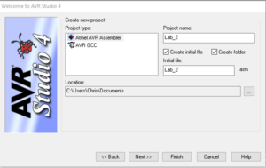
- Select AVR Simulator from the list of Debuggers and Atmega32U4 from the list of devices.
- Copy all of the code from the Lab1.asm file to the empty Lab_2.asm file.
- Copy the robot3DoT.inc file and upload.bat file from the Lab 1 folder to the Lab 2 folder.
- Assemble the code to make sure that it builds with zero errors and zero warnings.
How the AnalogWrite Subroutine Works
As mentioned in Prelab 2, the AnalogWrite subroutine is meant to be equivalent to the analogWrite() function used in the Arduino IDE. It is used to configure the speeds of each motor based on inputs provided by the user. The range of acceptable values used to represent the various speeds are from 0 to 255. While 255 corresponds to the fastest the motors can turn, 0 does not necessarily correspond to the motor moving at the lowest speed. It is more accurate to say that 0 would be equivalent to the motor being off and that there is a range of values where the motor is on but unable to turn. This is because those values represent the pulse width modulation duty cycle with 0 being 0% and 255 being 100%. It translates into a voltage being applied to the motors between 0 V and 5 V.
As this is a new subroutine, there are a few things to keep in mind. Unlike WriteToMotors, AnalogWrite requires two inputs and does not have any outputs. You will need to provide the two input values through registers 24 and 22 respectively. The values for each of these will have to be in hexadecimal. R24 is assigned to Motor A (left motor) and R22 is assigned to Motor B (right motor). If the values are not prepared properly before calling AnalogWrite, the subroutine will use whatever values were in those registers at the time and could result in unexpected results. That is why one of the rules for subroutines is to always load the arguments before calling the subroutine. More information about these rules that have not been covered so far are listed in Appendix A.
With this information, we can move onto the main focus of Lab 2.
Find the Maximum Speed
There is a high probability that your two motors are not equal. This is typically due to a difference in the internal friction of the gears and motors, which translates into a difference in the speed of rotation at a given voltage or duty cycle. This will cause your robot to veer towards the right or left. In order to address this issue, we will be start by finding the ideal maximum speed for the fastest motor such that the robot travels in a straight line (or at least as close as possible).
This portion of the lab involves a lot of trial and error. We will be placing the robot on the printed maze and verifying if it is moving in a straight line. If it reaches the room boundary without moving towards a side wall, then you have found the appropriate speed on each motor. If not, try changing the speed of one of the motors and check the result. You will be manually controlling the speed of each motor using the AnalogWrite subroutine. Add the following lines of code to the main loop.
...Previous Code...
     ldi r24, 0x05
     call WriteToMotors

     ldi r24, 0xFF     // value for speed of Motor A, left motor
     ldi r22, 0xFF     // value for speed of Motor B, right motor
     call AnalogWrite  // sets speed of both motors using inputs r24 and r22.

     rjmp loop
Begin with both motors running at full speed (PWM value of 255) and record in which direction the robot drifts towards. If it drifts to the right, then the left motor is faster than the right. Decrease the speed of the faster motor by lowering the duty cycle (PWM) of the faster motor. Repeat this process until the motors are in sync. Define the maximum speed for both motors as RightHIGH and LeftHIGH respectively with the following assembly directives. Make sure these directives are added before RST_VECT and after .INCLUDE < m32u4def.inc >.
.EQU RightHIGH = 0x____ (Fill in with the value that you determined. It should be between 0 and 255).
.EQU LeftHIGH = 0x____
With this, you will be able to use the terms RightHIGH and LeftHIGH instead of values that were determined in the exercise. For example, ldi r24, 0xFF would become ldi r24, LeftHIGH.
Find the Minimum Speed
Now that you have found the maximum speed, the next step is to find the minimum speed that will keep the motors synchronized and provide a safe margin above the stall speed for both. A motor will stall when there is insufficient power to the motor to overcome the internal friction of the gears and motor (i.e., nothing is moving). The motor is ON at this point and it is consuming power but there is no physical motion. This may damage the motor and should be avoided. By obtaining the minimum speed to get the motor moving, we can keep the motor ON and barely moving while the robot smoothly gets back on track. Make sure to find a speed that has the wheel moving at a reasonable pace. We do not need it to be barely moving but it should be distinguishable from the maximum speed. Feel free to go about 10 or 15 more than the lowest value that satisfies these conditions.
Using trial-and-error, determine the minimum speed for each motor. Specifically, slowly decrease the duty cycle (PWM value) until the minimum speed is reached with a margin of safety. If you pick a value where the motors are not turning, turn off the robot immediately to prevent damage. This should never happen as the AnalogWrite subroutine will default to a value of 0x50 if anything lower is inputted. If it seems like the value could go lower than 0x50 for your motors, please inform your lab instructor.
Next, run both motors at their minimum speed and note how the robot deviates from the line. Increase the speed of the slower motor. Repeat this process until the motors are in sync. We are not looking for just the minimum speed of each motor but the minimum speed for both to still move in a straight line. Define the minimum speed for both motors as RightLOW and LeftLOW. If you have the time and want your robot to move through the maze in a reasonable amount of time, the motors should be set to a value in between the maximum and minimum that is able to move in a straight line. This is optional as the minimum speed is enough to make it through the maze.
Once you have defined all of these values, Lab 2 is complete.
Lab 2 Deliverable(s)
|
All labs should represent your own work – DO NOT COPY. Submit your list file as defined below. Make sure that the code compiles without any errors. Do not forget to comment your code. Lab 2 Demonstration
|
Appendix A: Rules for Working with Subroutines
In the last lab I introduced three steps for writing a program for a load-store RISC based architecture.
- Load the data (lds),
- Do something (typically an arithmetic or logical instruction), and then…
- Store (sts) the result.
When working with subroutines an analogous set of steps applies.
- Load argument(s) into input registers (parameters) specified in the header of the subroutine. Following the gcc C++ calling convention, this would be register r24 if only one calling argument is specified (lds r24, myData).
- Call the Subroutine
- Do something with the return value(s) stored in the output register(s) specified in the header of the subroutine. Following the gcc C++ calling convention, this would be register r24 if a single byte value is returned. In most cases you will storing this return value(s) into SRAM data memory (sts myData, r24).
You call a subroutine using the rcall or call assembly instruction and return using the ret instruction. Here are a few rules to remember when writing your main program and subroutines.
- Your subroutine should always include a header block. As a minimum, the header must define the input arguments to the subroutine, the values returned, and what if any registers are modified by the subroutine.
- Always initialize variables and registers at the beginning of your program. Do not re-initialize variables or registers within a loop or a subroutine. For example, you only need to configure the port pins assigned to the switches once.
- Never jump into a subroutine. Use a call instruction to start executing code at the beginning of the subroutine.
- Never jump out of a subroutine. Your subroutine should contain a single return (ret) instruction as the last instruction.
- You do not need an ORG assembly directive. As long as the previous code segment ends correctly (rjmp loop, ret, reti) your subroutine can start at the next address.
- Subroutine names start with a capital letter.
- Your subroutine should contain only one return instruction (ret, reti) located at the end of the subroutine (last instruction). All blocks of code within the subroutine should exit the subroutine through this return (ret).
- Push (push r7) any registers modified by the subroutine at the beginning of the subroutine and pop (pop r7) in reverse order the registers at the end of the subroutine. This rule does not apply if you are using one of the registers or SREG flags to return a value to the calling program. Comments should clearly identify which registers are modified by the subroutine.
- You cannot save the Status Register SREG directly onto the stack. Instead, first push one of the 32 registers on the stack and then save SREG in this register. Reverse the sequence at the end of the subroutine.
push r15
 in r15, SREG
 :
 out SREG, r15
 pop r15
- Once again, never jump into or out of a subroutine from the main program or any other subroutine. However, subroutines may call other subroutines.
Assembly Robot Prelab 3 – Understanding the IR Sensors and Logic Operators
Table of Contents
Introduction
The focus of this prelab is to help you understand how the IR sensors function, what needs to be done with that information to obtain the desired output and review the logic operations that will be used in this class. All of this will be used in Lab 3 to implement the wall following logic needed for all subsequent labs.
What is a QRE113 Sensor?
As indicated in the figure above, the IR Shield has four QRE1113 sensors that output to the 3DoT board. The shield’s QRE1113 IR reflectance sensor is comprised of two parts – an IR emitting LED and an IR sensitive phototransistor. When you apply power to the VCC and GND pins, the IR LED inside the sensor will illuminate. A 100Ω resistor is on-board and placed in series with the LED to limit current. A 10kΩ resistor pulls the output pin high, but when the light from the LED is reflected back onto the phototransistor, the voltage at the output will begin to go decrease. The more IR light sensed by the phototransistor, the closer to zero it will go.
These sensors are widely used in line following robots because of how the output varies based on the reflective properties of the material below it. In general, white surfaces reflect much more infrared light than black, so, when directed towards a white surface, the voltage output will be lower than that on a black surface. This is due to the black surfaces absorbing the IR light, which results in the 3DoT board interpreting it as an output of 1 (digital logic HIGH) . When on a white surface, the output will be seen as a 0 (digital logic LOW).
With this in mind, you may see what needs to be done in order to implement the wall following logic that was discussed in the Lab 1 design challenge. To prepare you for Lab 3, please answer the following questions.
Question 1 – As only two IR sensors will be needed for a simplistic wall following algorithm, which motor driver pins should they be connected to? Consider which pins will require the least additional code to implement. Mention any extra steps needed for your choice to work. We want the robot to correct its movement if it runs into a wall and to keep going forward.
Question 2 – What assembly instruction can be used to save a specific bit value from a register? Where is that information saved to?
Why are there so many names for one wire?
One thing you may find confusing, is all the names and numbers associated with each input. Looking at the right sensor we see the somewhat confusing A0 plus PF7(ADC7), IR_R-O. The A0 mnemonic is the name assigned by the Arduino community and the one we would use if we were programming within that Arduino IDE. The second PF7(ADC7) is the name given to the pin by Atmel. It has two mnemonics PF7 and ADC7 because this pin is shared by two peripheral subsystems – GPIO Port F and the Analog to Digital Converter (ADC). We are reading the sensor as a digital input and so the name we want is PF7. Mnemonic IR_R-O is defined in robot3DoT and is equated to PF7. Believe it or not this was done to make the code more readable as it is clear what the pin is being used for.
Logic Operation Review
As we begin to solve more complex problems with our programs, you will find that it is not possible to accomplish the desired output by simply connecting the input directly to the outputs. There will be cases where the inputs need to be manipulated in some way before being sent to the outputs. There may be some decoding or applying boolean logic in our programs. To prepare for that, we will review the basic logic operations that can be performed with the assembly instructions. Keep in mind that all of these operations are bit-wise even when applied to entire registers. Please fill in the tables with the correct outputs.
| Logic Operation | Bit #1 | Bit #2 | Output |
| AND | 0 | 0 | |
| 0 | 1 | ||
| 1 | 0 | ||
| 1 | 1 | ||
| OR | 0 | 0 | |
| 0 | 1 | ||
| 1 | 0 | ||
| 1 | 1 | ||
| EOR (Exclusive OR) | 0 | 0 | |
| 0 | 1 | ||
| 1 | 0 | ||
| 1 | 1 | ||
| COM | 0 | X | |
| 1 | X |
| Logic Operation | Register #1 | Register #2 | Output |
| AND | 01101010 | 11000110 | |
| AND | 0xA8 | 0x75 | |
| OR | 10011101 | 10100110 | |
| EOR | 0x5D | 0xF4 |
Prelab 3 Deliverable(s)
Page 1 – Title Page with Name, lab title, and photo
Page 2 – Answers to questions and completed tables
Assembly Robot Lab 3 – Creating the ReadSensor Subroutine and Implementing Wall Following
Table of Contents
Introduction
This lab is designed to help you understand how to create your own subroutines and the reasoning behind the rules/guidelines for subroutines. The bulk of future labs will revolve around designing subroutines for specific tasks and utilizing them in the main loop of the program. The focus of this lab is to make the ReadSensors subroutine which will take in the inputs from the two inner IR sensors and place them in the appropriate locations to control the motors for the wall following algorithm. By the end of this, you will have completed the first major milestone towards getting the robot to navigate through the maze.
What Is New
The following instructions and assembly directives are used in Labs 1. If you have any questions on any instructions or assembly directives a nice source of information, in addition to your textbook, are AVR Instruction Set Manual and the Atmel AVR Assembler User Guide.
AVR Assembly Instructions
Bit & Bit Test
bst R17,5      // Copy the bit value from register 17 bit position 5 to the T bit of SREG.
bld R19,2      // Loads the bit value from the T bit of SREG to register 19 bit position 2.
Arithmetic and Logic
com R19 // Takes the one's complement of the value in register 19.
Control Transfer
brtc Cond_1   // Branch if the T bit is clear to Cond_1 label.
brts Cond_2   // Branch if the T bit is set to Cond_2 label.
rcall Test    // Relative call to the subroutine Test. Similar to call instruction except for range and memory efficiency.
ret           // Return from a subroutine. Must be the last instruction of that subroutine.
Key Points on Creating A Subroutine
As mentioned in previous labs, there are several things to keep in mind when dealing with subroutines. They can be used to keep the program organized, are designed with repeated uses in mind, and have a general structure to follow. We will review these details as it pertains to the ReadSensors subroutine for this lab.
WHY SUBROUTINES?
- Divide and Conquer – It allows you to focus on one small “chunk” of the problem at a time.
- Code Organization – Gives the code organization and structure. A small step into the world of object-oriented programming.
- Modular and Hierarchical Design – Moves information about the program at the appropriate level of detail. This is similar to the top level flowchart from Prelab 1 (TakeAStep, EnterRoom, WhichWay).
- Code Readability – Allows others to read and understand the program in digestible “bites” instead of all at once. Higher level subroutines with many lower level subroutine calls take on the appearance of a high level language. Rather than having to go through several hundreds of lines of code that could have repeating sections, others can see the abbreviated version with subroutine calls and look for additional details if needed.
- Encapsulation – Insulates the rest of the program from changes made within a procedure. This limits the effect of minor changes within the subroutines on the overall program as long as it does not affect the main algorithm.
- Team Development – Helps multiple programmers to work on the program in parallel; a first step to configuration control. Allows a programmer to continue writing his code, independent of other team members by introducing “stub” subroutines. A stub subroutine may be as simple as the subroutine label followed by a return instruction. As long as they follow the standard convention, they do not need to worry about potential issues with how the data is handled.
SUBROUTINE STRUCTURE
You should use the following template when creating your subroutines.
; —- My Subroutine ——-
; Called from Somewhere
; Input: Value of registers, SRAM variables, or I/O registers placed into specific registers
; Outputs: None or specific registers depending on the number of outputs. Could be register pairs for a C function
; No others registers or flags are modified by this subroutine than those indicated.
; Temporary registers will have their values original restored.
; ————————–
MySubroutine:

push r15 // Saves original value to the stack
in r15,SREG // Saves current value of flags
push r16 // Frees up register 16 as a temporary register

your assembly code

endMySubroutine:

clr r25 // zero-extended to 16-bits for C++ call (optional)
pop r16 // Restore original value of register placed on the stack
out SREG,r15 // Restores original value of flags
pop r15 // Pops original value of register placed on the stack
ret
The first thing you should notice about this template is the header block or comment section. The purpose of this is to provide the relevant information about your subroutine without having to look through the assembly instructions and figure it out. It helps tremendously when you have not worked with the code after a long period of time or when you need to answer questions during a lab demonstration. You must always have this header block.
The second thing to note are the labels used within the subroutine. The very first label (MySubroutine) indicates where the section of code starts and is the name used whenever the subroutine needs to be executed. Additional labels can be used within the subroutine such as endMySubroutine to help keep things organized. One important convention that we are going to be using with subroutines is that the name of the subroutine must start with a capital letter and is in camel case. Camel case is where the beginning of each word in the string is capitalized and all other letters are lower case, similar to humps on a camel. This is why MySubroutine was written this way. endMySubroutine is written differently to distinguish it as a normal label and not the name of the subroutine.
The third thing to consider is how data is sent to and from the subroutine if it is needed for any calculations or modification. This is seen with the push and pop instructions at the beginning and end of the subroutine. Some of the ways to do this are listed below.
- In Register(s) or Register Pair(s) agreed upon between the calling program and Procedure or Function.
- By setting or clearing one of the bits in SREG (I, T, H, S, V, N, Z, C).
- In an SRAM variable, this method is not recommended.
- As part of a Stack Frame, this method is beyond the scope of a course on microcontrollers but is highly recommended.
For this class, we will be using register(s) or register pair(s) as mentioned in Prelab 2. Specifically, using R24, R22, and/or R20 for varying numbers of inputs / outputs. Due to this designation, you must always initialize those input values before calling the subroutine. If the input is an SRAM variable, a constant, or a value from another register, make sure to use the appropriate instruction to place it into the register (R24 and so on). Do not re-initialize variables or registers within a loop or a subroutine. For example, you only need to configure the port pins assigned to the switches once. The reasoning behind this is to make it clear what is being sent to the subroutine. If the variables or registers were changed within the subroutine, the reader would not be aware of it without taking the time to look through the subroutine.
If additional temporary registers are needed for the calculations within the subroutine, choose which ones will be used and save the original value to be restored when the subroutine is finished. Push (push r7) any registers to be modified by the subroutine at the beginning of the subroutine and pop (pop r7) in reverse order the registers at the end of the subroutine. This rule does not apply if you are using one of the registers or SREG flags to return a value to the calling program. This means that you should never push or pop R24, R22, or R20. Comments should clearly identify which registers are modified by the subroutine.
You may notice from the template that another temporary register is used to store the value of the Status Register at the beginning of the subroutine. This is to preserve the flag values in case they are used for anything outside of the subroutine. The other instructions in the subroutine could modify them and this will ensure that no problems occur. You cannot save the Status Register SREG directly onto the stack, which is why we push one of the 32 registers on the stack and then save SREG in this register. Remember to reverse the sequence at the end of the subroutine.
The final thing to remember about subroutines deals with the way the program flows. This includes how you get into a subroutine, how you can move within it, and how to leave it.
- Never jump or branch into a subroutine. Use a call instruction to start executing code at the beginning of the subroutine. The idea here is that you should not go to a specific label within the subroutine and start executing from there. If you need that specific part to be used many times, it may be a good idea to turn it into a separate subroutine.
- Never jump out of a subroutine. Your subroutine should contain a single return (ret) instruction as the last instruction. This is because the call instruction remembers where to go back to once the subroutine is complete. If the return instruction is not used, that value is still saved and taking up unnecessary space.
- Your subroutine should contain only one return instruction (ret, reti) located at the end of the subroutine (last instruction). All blocks of code within the subroutine should exit the subroutine through this return (ret).
Defining the ReadSensors Subroutine
Creating Lab 3
As we are continuing on from Lab 2, make sure to do the following when creating Lab 3.
To start, create a new project in AVR Studio 4.
- Give the lab an appropriate name and make sure the options to create the initial file and folder are selected.
- Select AVR Simulator from the list of Debuggers and Atmega32U4 from the list of devices.
- Copy all of the code from your Lab2.asm file to the empty Lab3.asm file.
- Copy the robot3DoT.inc file and upload.bat file from the Lab 2 folder to the Lab 3 folder.
- Assemble the code to make sure that it builds with zero errors and zero warnings.
The ReadSensors Subroutine
With those details out of the way, we can now focus on creating the ReadSensors subroutine. Before we begin writing the code, you will need to understand what the subroutine is trying to accomplish.
In Labs 1 and 2, we have been learning how to control the motors accurately and working with the sensors. If you completed the Lab 1 design challenge, you also have a very simple version of wall following. The end goal of Lab 3 is to have an improved wall following algorithm that will minimize possible issues with moving through the physical maze in future labs. You may have noticed from lab 1 that the robot sometimes ignores the walls despite the wall following algorithm that was put into place. This is due to the thickness of the lines and the momentum of the robot as it is moving. We may need to use a different tactic if this solution does not resolve this issue but that will be addressed once you have the robot kits to experiment with. In this lab, the wall following algorithm will force the appropriate motor to run at the minimum speed that you discovered in Lab 2 rather than try to stop it completely. This will also address the concern of the robot stopping completely when it reaches the boundaries of a room as the black line going across the room horizontally should cause both motors to stop. With this change, it will slow down as it crosses the boundary and continue into the next room.
For this wall following algorithm, the two inner sensors will need to be linked to the motors in some way. There are many possible solutions for this but we will be focusing on using the sensor data to determine the speed the motor should be moving at. Most students would consider linking the sensors to the motor driver pins as the most logical approach and it can be done. The issue with that implementation is that by linking the sensors to the motor driver pins, you are changing the direction that the motors are moving. When the motor was originally going forward, you may now accidentally cause it to go in reverse or to be free wheeling if it is in the coast state. While the robot may be small, inertia is still something that can cause problems when the motors suddenly change directions. This is why it is more effective to control the motor speed instead.
If you remember what was mentioned in Prelab 3, the IR sensors return a value of 0 for any white or reflective surfaces. It returns a value of 1 for any black or absorptive surfaces. As the robot will be on white for the majority of the time, it should be moving at the high speed when that is detected. This is where we can make a decision on how the data is used to represent different situations or results. If the raw values are used, then a 0 from the sensors should correspond to the motor running at the high speed and a 1 should correspond to a low speed. However, since we have the freedom of deciding how the information is interpreted and executed, it can be reassigned in a way that is more intuitive for us. Since we usually associate a 1 with a digital high, we can keep things consistent where a 1 can be used to represent the high speed for a given motor. That means we want to take the opposite of what the sensor is detecting and that is accomplished with the complement instruction. You will also want to consider which motor each sensor is controlling, which we will discuss later.
In addition to this, the direction of the motors need to stay the same (going forward). This means you will still need to prepare the configuration value to be sent to WriteToMotors. This is where we can determine what the inputs and outputs for the ReadSensors subroutine should be. You could consider the IR sensors to be an input as well but they can be brought into a temporary register in the subroutine rather than be an input provided at the beginning. That leads us to the template shown below. Make sure to fill in the details for the comment section on this subroutine.
; --- ReadSensors ---
; Called from the main loop
; Inputs:
; Outputs:
; Purpose:
ReadSensors:
     push r15
     in r15, SREG


    ... space for more code ...

endReadSensors:
     out SREG, r15
     pop r15
     ret
Place this code after the rjmp loop instruction from the main loop. All student created subroutines will be going here in the future. The reason this is possible is because we have designed each subroutine to stay within its own section indicated by the subroutine name and the ret instruction. As they are isolated, they will not be executed except for when they are called from the main loop.
In order to complete the subroutine, you will need to make use of the com, bst, and bld instructions. First, we will need to prepare a temporary register to hold the value from the IR sensors. Choose any of the remaining registers besides R22 and R15 for this. In this example, R18 was used. Once that is done, you can add the assembly instruction to bring in the sensor values from PINF. It should look something like the following. Don’t forget to add the corresponding pop in the correct order.
ReadSensors:
     push r15
     in r15, SREG
     push r18

     ... space for more code ...

endReadSensors:
     pop r18
     out SREG, r15
     pop r15
     ret
After that, we need to discuss how the bst and bld instructions work. They stand for bit store and bit load respectively. Both instructions utilizes the T flag in the status register as a storage location for a bit value. To save something to it, you wil need to specify the register and bit location. For example, bst r18, 3 will take the fourth bit in register 18 and copy it to the T flag. On the other hand, the bit load instruction needs the destination register and bit location. For example, bld r22, 2 will take the current value of the T bit and overwrite the value of the third bit in register 22. The two instructions are typically paired together to make sure that the value is not lost in case some other instruction modifies the T flag. Add in the rest of the code needed to complete the subroutine. In order to simplify things, we will use bit position 1 of R22 to represent the speed of the left motor and bit position 0 to represent the speed of the right motor. Make sure to take the information from the appropriate sensor and place it in the right spot. The final output from this subroutine will have the motor speeds in bits 1 and 0 to be analyzed in the main loop.
Now, we need to add the call to the subroutine in the main loop. Your code should look like this.
loop:
    ldi r24, 0x05
    call WriteToMotors
    call ReadSensors
    ldi r24, LeftHIGH
    ldi r22, RightHIGH
    call AnalogWrite
    rjmp loop
Modified Wall Following Algorithm
With the ReadSensors subroutine completed, we have implemented the simple wall following algorithm. However, this only address if the motor is on or off and not the speed that the motors are running at. This will require us to modify the code in order to set the speed for the appropriate condition. It should be set to the maximum speed if the IR sensor is not on the line and the minimum speed if it is. That leads us to the usage of branching instructions and how they are used for implementing conditional statements.
Additionally, it would be wise to copy the output from the ReadSensors subroutine to another register as register 24 is used as a common register for many of our subroutines. The data will end up being overwritten when we set the speed of the robot with AnalogWrite.
Conditional Speed Setting
From the ReadSensors subroutine, you know that the motors should be going at maximum speed if a 1 is being placed into R24 and it should be at minimum speed if a 0 is placed. A branching instruction can be used to detect and handle both cases. Specifically, we will be using the brtc and brts instructions as we are dealing with one bit per motor. The way these instructions operate is that they will only trigger if the condition is true. For example, btrc will only trigger if the T flag is clear or equal to 0. When it triggers, it will go to the label that was defined with the instruction. It proceeds to the next instruction instead if the condition was false. Examples 1 and 2 show which lines of code are executed depending on the condition.
Example 1 (T Flag = 0)                 Example 2 (T Flag = 1)
brtc Test                              brtc Test
mov r16, r20                           mov r16, r20
mov r19, r22                           mov r19, r22
rjmp loop                              rjmp loop

Test:                                  Test:
    ldi r20, 0x0F                      ldi r20, 0x0F
    ldi r22, 0x3C                      ldi r22, 0x3C
    rjmp loop                          rjmp loop
These are just examples. Do not put this in your code.
Using this, write the code to set the speed of the motors appropriately. For example, the code could look something like this. You have the freedom to use different names for the labels but the ones used have been chosen to help indicate what is happening in the code.
loop:
    ldi r24, 0x05
    call WriteToMotors
    call ReadSensors
    ... Code to check proper bits ...
    brts rightmax // Check if sensor is not on the line. Go to label leftmax if true.
    leftoff: // Label to indicate that this handles if the sensor was on the line.
         ldi r24, LeftLOW
         rjmp checkright   // go to check the right motor

    leftmax:  // Label to indicate that this handles if the sensor is not on the line.
         ldi r24, leftHIGH
         rjmp checkright

   ... Rest of the code ...
   rjmp loop
Complete the rest of the code and verify if the robot is changing speeds correctly.
Lab 3 Deliverable(s)
|
All labs should represent your own work – DO NOT COPY. Submit your list file as defined below. Make sure that the code compiles without any errors. Do not forget to comment your code. Lab 3 Demonstration
|
Assembly Robot Prelab 4 – Working with Timers and Delays
Table of Contents
Introduction
The focus of this prelab is to help you understand how the timers operate and prepare you to write the code needed to configure them for a specific delay.
Basics about Timers
As discussed in lecture, there are several ways the microcontroller can keep track of time and be programmed to execute specific actions after a delay. It can be done with a loop that has been designed to use up that amount of time or handled by a separate system. That is where the timers come in. They are configurable counters that can be set up for a wide range of applications such as:
- Turn on or turn off an external device at a programmed time.
- Generate a precision output signal (period, duty cycle, frequency). For example, generate a complex digital waveform with varying pulse width to control the speed of a DC motor
- Measure the characteristics (period, duty cycle, frequency) of an incoming digital signal
- Count external events
All of these functions are done manually or automatically depending on how the timer is configured. The ATmega32u4 has four timers in total. Timer 0 is an 8 bit timer, Timer 1 and 3 are 16 bit timers, and Timer 4 is a 10 bit high speed timer.
Important Terminology
Before we get into the calculations and configuration, there are some key terms to understand.
Frequency
The number of times a particular event repeats within a 1-s period. The unit of frequency is Hertz, or cycles per second. For example, a sinusoidal signal with a 60-Hz frequency means that a full cycle of a sinusoidal signal repeats itself 60 times each second, or every 16.67 ms. For the digital waveform shown below, the frequency is 2 Hz.
Period
The flip side of frequency is the period. If an event occurs with a rate of 2 Hz, the period of that event is 500 ms. To find a period, given a frequency, or vice versa, we simply need to remember their inverse relationship, where F and T represent a frequency and the corresponding period, respectively.
Duty Cycle
In many applications, periodic pulses are used as control signals. A good example is the use of a periodic pulse to control a servo motor. To control the direction and sometimes the speed of a motor, a periodic pulse signal with a changing duty cycle over time is used.
Duty cycle is defined as the percentage of one period a signal is ON. The periodic pulse signal shown in the Figure 1 is ON for 50% of the signal period and off for the rest of the period. Therefore, we call the signal in a periodic pulse signal with a 50% duty cycle. This special case is also called a square wave.

Figure 1: Digital Waveform
One key thing to keep in mind here is that the amount of time that the signal is HIGH can vary from the amount of time that it is LOW depending on the duty cycle. For figure 1, they are the same. This allows the programmer to use the same delay to generate this signal on an output pin. Due to this, the delay to configure the timer for does not always match with the period of the desired signal.
Timer Register Descriptions
With the terminology covered, we can now focus on the timer registers that you will be working with in the lab. As mentioned earlier, there are many ways that the timers can be used as shown in Figure 2. It is important to note that these registers are not part of the general purpose registers that are in the AVR CPU. They are located within the Extended I/O registers which are a part of the SRAM address space, not the I/O address space. We are only concerned with the normal mode which will increment by 1 until it reaches the maximum value 0xFFFF and then restarts at 0x0000 when it overflows. You may notice that there are terms for TOP, BOTTOM, and MAX. These can be changed depending on the operating mode but you should consider MAX to be 0xFFFF and BOTTOM to be 0x0000 for our course.
As we are only working in normal mode, you will not need to modify any of the configuration registers besides TCCR1B which stands for Timer/Counter 1 Control Register B. This is because the default setting for the other registers is to start in normal mode.
The main bits that we are concerned about in TCCR1B are the clock select or CS bits. These bits allow us to define how quickly the timer will increment and ultimately how long it takes to overflow. The options for this are all based on the system clock signal coming from the microcontroller or an external clock source as indicated in Figure 4. You will need to select the appropriate combination for the bits in order to configure the timer for your desired delay. For example, if the pre-scale value of 256 is chosen with a system clock frequency of 16 MHz, the clock frequency for the timer will effectively be 62.5 KHz and result in a maximum delay of 1.0486 seconds.
The last of the registers that you will need to become familiar with are the timer counter registers (TCNT1H and TCNT1L) and the timer interrupt flag register (TIFR1). They are relatively self explanatory, with the timer counter registers holding the current value before the next increment and the timer interrupt flag register holds the status of the flags. We are mainly concerned with the TOV1 bit which indicates if the timer has overflowed (becomes 1) or not. One important thing to keep in mind is that the timer does not automatically tell the microcontroller that the overflow has occurred unless the corresponding interrupt was configured. If that has not been set, the microcontroller will only know that the timer is finished when it is programmed to check the value of the TOV1 bit.
Calculating the values for a specific delay
Maximum Delay
So can TCNT1 generate the 250 ms delay required to generate our 2 Hz square wave? To answer that question, we will need to determine the maximum delay possible. Assuming a system clock frequency of 16.000 MHz and a pre-scale divisor of 64, the largest time delay possible is achieved by setting both TCNT1H and TCNT1L to zero, which results in the overflow flag TOV1 flag being set after 216 = 65,536 tics of the Timer/Counter1 clock.
fT1 = fTclk_I/O/64, given fTclk_I/O = fclk then fT1 = 16.000 MHz / 64 = 250 KHz
and therefore T1max = 65,536 tics / 250 KHz = 262.14 msec
Clearly, Timer 1 can generate a delay of 250 msec. Our next step is to calculate the TCNT1 load value needed to generate a 250 ms delay.
Step to Calculate Timer Load Value (Normal Mode)
To generate a 250 msec delay assuming a clock frequency of 16 MHz and a prescale divisor of 64.
Variables
tclk_T1 – Period of clock input to Timer/Counter1
fclk – AVR system clock frequency
Solution
- Divide desired time delay by tclk_T1 where tclk_T1 = 64/fclk = 64 / 16.000 MHz = 4 µsec
250msec / 4 µs = 62,500 - Subtract 65,536 – step 1
65,536 – 62,500 = 3,036 - Convert step 2 to hex.
3,036 = 0x0BDC
Questions
Question 1 – Calculate the maximum delay that can be generated with Timer 4 when the system clock frequency is 16 MHz and the selected pre-scale value is 256. Keep in mind that the number of bits used for Timer 4 and and time for each count/increment is needed to solve this problem.
Question 2 – Calculate the value to be loaded to the Timer 0 Counter Register in order to have a delay of 218 microseconds if Timer 0 is used with a system clock frequency of 20 MHz and a pre-scale value of 64.
Question 3 – Calculate the value to be loaded to the Timer 3 Counter Register in order to have a delay of 2.43 seconds if Timer 3 is used with a system clock frequency of 16 MHz. The pre-scale value is not given and must be determined. Make sure to select the lowest value possible that will work.
Question 4 – Write the lines of code needed to implement the configuration listed in Question 3. Keep in mind that the names of the registers for the timers is exactly the same except for the timer number. IE TCCR1B vs TCCR3B.
Prelab 4 Deliverable(s)
Page 1 – Title Page with Name, lab title, and photo
Page 2 – Answers to questions. Make sure to show all of the work involved with getting to the answer.
Assembly Robot Lab 4 – Handling the Intersections with Delays and Interrupts
Table of Contents
Introduction
This lab is designed to help you understand how timers, interrupts, and finite state machines can be used to implement a method for how the robot moves through the maze. In the previous labs, we have only been concerned with getting the robot to move in a straight line and correct itself if it veers off course. An issue that we did not address is when the robot reached the end of one room and moved into the next one. It ignored the fact that the robot might need to turn or change course at that location. We will now be addressing that so that the robot will briefly stop at the center of a room. You will be using delays, interrupts, and finite state machines in order to perform wall following when needed and to be able to do a different action when the robot has reached the center of a room. By the end of this lab, we should have the basic structure that we will be building upon in the remaining labs.
What Is New
The following instructions and assembly directives are used in Lab 4. If you have any questions on any instructions or assembly directives a nice source of information, in addition to your textbook, are AVR Instruction Set Manual and the Atmel AVR Assembler User Guide.
AVR Assembly Instructions
Data Transfer
lds r24, variable      // Load value from variable(or location in SRAM) to register 24
sts variable, r16      // Store value from register 16 to variable (or location in SRAM)
push r17               // Save the value from register 17 to the stack temporarily
pop r19                // Copy the last value from the stack to register 19.
Arithmetic and Logic
cbr r24, 0b01101101     // Clear the bits in register 24 designated with a value of 1. Locations with a value of 0 are left the same.
tst r16                 // Check to see if the value in register 16 is equal to zero or negative (does the AND operation with itself).
Control Transfer
cpi r24, 0x3C         // Compares the value in register 24 to the constant 0x3C
reti                  // Return from Interrupt Service Routine (will re-enable global interrupts)
sei                   // Set the I bit in SREG (enable global interrupts)
AVR Studio Assembly
Directives
.DSEG                       // Indicates the start of the Data Segment (SRAM)

example: .BYTE X      // Defines an SRAM variable called example that is in terms of bytes and takes up X bytes. (IE X=3 means it takes up 3 bytes)
Breaking the Objective into Parts
At the end of Lab 3, you should have gotten your robot to continuously move in a straight line while staying within the walls and be able to cross over intersections at a slower speed instead of stopping. We will now be focusing on getting to the center of a room and performing an action after that. As it is, the program from Lab 3 is suited for the parts of your path that are straight lines but is not capable of changing directions. We want to be able to separate that section of code from the main loop and execute it when the conditions are right. The end goal of Lab 4 is to have the robot detect that it is at the end of a room, cross into the new room and move to the center of the room, and then spin in place. The spinning in place is a temporary output to show that the robot has switched from the wall following algorithm to making a decision after it has entered a room in the maze. From this high level concept, we will go over how it can be broken down into the code that needs to be added.
In order to implement this, the first key change is that there are two situations that the robot should be running through depending on the position of the robot. The first one is that the robot should be executing the wall following algorithm if the edge of a room has not been encountered. The second one is to perform the spinning action after it has reached the center of the next room. While there are many ways that this can be implemented, we will be using a finite state machine to handle the two situations as a part of the main loop. It provides a structure that separates the two sections of code and allows for expansion if more states are needed.
For the finite state machine to work, there are four things that need to be discussed further.
- The structure of the main loop needs to be changed in order to execute the appropriate state at any given point in time.
- There needs to be something to keep track of which state should be executed. This can be done with a variable that represents the next state to go to.
- The next state variable needs to update when the edge of the room is detected.
- The updating of the variables should occur automatically without having the program wait for something to happen.
The first two issues will be handled by the finite state machine and the next state variable that we will be creating. The third issue will be dealt with during the wall following state as that is when the transition should be occurring. The last issue is where the timer and the overflow interrupt will be used. As many of these parts are interconnected with each other, they will be covered in the order that is the easiest to follow.
One final issue that can make this lab seem too complicated to follow is where the robot starts to execute its spin. While it will not be a problem right now, it can greatly affect your rate of success with going through the entire maze. This is because as the robot is moving, there are several factors such as the battery power remaining, the friction on the wheels, and other things that affect how fast the motors move. This leads to the robot missing the walls or being in a position where it cannot recover with the wall following algorithm. Additionally, the position of the robot when it begins the turn plays a big role in this problem. In order to make sure this is not an issue, we will make sure that the robot is in the center of the room before it begins to spin.
The solution that we will be using here is to utilize a timer to trigger the transition between states. By turning a timer on when the edge of a room is detected, we can avoid adding several conditional checks or looping until the robot has crossed the line and is in the center of the room. It also allows the robot to continue executing the wall following, which does not change any of the code as we will wait until the timer overflows. The timer overflow interrupt will then update the next state variable so that the spin action will be executed. This requires us to have determined the right amount of time before the overflow occurs as it can vary based on the motor speeds. However, that is easier to take care of than the alternatives.
Finite State Machine
The following figure shows the general process that the finite state machine will follow.
When the robot is turned on, it will automatically start with State 0. This is to make sure the robot can move forward and follow the line to the next room in the maze. As long as the intersection is not detected, it will keep running State 0. The moment an intersection is detected, it will trigger the change to State 1 but it will not be going there right away. We are using Timer 1 to delay the transition for a certain amount of time so that the robot is in the center of the room. It will still be executing State 0 until Timer 1 has overflowed. All of this can be represented with the following flow chart.
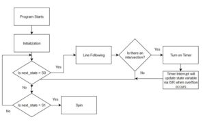 Once the transition has occurred, it will go to State 1 and then spin in place. In order to implement the finite state machine, the structure of our main program will be changed. The code that was in the main loop will need to be removed. As a starting point, you should have just the label and the rjmp loop instruction.
loop:

    // all other code has been removed

    rjmp loop
From here, the code can be broken into three parts. One section is used to determine the appropriate state to execute. Another section will produce the output needed for State 0 and the last section will handle the output needed for State 1. In later labs, modifications will be made to the sections as needed but the general structure will stay the same. This can be represented by the following diagram.
loop:
    // Code to determine which state to execute
    // Will branch or jump to appropriate labels


    // Code for State 0 output
    // Will branch or jump to endloop label when done

    // Code for State 1 output
    // Will branch or jump to endloop label when done

endloop:
    rjmp loop
For the first section, we will need to create a variable to keep track of the next state to execute and to check what value it is. Variables are different from registers in that the data is saved in SRAM and it cannot be accessed by the CPU directly. While this may seem like a downside, it does not take up one of the 32 registers and will persist as long as the program is running. It will help with the problem of running out of registers to hold data in and can be retrieved at any time. To define this SRAM variable, you will need to use the following format.
table: .BYTE 4
The first column is the label assigned to the SRAM address being reserved for the variable. You can use any name as long as it is valid. In this case, we want to call it next_state. The second column defines the data type. It can be in terms of bytes (8 bit values) or words (16 bit values). We will typically be dealing with bytes but be aware of the alternatives. The third column indicates the number of SRAM address to reserve. This is more or less the size of the variable. The example variable will reserve 4 bytes of space for the variable called table. Use this knowledge to define the next_state variable which needs only one byte of space. One final detail about defining SRAM variables is that it must be placed in a different section of our program as SRAM is part of the data segment while FLASH is part of the code segment. What this means is that you will need to insert the following lines above .CSEG
.INCLUDE

.DSEG
next_state: .BYTE 1

.CSEG
.ORG 0x0000
RST_VECT:
One common misconception people have about defining SRAM variables is that everything is ready to go once it has been defined. However, the starting value of the variable has not been defined. It will default to whatever value is currently at that SRAM address, which could potentially be any value. This means every SRAM variable will also need to be initialized in order to prevent any errors with calculations or checking which state to execute. The initialization is done by saving the desired value from a register to the SRAM variable. For the finite state machine, we want to define a value to represent the states. We will be defining the binary value of 00 as state 0 and 01 as state 1 as shown below with equate statements. From there, you can save the appropriate value.
// Equate statements
.EQU S0=0b00
.EQU S1=0b01

// Variable initialization
ldi r16, S0
sts next_state, r16
Now we can handle the code to determine what state to execute. As shown in the diagram at the beginning of the section, the main loop will begin by checking if next_state is equal to S0 or S1. As it is stored in an SRAM variable, you will need to load it into a register in order to perform a comparison as shown below.
loop:
    lds r17, next_state
    cpi r17, S0
    breq state0
    cpi r17, S1
    breq state1
    rjmp endloop
This will check what the value of next_state is for that iteration of the loop and branch to the appropriate state. If it does not match any of the valid states, it will not execute the code and go to the end of the loop. With that out of the way, we can focus on defining the code for State 0.
State 0 Output Code
The main output for State 0 is the line following code. This has already been completed from previous labs and will just be moved from the beginning of the main loop into this area. The only addition that needs to be made is to detect the intersection and to turn on Timer 1 in order to change the states. This will involve a slight change to the structure from Lab 3 that controlled the motor speeds.
To start, you will need to copy over the lines of code from Lab 3 that configure the motors to move forward, to get the values from the IR sensors, and to output it to the motors. The code should look something like this:
.INCLUDE m32u4def.inc

// These are arbitrary values. Make sure that you use your values from Lab 2
.EQU RightHIGH = 0xFF
.EQU LeftHIGH = 0xFF
.EQU RightLOW = 0xAF
.EQU LeftLOW = 0xAF

.EQU S0 = 0b00
.EQU S1 = 0b01

.DSEG
next_state: .BYTE 1

.CSEG
.ORG 0x0000
RST_VECT:
    rjmp reset
.ORG 0x0100
.INCLUDE "robot3DoT.inc"
reset:
    ldi R16, HIGH(RAMEND)
    out SPH, R16
    ldi R16, LOW(RAMEND)
    out SPL, R16
    call Init3DoT

    ldi R16, S0
    sts next_state, R16
loop:
    lds R17, next_state
    cpi R17, S0
    breq state_0
    cpi R17, S1
    breq state_1
    rjmp endloop

state_0:
    ldi R24, 0x05
    call WriteToMotors
    call ReadSensors
Next, we need to address the code to detect the end of a room. The code from Lab 3 checks one motor at a time and does not handle both at once. It also only changes the speed of each motor separately and could be improved on. As covered in lecture, we can make use of comparisons to evaluate what situation is being detected by the IR sensors. There will need to be some processing involved to make sure that we are only looking at the desired bits and nothing else. Since the values from the IR sensors are placed into R22 to implement wall following, we can use those bits to determine if the robot is hitting a line or an intersection. Specifically, that would be bit 1 and bit 0 which are the left and right motors respectively. As the remaining 6 bits could be any combination of values, we want to remove them from the equation so that it makes it easier to handle the comparisons. This can be done with the cbr instruction, which clears the indicated bits in a register. With that taken care of, we can use the cpi instruction in order to determine which of the four possible situations the sensors could be seeing. Those situations are listed below along with the value we should be expecting to see in register 22.
| Situation | Motor Speeds | Value in R24 |
| Robot staying within the walls (both on white) | Right – Max speed
Left – Max speed |
0b00000011 |
| Robot veering to the right (Left on white, Right on black) | Right – Min speed
Left – Max speed |
0b00000010 |
| Robot veering to the left (Left on black, Right on white) | Right – Max speed
Left – Min speed |
0b00000001 |
| Robot reaching the end of a room (both on black) | Right – Min speed
Left – Min speed |
0b00000000 |
We will now replace the branching structure that was used in Lab 3. The code will look like this.
state_0:
    ldi R24, 0x05
    call WriteToMotors
    call ReadSensors
    cbr R22, 0b11111100
    cpi R22, 0b00000011
    breq inside
    cpi R22, 0b00000010
    breq rightOnLine
    cpi R22, 0b00000001
    breq leftOnLine
next_Room:
Feel free to use different names for the labels. The ones chosen here are selected to be the most descriptive of what is happening. For the code that goes into each of the new sections, we will go over just two of the four. You will be expected to complete the rest.
The code for the next_Room section needs to turn Timer 1 on and is done with the following. Keep in mind that we have not determined the appropriate prescale value to use for the timer, so this is a preliminary number to use. Make sure to come back and update this value as needed.
next_Room:
    // Set motors to appropriate speed
    ldi R24, LeftLOW
    ldi R22, RightLOW
    rcall AnalogWrite
    // Load value to turn timer 1 on
    ldi R16, 0x01
    sts TCCR1B, R16
    rjmp endloop
The code for the other three sections only needs to change the motor speeds. It will look like the following. Make sure to handle each situation appropriately. Each of these labels can be placed after the previous rjmp endloop.
inside:
    ldi R24, LeftHIGH
    ldi R22, RightHIGH
    rcall AnalogWrite
    rjmp endloop
In the end, the code should look something like this.
State_0:
// Code for line following
    ldi R24, 0x05
    call WriteToMotors
    call ReadSensors
// Processing information from IR sensors
    cbr R22, 0b11111100
    cpi R22, 0b00000011
    breq inside
    cpi R22, 0b00000010
    breq rightOnLine
    cpi R22, 0b0000001
    breq leftOnLine
next_Room:
// Code for handling the end of a room
    rjmp endloop
inside:
// Code for inside
    rjmp endloop
rightOnLine:
// Code for rightOnLine
    rjmp endloop
leftOnLine:
// Code for leftOnLine
    rjmp endloop
With that, we are done with State 0 and can move onto State 1.
State 1 Output Code
For the State 1 code, the only thing that needs to be done is to configure the motors to spin in place. This can be done in either direction (clockwise or counter-clockwise) as long as the motors are moving in the appropriate manner. The code should look like this.
State1:
    // code to configure motors

    rjmp endloop
Setting up the Timer
As discussed in Prelab 4, there are several steps involved with setting up the timer to achieve a specified delay. We will review these steps and go over what is needed for Lab 4.
It is important to note that the timer registers are not part of the general purpose registers that are in the AVR CPU. They are located within the Extended I/O registers which are a part of the SRAM address space, not the I/O address space. We are only concerned with the normal mode which will increment by 1 until it reaches the maximum value 0xFFFF and then restarts at 0x0000 when it overflows. You may notice that there are terms for TOP, BOTTOM, and MAX. These can be changed depending on the operating mode but you should consider MAX to be 0xFFFF and BOTTOM to be 0x0000 for Timer 1 in our course.
As we are only working in normal mode, you will not need to modify any of the configuration registers besides TCCR1B which stands for Timer/Counter 1 Control Register B. This is because the default setting for the other registers is to start in normal mode.
The main bits that we are concerned about in TCCR1B are the clock select or CS bits. These bits allow us to define how quickly the timer will increment and ultimately how long it takes to overflow. The options for this are all based on the system clock signal coming from the microcontroller or an external clock source as indicated in Figure 3. You will need to select the appropriate combination for the bits in order to configure the timer for your desired delay. For example, if the pre-scale value of 256 is chosen with a system clock frequency of 16 MHz, the clock frequency for the timer will effectively be 62.5 KHz and result in a maximum delay of 1.0486 seconds.
The last of the registers that you will need to become familiar with are the timer counter registers (TCNT1H and TCNT1L) and the timer interrupt flag register (TIFR1). They are relatively self explanatory, with the timer counter registers holding the current value before the next increment while the timer interrupt flag register has the current value of the overflow flag (TOV1). We are mainly concerned with the TOV1 bit which indicates if the timer has overflowed (becomes 1) or not. One important thing to keep in mind is that the timer does not automatically tell the microcontroller that the overflow has occurred unless the corresponding interrupt was configured. If that has not been set, the microcontroller will only know that the timer is finished when it is programmed to check the value of the TOV1 bit.
The delay that you will need to implement will be dependent on your robot. As each robot has different maximum and minimum speeds, they will each get to the center of the room at different times after hitting the intersection. Since you will not know what is the right value at the start, we will begin with a delay of 500 milliseconds. This will be changed after the rest of the code has been completed as you will need to test the robot and make sure it does not go beyond the center of the room. If it crosses two or more intersections, you will need to lower the delay. Perform the calculations to get the start value and pre-scale for Timer 1 as done in Pre-lab 4.
Once those values have been determined, we can write the code needed. In order to configure the timer for the desired delay and deal with the timer overflow interrupt, you need to save the appropriate values to the TCCR1B, TIMSK1, TCNT1H, and TCNT1L registers. For example, if the values to save are 0x00 for TCCR1B, 0x01 for TIMSK1, 0x4D for TCNT1H, and 0x35 for TCNT1L, the code would look as follows. This code should go somewhere in the reset section.
clr r16
sts TCCR1B, r16
ldi r16, 0x01
sts TIMSK1, r16
ldi r16, 0x4D
sts TCNT1H, r16
ldi r16, 0x35
sts TCNT1L, r16
One key thing to keep in mind here is that we will have the timer turned off until the intersection is detected. What this means is that the clock select bits should be 000, which will prevent it from counting when the robot is turned on. We will write the value that you calculated earlier into TCCR1B in order to turn the timer on and allow it to trigger the timer overflow interrupt.
Understanding how the Timer 1 Overflow Interrupt works
We will briefly go over how the interrupt handling process works and walk you through the code needed to implement that. You can find additional details and examples in Lectures 10, 11, and 12.
Interrupts are used in order to allow the microcontroller to temporarily stop running the main program and handle any urgent situations that come up. It can then execute code that is specifically for that scenario before resuming normal operation. There are three key details that have to be present in order for this to occur.
1) Interrupts have to be globally enabled by setting the I bit to 1. They are disabled by default and all interrupt flags will be ignored.
2) The desired interrupt needs to be configured and enabled. Each subsystem has its own interrupt and configuration scheme. It is all off by default and will need to be set up by the programmer.
3) The interrupt flag will need to be set in order to initiate the process. The user does not need to handle this as each interrupt will trigger in a specific situation. For example, the timer overflow interrupt will set the timer overflow flag (TOV1) when the timer resets from its maximum value to 0.
If all of these conditions are met, it will go through the following process.
- Current instruction will be completed
- Jump to location in Interrupt Vector Table based on which interrupt flag was triggered.
- Execute Interrupt Service Routine while global interrupts are disabled
- Return from Interrupt Service Routine and re-enable global interrupts.
- Return to main program
One key detail that many people forget about when implementing the interrupts is that the Interrupt Vector Table (IVT) and Interrupt Service Routine (ISR) are not automatically defined. It is the programmer’s responsibility to add in what is needed. Therefore, for the implementation of interrupts, you will need to take care of four different tasks.
- Enable global interrupts
- Configure and enable the specific interrupt (local enable)
- Fill in the IVT for the desired interrupt
- Create the ISR for the desired interrupt.
As mentioned in lecture, the IVT is located at the very beginning of flash program memory. Each interrupt is allocated two flash program words, which is not enough in most cases. The reason for this is that you are expected have a jump instruction here that will go to the ISR for the interrupt. For this lab, it will look something like this.
.ORG 0x0028
jmp T1_OVF_ISR
It places the jump instruction to the ISR at the proper location within the IVT. We can also use the appropriate name for the interrupt if you happen to switch microprocessors (IE changing to Atmega 328p instead of Atmega 32u4) with .ORG OVF1addr
This should be placed before the include files but after the RST_VECT label.
Next, we need to enable the interrupt. This is done by turning on the timer 1 overflow interrupt by setting the timer 1 overflow interrupt enable bit (TOIE1) to 1 in the timer 1 mask register (TIMSK1). Then we will enable global interrupts by setting the I bit in SREG to 1.
ldi r16, 0x01
sts TIMSK1, r16    // local enable
sei               // global enable
This code should be placed at the end of the reset section and right before the loop label.
Finally, we need to define the ISR. As the ISR can be executed at any point in time, there are certain precautions that need to be taken to make sure that the program does not lose track of what it was doing. For example, if the code in the ISR will change SREG, we do not want to destroy what was in there in case it is needed when the program goes back to normal operation. This is where you will need to save and restore the value of registers used with the push and pop instructions. The ISR will have the following structure.
T1_OVF_ISR:
    push r15
    in r15, SREG
    // push any other temporary registers used

    // Code to execute

    // pop any temporary registers used
    out SREG, r15
    pop r15
    reti
Within that structure, we will be adding the code to implement what was discussed in the finite state machine. As mentioned before, the next_state variable needs to change to S1 when timer 1 has overflowed. The code to do that is as follows. We are also turning off the timer in order to prevent it from triggering the interrupt again accidentally.
ldi r16, S1
sts next_state, r16
clr r16
sts TCCR1B, r16
This should be placed outside of the main loop as it also functions as a subroutine. The next section will go over what it looks like with everything put together.
Putting it all Together
When everything is put together, it should look like this. Please note that certain parts of the lab are omitted to save space. You should be able to recognize where the major labels are and organize it accordingly.
/* Title block */

.INCLUDE
// Equate statements
.EQU RightHigh=0xFF
.EQU LeftHigh=0xFF
// Other equate statements
.EQU S0 = 0b00
.EQU S1 = 0b01

// Define SRAM variables
.DSEG
next_state: .BYTE 1

.CSEG
.ORG 0x0000
RST_VECT:
    rjmp reset
.ORG OVF1addr
    rjmp T1_OVF_ISR
.ORG 0x0100
.INCLUDE "robot3DoT.inc"
reset:
      // Previous code in reset section

     // Initialize SRAM variables
     ldi r16, S0
     sts next_state, r16
     // Configure timer 1
     clr r16
     sts TCCR1B, r16
     ldi r16, 0x5F // Replace with your start value
     ldi r17, 0xFF
     sts TCNT1H, r16
     sts TCNT1L, r17
     // Configure interrupt
     ldi r16, 0x01
     sts TIMSK1, r16
     sei
loop:
     // All of the code for the finite state machine
     rjmp loop

     // All subroutines
ReadSensors:

     // Code for that subroutine

     ret

T1_OVF_ISR:
     push r15
     in r15, SREG
     // push other temporary registers
     push r16
     // code to execute
     ldi r16, S1
     sts next_state, r16
     clr r16
     sts TCCR1B, r16
     // pop temporary registers
     pop r16
     out SREG, r15
     pop r15
     reti
Design Challenge – Staying in a Square (5 Points)
Modify the code so that the robot will go back into line following after it has executed the action. You will also need to create subroutines that will handle turning right or left instead of spinning in place. The hint for this is to use another timer delay to take care of the amount of time spent turning. It is not recommended to use the same timer for two different delays as you will need to make the code more complicated to handle both situations. Also consider what will need to happen at the end of state 1 in order to get the robot to move in a square.
Lab 4 Deliverable(s)
|
All labs should represent your own work – DO NOT COPY. Submit your list file as defined below. Make sure that the code compiles without any errors. Do not forget to comment your code. Lab 4 Demonstration
|
Assembly Robot Prelab 5 – GPIO Registers and Interrupts
Table of Contents
Introduction
The focus of this prelab is to go over how to work with the GPIO registers and to test your understanding of interrupts. We have gone over some of these details in previous labs but not to this level.
Review on GPIO Registers
This section will summarize the key details from the GPIO lecture (Lecture #8). There is usually a lot of initial confusion over the naming of the different parts of the GPIO registers, which will be addressed here.
GPIO stands for General Purpose Input / Output and that is not the same as your General Purpose registers (GP registers which are R0 to R31). The key difference between the two is that the GP registers are within the CPU while the GPIO registers are outside of it. The GP registers are meant for holding data for arithmetic and logical operations while the GPIO registers can have a wide range of purposes such as holding the data from sensor readings or the data that needs to be outputted to generate a specific signal. Given the possibilities, it is important to understand how to configure the GPIO registers for the specific application needed.
As you may remember from our discussion of the basic memory models for computers, the input and output are treated as separate components. In order to make things more efficient and compact, they have been combined for nearly all modern microcontrollers. It is similar to comparing it to a 2-way street. Data can either flow into the microcontroller or out of it depending on what is needed. With this increased complexity, understanding the different terminology used to refer to each part is important.
There are several names that are used interchangeably when referring to the GPIO such as port, pin, and register. We will attempt to distinguish these from each other as best as possible.
First, we have to separate the hardware related terms from the software related terms. Each physical connection that can act as a general purpose input/output is referred to as a pin. They can be referred to individually by number or grouped together based on what they can be used for. These groupings are given unique names to differentiate them. This is where you have the Port B pins, Port C pins, Port D pins, and Port F pins. Each of the ports have a maximum of 8 pins each with some exceptions where certain pins are not available. The pins are usually referred to by their location within each port, which is why we have names such as PF5 and PF6 which stand for Port F pin 5 and Port F pin 6 respectively.
Now, we have the confusing part with the software terms. Because each pin can act as either an input or output, the direction and value has to be defined within the code. That is why there are three GPIO registers associated with each Port. These registers are the Data Direction Register (DDR), PORT register, and PIN register. While they share the same name, the PORT and PIN registers do not have the same meaning as the hardware related terms. Each of these GPIO registers serves a specific purpose.
- The DDR register is used to configure the direction of the pins for that Port. For example, if all of the pins for Port D need to be inputs, the value of the DDRD register would be 0b00000000. Each pin can be configured individually, so you can have combinations such as 0b10010010. A value of 1 indicates it will function as an output while a value of 0 is for inputs.
- The PIN register is used to indicate the current value on the pin. This is important for inputs as value here represents the input value that the microcontroller will see. You will typically only read(load) data from this register as writing to it (set or clear) will override any inputs.
- The PORT register serves different purposes depending on whether the pin is being used as an input or an output. It would be best to remember this register as the configuration for the GPIO pin. If the pin is to be used as an input, the value in this register determines if the input will have a pull-up resistor or not. A zero means no pull-up and a one means there is one. On the other hand, if the pin is to be used as an output, the value in this register determines the output value that is seen. If the output needs to be low, then a zero needs to be here. If the output needs to be high, then a one needs to be here.
Now that you know what each register is used for, you can put together that information to determine the appropriate value needed to configure the GPIO pins for the desired application. Make sure to utilize the CBR and SBR instructions as needed. In some cases, it may be better to use LDI.
Review on Interrupts
We will briefly go over how the interrupt handling process works. You can find additional details and examples in Lectures 10, 11, and 12.
Interrupts are used in order to allow the microcontroller to temporarily stop running the main program and handle any urgent situations that come up. It can then execute code that is specifically for that scenario before resuming normal operation. There are three key details that have to be present in order for this to occur.
1) Interrupts have to be globally enabled by setting the I bit to 1. They are disabled by default and all interrupt flags will be ignored.
2) The desired interrupt needs to be configured and enabled. Each subsystem has its own interrupt and configuration scheme. It is all off by default and will need to be set up by the programmer.
3) The interrupt flag will need to be set in order to initiate the process. The user does not need to handle this as each interrupt will trigger in a specific situation. For example, the timer overflow interrupt will set the timer overflow flag (TOV1) when the timer resets from its maximum value to 0.
If all of these conditions are met, it will go through the following process. (NOTE: This is a condensed version. It can be expanded on)
- Current instruction will be completed
- Jump to location in Interrupt Vector Table based on which interrupt flag was triggered.
- Execute Interrupt Service Routine while global interrupts are disabled
- Return from Interrupt Service Routine and re-enable global interrupts.
- Return to main program
One key detail that many people forget about when implementing the interrupts is that the Interrupt Vector Table (IVT) and Interrupt Service Routine (ISR) are not automatically defined. It is the programmer’s responsibility to add in what is needed.
As mentioned in lecture, the IVT is located at the very beginning of flash program memory. Each interrupt is allocated two flash program words, which is not enough in most cases. The reason for this is that you are expected have a jump instruction here that will go to the ISR for the interrupt.
Once you have taken care of all of those details, the final thing to do is enable interrupts globally. This is controlled by the value of the I-bit in the Status Register. We have to use the sei instruction to do set the bit and enable the interrupts.
Questions
1) What binary values are required to configure the pins for the following application? PB5 and PB3 are to be used as inputs that need pull up resistors. PB6 and PB0 are to be used as outputs with an initial value of 1. All other bits are assumed to be 0.
DDR_ = _________
PORT_ = _________
2) Which interrupt out of the following list has the highest priority?
INT4, RESET, PCINT0, TIMER3 OVF
3) What type of instruction should be placed within the interrupt vector table?
4) Assume that the pin change interrupt request 0 and Timer 1 overflow are both configured and enabled. The program is currently handling an interrupt for Timer 1 overflow and is within the interrupt service routine for it. The flag for the pin change interrupt is set during this period. What happens next?
5) What is the instruction to globally enable interrupts?
Prelab 5 Deliverable(s)
Page 1 – Title Page with Name, lab title, and photo
Page 2 – Answers to questions
Assembly Robot Lab 5 – Creating and Testing the Turning Subroutines
Table of Contents
Introduction
The focus of this lab is to create the turning subroutines that can be called when the robot needs to change its current path and to be able to combine all of that into a sequence of actions that can be repeated. This will involve modifying the finite state machine from Lab 4 to determine the appropriate action to execute and call the desired subroutine during state 1. State 0 will stay the same. You will also learn how to use indirect addressing in order to deal with a dynamic that could vary in size.
What Is New
The following instructions and assembly directives are used in Lab 5. If you have any questions on any instructions or assembly directives a nice source of information, in addition to your textbook, are AVR Instruction Set Manual and the Atmel AVR Assembler User Guide.
AVR Assembly Instructions
Data Transfer
LD R16, X     // Load data into register 16 from the SRAM location pointed to by the X register.
ST X, R16     // Store data from register 16 to the SRAM location pointed to by the X register.
Defining the Turning Subroutines
The first thing we will be going over is defining the turning subroutines that will be used. Make sure to start by copying over the code from Lab 4. If you have already completed the design challenge for Lab 4, you may have already taken care of this. Move to the next section if that is the case.
There are many ways that the robot can be programmed to turn. We could expand on the finite state machine and have two new states that could be used to just turn a specific direction. Another method would be to create two subroutines and call them at a specific time. The latter approach was chosen to keep the finite state machine simple and to give you more practice with defining subroutines.
So, what will these subroutines need to do? They will need to accomplish the following objectives: to configure the motors to move in the appropriate direction, to keep it turning for a specific amount of time, and to transition back to line following once the turn is complete. You will need to make a total of three turning subroutines in order to handle left turns, right turns, and U-turns. We will address each of these parts separately.
The first thing to do is to create the basic structures for the subroutines and choose a name for them. They should be placed towards the end of your code, after your other subroutines such as ReadSensors. It will look something like this. You can use any names you prefer but please clearly indicate what it is supposed to do in your comments.
TurningLeft:
    push R15
    in R15, SREG

    // code to write

    out SREG, R15
    pop R15
    ret

TurningRight:
    push R15
    in R15, SREG

    // code to write

    out SREG, R15
    pop R15
    ret

TurningAround:
    push R15
    in R15, SREG

    // code to write

    out SREG, R15
    pop R15
    ret
At this point, you should be very familiar with how to get your robot to spin in a specific direction. Load the appropriate value into R24 and call WriteToMotors within each subroutine. That will get the robot to move in the desired direction to start our turns. Then, we want to make sure that only lasts a certain amount of time. You could try to use Timer 1 but that delay will most likely be too short to complete the turn. If we try to modify Timer 1 to work for this, it would result in some complexity when we try to keep track of what needs to be done. For example, the ISR now needs to be able to handle either scenario and perform the appropriate action. You may try this approach but to keep things straightforward, this lab will use a different timer to handle the turning delay. We will be using Timer 3 for this, so the configuration is very similar to what was done in Lab 4. The timer does not need to be turned on for the majority of the program. It only needs to be running when the turning subroutine has been called. So, this will have the code to turn on the timer (setting the prescale value) right after your call to WriteToMotors. With that taken care of, all that is left is to transition to state 0 when this the timer overflows.
Modifying the Finite State Machine in order to test the Turning Subroutines
Before we finish the turning subroutines, it is time to address the changes that need to be made in order to implement this. From Lab 4, the only action that state 1 had was to spin the robot in place. It would not return back to state 0. To keep state 1 simple, we want to complete the turn and then update the next_state variable to be equal to S0. One thing that this requires is to stay in state 1 until the turn is finished. The problem with this is that if we let the main loop continue to stay in state 1, the turning subroutine will be called multiple times and the timer will be reset before it has a chance to overflow. It can be stuck in an infinite loop. This is why the turning subroutines will need to keep the program polling until the timer is complete before returning from the subroutine. There are several ways to implement this such as checking the TOVF bit with a loop, using the value of a variable to represent when the overflow has occurred, and so on. You may refer to the Timer lecture for an example of how to implement the polling solution with the TOVF bit but we will be using the variable method.
The variable method that we are implementing is very similar to how we handled the next_state variable in the Timer 1 Overflow Interrupt Service Routine. Before the timer starts, our variable has an initial value (S0 in the case of next_state). Our program will continue to run until the interrupt occurs and that is when the value of the variable is updated to something else (S1 in the case of next_state). The main loop is continually checking the value of the variable by loading it at the beginning of the loop, so that the change is instantly detected. We will do the same for the turning subroutines. This will require defining a new variable (suggested name is turning) and to initialize it within the turning subroutine. As the programmer, we can decide what each value of the variable represents. In this case, let the value of 0 represent that the turn has started and the value of 1 represent that the turn is complete. That would mean that we just need to change the value of turning to be 1 within the timer 3 overflow interrupt service routine. The polling implementation that we will use will then check if the turning variable is still equal to zero. The moment it is not zero, it will continue to the ret instruction. Otherwise, it will branch/jump back to checking the value of the turning variable. The implementation is shown below.
TurningLeft:
    push R15
    in R15, SREG
    push R24      // Push R24 temporarily as there are no inputs for this subroutine
    ldi R24, 0xFF //Replace with the value that you need to turn left
    call WriteToMotors
    clr R24
    sts turning, R24
    ldi R24, 0x05
    sts TCCR3B, R24   // Turn on Timer 3
t3Leftwait:           // Start waiting until timer 3 overflows
    lds R24, turning
    cpi R24, 0x01 // Check if turning has been set to 1
    brne t3Leftwait   // Keep waiting if it is not equal
    pop R24
    out SREG, R15
    pop R15
    ret
With that taken care of, you can choose to update the next_state variable within the turning subroutine or back in state 1. The choice is up to you, but the labs will assume it is to be done in state 1.
Putting it all together before handling the action list
At this point, your code should look something like this to put everything together properly.
/* Title block */
.INCLUDE m32u4def.inc
// Equate statements
.EQU RightHigh=0xFF
.EQU LeftHigh=0xFF
// Other equate statements
.EQU S0 = 0b00
.EQU S1 = 0b01
// Define SRAM variables

.DSEG
next_state: .BYTE 1
turning: .BYTE 1

.CSEG
.ORG 0x0000
RST_VECT:
    rjmp reset
.ORG OVF1addr
    rjmp T1_OVF_ISR
.ORG OVF3addr
    rjmp T3_OVF_ISR
.ORG 0x0100
.INCLUDE "robot3DoT.inc"
reset:
    // Previous code in reset section
    // Initialize SRAM variables
    ldi r16, S0 sts
    next_state, r16
    // Configure timer 1
    clr r16
    sts TCCR1B, r16
    ldi r16, 0x5F // Replace with your start value
    ldi r17, 0xFF
    sts TCNT1H, r16
    sts TCNT1L, r17
    // Configure interrupt
    ldi r16, 0x01
    sts TIMSK1, r16
    // Configure timer 3
    clr r16
    sts TCCR3B, r16
    ldi r16, 0x5F // Replace with your start value
    ldi r17, 0xFF
    sts TCNT3H, r16
    sts TCNT3L, r17
    // Configure interrupt
    ldi r16, 0x01
    sts TIMSK3, r16
    sei
loop:
    // All of the code for the finite state machine
    rjmp loop

// All subroutines
ReadSensors:
    // Code for that subroutine
    ret

TurningLeft:
    push R15
    in R15, SREG
    push R24 // Push R24 temporarily as there are no inputs for this subroutine
    ldi R24, 0xFF //Replace with the value that you need to turn left
    call WriteToMotors
    clr R24
    sts turning, R24
    ldi R24, 0x05
    sts TCCR3B, R24   // Turn on Timer 3
t3Leftwait: // Start waiting until timer 3 overflows
    lds R24, turning
    cpi R24, 0x01 // Check if turning has been set to 1
    brne t3Leftwait // Keep waiting if it is not equal
    pop R24
    out SREG, R15
    pop R15
    ret

TurningRight:
    // code for turn right
    ret

TurningAround:
    // code for turn around
    ret
T1_OVF_ISR:
    push r15
    in r15, SREG
    // push other temporary registers
    push r16
    // code to execute
    ldi r16, S1
    sts next_state, r16
    clr r16
    sts TCCR1B, r16
    // pop temporary registers
    pop r16
    out SREG, r15
    pop r15
    reti

T3_OVF_ISR:
    push r15
    in r15, SREG
    // push other temporary registers
    push r16
    // code to execute
    ldi r16, 0x01
    sts turning, r16
    clr r16
    sts TCCR3B, r16
    // pop temporary registers
    pop r16
    out SREG, r15
    pop r15
    reti
With all of that out of the way, you can now test your robot and properly configure the timer delays for the turns. Make sure to test it extensively and figure out the appropriate delays so that the robot will consistently turn. If you do not do this, there is a high probability that the robot will have issues turning and lose track of the line it needs to follow to the next room. Your State 1 code should look something like this.
State_1:
    call TurningLeft     // Test left turn, replace with other subroutines to test those
    ldi R16, S0
    sts next_state, R16
    rjmp endLoop
For the implementation of the U-turn subroutine, you can figure out a custom solution or make use of the modular nature of subroutines and call an existing subroutine twice.
Understanding how Indirect Addressing works
In order to implement the action list that we want the robot to repeat, you will need to understand how indirect addressing works. We want to create a list of actions that can dynamically change based on the path the user wants to program for and to implement it in a way that can handle that. It can scale for any size and is not explicitly hard coded for.
First, we need to review the difference between the direct addressing mode and indirect addressing. For the direct addressing mode (LDS, STS, IN, OUT, etc), the location of the data is fixed. It must be specified directly and is a part of the machine code encoding. This is to provide the CPU with the information that it needs. Because of this, each instruction to load or save to a variable or set of variables is unique. If you need to cycle through the variables as part of a loop, it will require one or more line of code per variable. This can result in pretty lengthy code depending on the implementation. For example, let us say we are working with an SRAM variable called Action_List that is 4 bytes large. Each individual action will be stored at each byte, so we have a total of 4 actions. The way that we can refer to each location is depicted below.
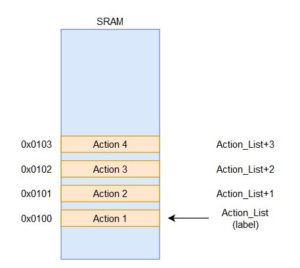 Action 1 is associated with the SRAM address 0x0100 and the name Action_List. Action 2 is linked to the SRAM address 0x0102 and can be referred to with the name Action_List+1. The rest can be extrapolated from there. In terms of the code that would be needed to load the data for all four actions, add 3 to the value, and store it back, it would look something like this.
ldi R16, 0x03                              ldi R16, 0x03
lds R17, Action_List                       lds R17, 0x0100
add R17, R16                               add R17, R16
sts Action_List, R17                       sts 0x0100, R17
lds R17, Action_List+1                     lds R17, 0x0101
add R17, R16                               add R17, R16
sts Action_List+1, R17          OR           sts 0x0101, R17
lds R17, Action_List+2                     lds R17, 0x0102
add R17, R16                               add R17, R16
sts Action_List+2, R17                       sts 0x0102, R17
lds R17, Action_List+3                     lds R17, 0x0103
add R17, R16                               add R17, R16
sts Action_List+3, R17                       sts 0x0103, R17
If a calculation or modification needs to be made to the action values, it would involve another set of 4 to 8 instructions. Overall, it could require a total of 12 or more instructions just to do one action on these variables. If you had to deal with a large number of variables within a loop that repeats a certain number of times, the code could get very unmanageable. This is why the direct addressing mode is suitable for small scale applications but becomes tedious for data processing applications that need to deal with hundreds of thousands of values in a data set.
On the other hand, indirect addressing is ideal for dynamically dealing with large sets of data and has no problem scaling as needed. The logic behind how the code needs to be structured is a little more complicated but it will reduce the number of instructions needed. The key detail is that the information about the location of the data is handled within a separate register that is referred to as a pointer. This register can be dynamically modified by the program, so that the location the indirect addressing instruction is using is different. Rather than having the address included within the instruction, the machine code encoding has a value representing which pointer register is being used. An example is shown in the figure below.
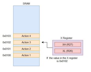 In this situation, we are still dealing with the SRAM variable called Action_List with a total of four actions. The same address values are used (from 0x0100 to 0x0103) but the way we refer to it has changed. Here, we have the X register which is our pointer to the location it will be dealing with. The X register is the register pair of R27 and R26, so whatever value is placed into those two registers will be the SRAM address the indirect addressing instruction uses. From the figure, if you wanted to work with Action 3, the value inside the X register has to be 0x0102. This may seem more involved to handle each value of the list but it allows us to do so much more.
The general structure of the program using indirect addressing will usually be something like the following.
1) Initialize pointer register to the start of the data table or variables to work with.
2) Load data if needed
3) Perform action on data
4) Modify pointer register if needed
5) Store data back if needed
This structure allows us to simplify the example from above into the following.
start:
    ldi R27, 0x01                   ldi XH, HIGH(Action_List)
    ldi R26, 0x00                   ldi XL, LOW(Action_List)
    ldi R16, 0x04                   ldi R16, 0x04
    ldi R17, 0x01                   ldi R17, 0x01
    clr R15                         clr R15
looping:
    ld R18, X                       ld R18, X
    add R18, R17        OR          add R18, R17
    st X, R18                       st X, R18
    add R26, R17                    add XL, R17
    adc R27, R15                    adc XH, R15
    dec R16                         dec R16
    brne looping                    brne looping
You should be able to identify which lines of code correspond to that structure. In this case, the X register is initialized to the start of Action_List. We also prepare the values to add 1 to the value of the action as well as how many times to loop for. From there, the value is loaded into R18 before adding 1 to it and storing it back. The X register is increased by 1 to move onto the next spot before the loop continues. On the second loop, it is now pointing to Action_List+1 or 0x0101 and performs the same action. In this situation, the number of lines of code is only one less than the previous example but it is significantly easier to scale up. If there were now 150 actions in the list, the direct addressing example would have a total of 450 instructions. For the indirect addressing mode, I would only need to change the number of times it would loop for and it would have a total of 12 instructions.
Now that we have covered the basic concept, we can go over some additional details that make more complex applications easier to program.
1) For indirect addressing within SRAM, there are a total of three pointer registers available. This allows you to theoretically be handling three separate locations at once if needed. Most of the time, it will be easier to reuse a single pointer once each location has been dealt with. The pointers are called the X, Y, and Z registers. X is the R27:R26 pair, Y is the R29:R28 pair, and Z is the R31:R30 pair.
2) LD is used to load the data from the location that is indicted by the pointer register. ST is used to store data to the location that is indicated by the pointer register.
3) Modifying the pointer register by 1 within a loop can be accomplished with pre-decrement or post-increment. Pre-decrement will subtract the pointer register by 1 before performing the specific action (load or store). Post-increment will perform the action and then increment afterwards. For example, the code above could be simplified into the following.
st X, R18
add XL, R17        Becomes ---->        st X+, R18
adc XH, R15
This can also be applied to LD as well. It is indicated by adding the sign to the pointer register used. So post-increment with LD would be LD R18, X+. If the value in the X register was 0x0100, the LD instruction would load the data from the SRAM address 0x0100 and then modify the X register to be 0x0101. For pre-decrement, it has a minus sign in front of the pointer register (LD R18, -X).
4) If the pointer register needs to be continually modified by a certain amount, you can utilize the indirect addressing with displacement instructions (LDD or STD). This is only applicable if you need to grab every third value from the data table or something similar. The instruction would look like this – LDD R18, Y+3.
Assigning Values to Actions for the Action List
With the background of using indirect addressing, we can now move onto assigning values to represent the different actions. This is our personal choice for how the robot will know what to do when it reads the information from the action list. There are four actions to handle (forward, turn left, turn right, and turn around). To make things simple, we can define these with specific values. Please add the following equate statements to your code. If you already have a label or subroutine with the same name as these equate statements, please change these names to avoid problems.
.EQU forward = 0x00
.EQU turn_left = 0x01
.EQU turn_right = 0x02
.EQU turn_around = 0x03
With this out of the way, you will now need to define the action list that you want to test. As there needs to be a minimum of 5 actions and it needs to call each action once, you might get something like the following – forward, turn_left, forward, turn_right, forward, turn_around. There are a total of six actions and it will make it easy to see what action the robot should be executing if there are any problems. You will need to define this new variable and initialize it with the appropriate values. It will look something like the following. Make sure to assign the appropriate number of bytes for your variable.
.DSEG
next_state: .BYTE 1
turning: .BYTE 1
action_list: .BYTE 6

// Other code //
reset:
// other code //
// Initialize values of action list
ldi R16, forward       // load value to represent forward
sts action_list, R16   // Save first forward action
ldi R16, turn_left     // load value to represent turn_left
sts action_list+1, R16 // Save second action
ldi R16, forward       // load value to represent forward
sts action_list+2, R16 // Save second forward action
ldi R16, turn_left     // load value to represent turn_right
sts action_list+3, R16 // Save fourth action
ldi R16, forward       // load value to represent forward
sts action_list+4, R16 // Save thrid forward action
ldi R16, turn_left     // load value to represent turn_right
sts action_list+5, R16 // Save sixth action
You may wonder why we have to save the values manually. Because the variable is in SRAM, it defaults to a value of zero. As we have a specific sequence that we want to test, we will need to initialize it ourselves. The benefit of this is that we can modify the sequence later on if the robot needs to execute a second sequence of actions. The alternative to this is to have the action list saved within flash program memory, which we will go over in the next lab.
Updating State 1 to execute the action list
Now that we have completed those parts, we can now finish updating state 1 to execute the appropriate action once the program has figured it out. As we will need to cycle through the action_list, we need to set up a looping structure and a way to keep track of which action it is currently executing. We also would like to have the robot repeating the sequence of actions, so it will need to reset once it has gone through the entire sequence.
As you may have guessed, State 1 will need to be completely re-written in order to implement this. The following list covers the major objectives that we need to take care of.
1) Load data from the action_list for the current action.
2) Determine which subroutine to call or the code to execute for said action
3) Update counter keeping track of the actions performed
4) Check to see if the end of the action_list has been reached. Restart back at the beginning of the sequence if so.
In order to load the data, we will use the knowledge about indirect addressing in order to implement this. Following that general structure, the code will look something like this in order to load the current action and prepare for the next one.
ld R16, X+      // Load data from current location pointed to by X and post-increment
                // to prepare for next action.
You may be wondering what happened to the initialization of the pointer register. Because State 1 will not be called continuously as the robot cycles between State 0 and State 1, we do not want to initialize the pointer register within State 1. This will cause us to keep pointing to the beginning of the action_list and it will never move to the second action. We can add more code to address this such as adding the counter to the pointer register but that can be avoided if we initialize it outside of State 1, such as within the reset section. It will look something like this.
reset:
// other code //
ldi XH, high(action_list)
ldi XL, low(action_list)

// other code //

loop:
// other code //

state_1:
    ld R16, X+    // Load data from current location pointed to by X and post-increment
                  // to prepare for next action.
By doing it this way, we will always start at the beginning of the sequence and it will proceed one action at a time. One thing to be aware of is that we need to make sure that there are no other lines of code that will modify R27:R26 as that will disrupt this structure. With that out of the way, we can move onto the next objective. In order to determine which action to execute, we can use the typical comparison and branch structure. Here, you are just verifying what the value loaded into R16 matches. If it is to go forward, we can handle this action by having it go back to line following. This will get the robot to move forward until it hits the next intersection, where the next action is to be done. That means we do not need to call any subroutines and just need to go back to State 0. You SHOULD NOT jump to the state right away. We will handle it like the timer 1 ISR, where we update the next_state variable to be equal to S0 and then move to the end of state 1. For the turning actions, you will need to call the appropriate subroutines to turn and the robot should move forward to the next room. The code should look something like this.
state_1:
     ld R16, X+ // Load data from current location pointed to by X and post-increment
                // to prepare for next action.
     cpi R16, forward
     breq forward_step
     cpi R16, turn_left
     breq left_step
     cpi R16, turn_right
     breq right_step
around_step:
     rcall turning_around
     rjmp end_s1
forward_step:
     rjmp end_s1
left_step:
     rcall turning_left
     rjmp end_s1
right_step:
     rcall turning_right
end_s1:
     ldi R17, S0
     sts next_state, R17
     rjmp endLoop
The next step after this is to incorporate a counter to keep track of when to restart the sequence of actions. Define another SRAM variable called action_count and initialize it to 1. We will add this to the end of state 1, where it will be incremented by 1 after executing the action. Given there are only six actions, we know what the value to compare to should be when the restart is to occur. The code will look like the following.
end_s1:
     ldi R17, S0
     sts next_state, R17
     lds R18, action_count
     inc R18
     sts action_count, R18
     cpi R18, 0x07
     brne skip
     ldi XH, high(action_list)
     ldi XL, low(action_list)
     ldi R19, 0x01
     sts action_count, R19
skip:
    rjmp endLoop
That should be everything you need for this lab.
Lab 5 Deliverable(s)
|
All labs should represent your own work – DO NOT COPY. Submit your list file as defined below. Make sure that the code compiles without any errors. Do not forget to comment your code. Lab 5 Demonstration
|
Assembly Robot Prelab 6 – Indirect Addressing (SRAM)
Table of Contents
Introduction
The focus of this prelab is to provide you with additional practice with indirect addressing and how it will be used in the labs. We also go over some of the more advanced ways it can be used.
Indirect Addressing
First, we need to review the difference between the direct addressing mode and indirect addressing. For the direct addressing mode (LDS, STS, IN, OUT, etc), the location of the data is fixed. It must be specified directly and is a part of the machine code encoding. This is to provide the CPU with the information that it needs. Because of this, each instruction to load or save to a variable or set of variables is unique. If you need to cycle through the variables as part of a loop, it will require one or more line of code per variable. This can result in pretty lengthy code depending on the implementation. For example, let us say we are working with an SRAM variable called Action_List that is 4 bytes large. Each individual action will be stored at each byte, so we have a total of 4 actions. The way that we can refer to each location is depicted below.
 Action 1 is associated with the SRAM address 0x0100 and the name Action_List. Action 2 is linked to the SRAM address 0x0102 and can be referred to with the name Action_List+1. The rest can be extrapolated from there. In terms of the code that would be needed to load the data for all four actions, it would look something like this.
ldi R16, 0x03                              ldi R16, 0x03
lds R17, Action_List                       lds R17, 0x0100
add R17, R16                               add R17, R16
sts Action_List, R17                       sts 0x0100, R17
lds R17, Action_List+1                     lds R17, 0x0101
add R17, R16                               add R17, R16
sts Action_List, R17          OR           sts 0x0101, R17
lds R17, Action_List+2                     lds R17, 0x0102
add R17, R16                               add R17, R16
sts Action_List, R17                       sts 0x0102, R17
lds R17, Action_List+3                     lds R17, 0x0103
add R17, R16                               add R17, R16
sts Action_List, R17                       sts 0x0103, R17
If a calculation or modification needs to be made to the action values, it would involve another set of 4 to 8 instructions. Overall, it could require a total of 12 or more instructions just to do one action on these variables. If you had to deal with a large number of variables within a loop that repeats a certain number of times, the code could get very unmanageable. This is why the direct addressing mode is suitable for small scale applications but becomes tedious for data processing applications that need to deal with hundreds of thousands of values in a data set.
On the other hand, indirect addressing is ideal for dynamically dealing with large sets of data and has no problem scaling as needed. The logic behind how the code needs to be structured is a little more complicated but it will reduce the number of instructions needed. The key detail is that the information about the location of the data is handled within a separate register that is referred to as a pointer. This register can be dynamically modified by the program, so that the location the indirect addressing instruction is using is different. Rather than having the address included within the instruction, the machine code encoding has a value representing which pointer register is being used. An example is shown in the figure below.
 In this situation, we are still dealing with the SRAM variable called Action_List with a total of four actions. The same address values are used (from 0x0100 to 0x0103) but the way we refer to it has changed. Here, we have the X register which is our pointer to the location it will be dealing with. The X register is the register pair of R27 and R26, so whatever value is placed into those two registers will be the SRAM address the indirect addressing instruction uses. From the figure, if you wanted to work with Action 3, the value inside the X register has to be 0x0102. This may seem more involved to handle each value of the list but it allows us to do so much more.
The general structure of the program using indirect addressing will usually be something like the following.
1) Initialize pointer register to the start of the data table or variables to work with.
2) Load data if needed
3) Perform action on data
4) Modify pointer register if needed
5) Store data back if needed
This structure allows us to simplify the example from above into the following.
start:
    ldi R27, 0x01                   ldi XH, HIGH(Action_List)
    ldi R26, 0x00                   ldi XL, LOW(Action_List)
    ldi R16, 0x04                   ldi R16, 0x04
    ldi R17, 0x01                   ldi R17, 0x01
    clr R15                         clr R15
looping:
    ld R18, X                       ld R18, X
    add R18, R17        OR          add R18, R17
    st X, R18                       st X, R18
    add R26, R17                    add XL, R17
    adc R27, R15                    adc XH, R15
    dec R16                         dec R16
    brne looping                    brne looping
You should be able to identify which lines of code correspond to that structure. In this case, the X register is initialized to the start of Action_List. We also prepare the values to add 1 to the value of the action as well as how many times to loop for. From there, the value is loaded into R18 before adding 1 to it and storing it back. The X register is increased by 1 to move onto the next spot before the loop continues. On the second loop, it is now pointing to Action_List+1 or 0x0101 and performs the same action. In this situation, the number of lines of code is only one less than the previous example but it is significantly easier to scale up. If there were now 150 actions in the list, the direct addressing example would have a total of 450 instructions. For the indirect addressing mode, I would only need to change the number of times it would loop for and it would have a total of 12 instructions.
Now that we have covered the basic concept, we can go over some additional details that make more complex applications easier to program.
1) For indirect addressing within SRAM, there are a total of three pointer registers available. This allows you to theoretically be handling three separate locations at once if needed. Most of the time, it will be easier to reuse a single pointer once each location has been dealt with. The pointers are called the X, Y, and Z registers. X is the R27:R26 pair, Y is the R29:R28 pair, and Z is the R31:R30 pair.
2) LD is used to load the data from the location that is indicted by the pointer register. ST is used to store data to the location that is indicated by the pointer register.
3) Modifying the pointer register by 1 within a loop can be accomplished with pre-decrement or post-increment. Pre-decrement will subtract the pointer register by 1 before performing the specific action (load or store). Post-increment will perform the action and then increment afterwards. For example, the code above could be simplified into the following.
st X, R18
add XL, R17        Becomes ---->        st X+, R18
adc XH, R15
This can also be applied to LD as well. It is indicated by adding the sign to the pointer register used. So post-increment with LD would be LD R18, X+. If the value in the X register was 0x0100, the LD instruction would load the data from the SRAM address 0x0100 and then modify the X register to be 0x0101. For pre-decrement, it has a minus sign in front of the pointer register (LD R18, -X).
4) If the pointer register needs to be continually modified by a certain amount, you can utilize the indirect addressing with displacement instructions (LDD or STD). This is only applicable if you need to grab every third value from the data table or something similar. The instruction would look like this – LDD R18, Y+3.
Questions
Question 1 – Assume that an SRAM variable called voltage_data is defined and is initialized. This variable is assigned to the address 0x0104 and has 15 bytes allocated for the data. Using the following code, what is the value within the pointer register after it is executed?
ldi ZH, high(voltage_data+6)
ldi ZL, low(voltage_data+6)
Question 2 – After those lines of code have been executed, our program needs to access the data from the twelfth byte of the variable. Write the code that will modify the pointer register to point at the proper location. Make sure to load the constant that is going to be used into a separate register.
Question 3 – Explain what the following piece of code will do. Cover details such as how many times the code will repeat, how the data is accessed, what is being done to the data, and so on.
ldi YH, high(voltage_data)
ldi YL, low(voltage_data)
ldi R16, 0x1C
ldi R17, 0x05
loop:
    ld R18, Y
    add R18, R17
    st Y+, R18
    dec R16
    brne loop
Question 4 – Assume that the SRAM variable test has been defined and has the following values initialized (0x03, 0x08, 0xA8, 0xF3, and 0x97). Once the following code has been executed, what value will be loaded into R17?
ldi ZH, high(test)
ldi ZL, low(test)
ldi R16, 0x03
clr R18
add ZL, R16
adc ZH, R18
LD R17, Z
Prelab 6 Deliverable(s)
Page 1 – Title Page with Name, lab title, and photo
Page 2 – Answers to questions
Assembly Robot Prelab 7 – Indirect Addressing (FLASH)
Introduction
The focus of this prelab is to help you understand the difference between indirect addressing with FLASH and indirect addressing with SRAM. These problems will also reinforce the base address + index concept as well as provide a few examples of the code structure.
Questions
1) What value is being loaded into the Z register based on the code given below? Assume the data table called measurement starts at 0x0148.
ldi ZH, high(measurement<<1)
ldi ZL, low(measurement<<1)
2) Write the code that will define the data table called output that has the following values stored: 0xA8, 0x83, 0x19, 0xE2, 0x6F. Make sure it is located at the address 0x018D in FLASH.
3) Using the information defined in problem 2, what value will be loaded into register 19 if the following code is executed?
ldi ZH, high(output<<1)
ldi ZL, low(output<<1)
ldi R18, 0x03
clr R19
add ZL, R18
adc ZH, R19
lpm R19, Z
4) Explain the purpose of the Z pointer register in regards to indirect addressing with FLASH. How is it different from the pointer registers used in indirect addressing with SRAM?
Prelab 7 Deliverable(s)
Page 1 – Title Page with Name, lab title, and photo
Page 2 – Answers to questions and completed tables

