Microcontroller Based Interface Design
Part 1
System Engineering Your Robot
Table of Contents [hide]
Introduction
In this post I am going to talk about the 3DoT Microcontroller Board and its integration with peripheral devices including sensors, actuators, and serial communications. A basic knowledge of programming in C++ is assumed.
Microcontroller Based Interface Design
Embedded Systems
Engineers design systems. A system can be characterized by a box with an input and output. Typically the engineer is tasked to design the box with a given set of inputs and the desired output.
- When a controller “the brain” is part of the design solution, the design is known as an Embedded System.
- The controller may be implemented using an ASIC (Application Integrated Circuit), FPGA (Field Programmable Gate Array), or in most cases a Microcontroller. A combination of the above on a single IC, is known as a System on a Chip (SoC).
- For this discussion, the input device is by definition a Sensor, and the output device an Actuator.
In this post we look at the microcontroller based system design used by our robots. It is hoped that by looking at this specific example you will be able to apply the lessons learned to the design of other microcontroller-based systems.
Robot Microcontroller Based System Design
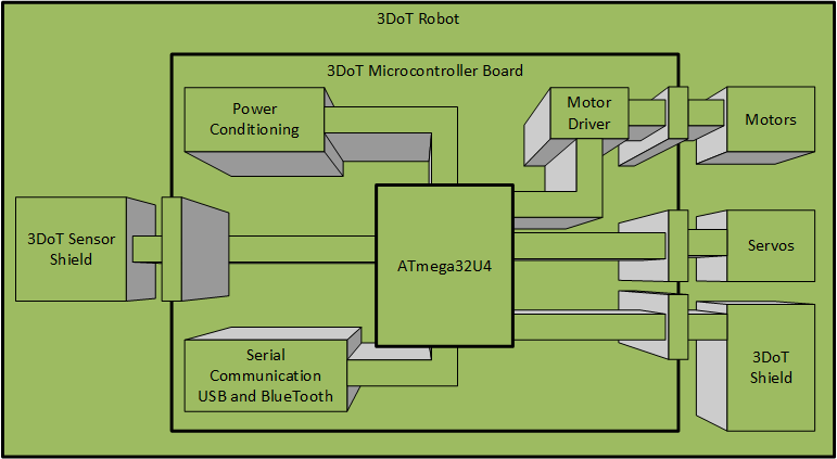
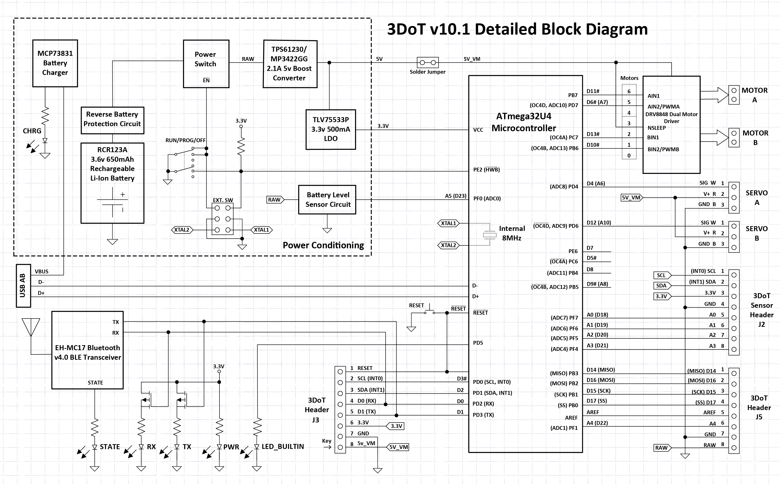
Figure 2.0 illustrates our robot design from a generic capabilities perspective. At the heart of our embedded system is an ATmega32U4 Microcontroller.
The ATmega32U4 is built into the Arduino compatible 3DoT (3D of Things) Board. Let’s take a closer look at the hardware and software built into the 3DoT board.
Hardware
The 3DoT board is a micro-footprint 3.5 x 7 cm all-in-one Arduino compatible microcontroller board, that integrates all the components needed to create a small autonomous, RC controlled, or telepresent robot.
- Microcontroller: At the heart of the 3DoT board is an Arduino Leonardo based microcontroller unit (ATmega32U4), featuring an 8 MIPS (Millions of Instructions Per Second) 2-stage pipelined AVR RISC processor.
- USB (Universal Serial Bus) serial communications circuitry allows you to upload your programs and download data.
- An FCC-certified BLE 5.0 module (optional) allows wireless communication with the ArxRobot Android/iPhone App and Arxterra control panel.
- Power Management: Power for the 3DoT board is provided by an RCR123A LiPo 650 mAh rechargeable battery with associated power protection, switching, and conditioning circuitry (3.3v and 5v). Plus, an integrated 3.7v Li-ion battery charger with battery level sensor circuit. You also have access to an external battery connector – for input voltages between 4 – 18 V.
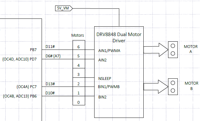
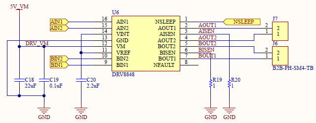
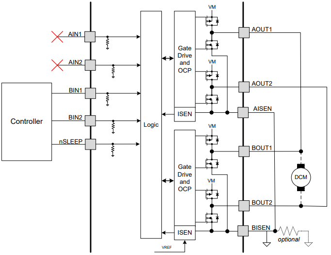
- Motors & Servos: To control your robot’s motors the 3DoT board includes a DRV8848 Dual Motor Driver. JST Connectors are provided for up to two (2) DC Motors and two (2) Micro or Ultra-Micro Servos.
- Expansion: Customize your robot with 8-pin forward sensor and 16-pin 3DoT Shields, also known as daughter boards.
- 16-pin top female headers for shields – providing I/O, I²C, SPI, USART, 3.3 V and 5 V.
- The forward-facing 8-pin female header for sensor shields – providing 4 analog pins, I²C, and 3.3 V power – for sensor shields like infrared or metal-detecting shields. Great location for headlights, lasers, ultrasonics, etc.
- Programming switch: Three-position switch for easy programming
- No more double-tapping a button and rushing to program your board, or your robot trying to drive away while programming. Set the switch to PRG to program, RUN to execute your code.
Software
- Programs are written in the Arduino IDE (Integrated Development Environment).
- Pre-installed Arxterra 3DoT bootloader plus Robot3DoTBoard library – fully customizable for your robot
- Together this software suite running on the ATmega 32U4 microcontroller allows you to control a 2-wheel robot out-of-the-box using the FREE ArxRobot Android/iPhone App.
- If the robot can hold your phone, then you can remotely control your robot from anywhere with an internet connection from the Arxterra Control Panel.
Document Objective
The objective of this document is to teach you how to interface peripheral devices to a microcontroller based system. We first…
- Allocating the resource of our MCU (Micro-Controller Unit).
- Look at how sensors and actuators could be incorporated into this design
- Present the reference design as an example.
Allocating MCU Resources
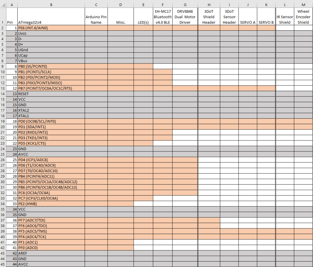
Our embedded system is comprised of a 3DoT Microcontroller Board. At the heart of the system is the ATmega32U4 microcontroller. The 3DoT board consumes some of the resources of the ATmega32U4 in exchange for extending the capabilities of the integrated system. Table 1 provides a mapping of these resources and ultimately the interface resources available to the sensors and actuators of your robot in columns G through K. Columns L and M show how the 16-pin 3DoT and 8-pin sensor headers can be used to add an IR sensor and wheel encoder shields.
ATmega32U4 I/O pins (columns A and B)
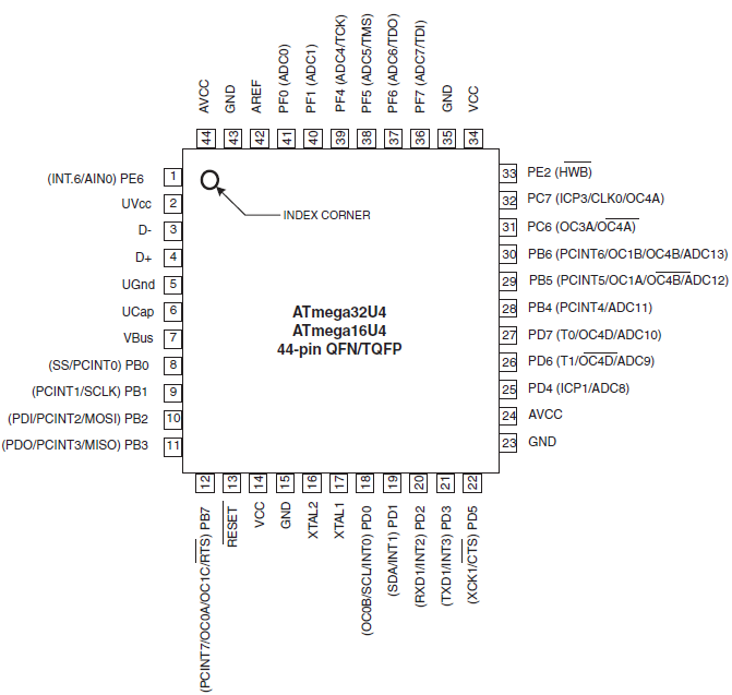
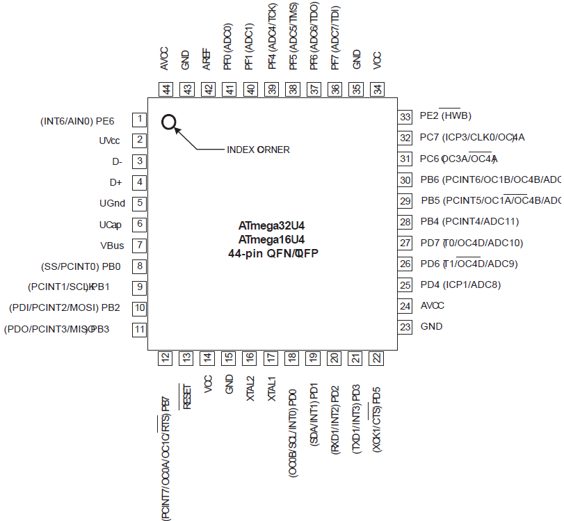
The ATmega32U4 comes in a 44-pin QFN (Quad Flat No-leads) and a TQFP (Thin Quad Flat Package). The arrangement of these pins around the QFN or TQFP IC is shown in Figure 3.0. Each pin is assigned both a number and a name.
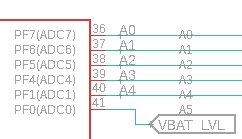
Due to pin-out limitations of the IC package (QFN and TQFP), most I/O pins of the ATmega32U4 are multiplexed. Specifically, they can be programmed to provide different interfaces to the system. For example, pin 41 PF0 (ADC0) can be wired to a digital I/O device like a button or and LED. Conversely it could be wired to an analog input to measure a voltage output by an IR sensor.
Figure 3.0 ATmega32U4 Pin-out
Table 3.0 allows us to place the ATmega32U4 within the context of our design. Specifically, how are we going to wire up all the actuators and sensors to our microcontroller IC. We begin by adding each pin number and its name to columns 1 and 2 respectively.
As shown in Table 3.0 most but not all rows may be assigned as I/O pins. For example the VCC, GND, USB, XTAL (crystal) and reset pins are not available. These non-I/O pins appear as Gray rows in the table. What this means to the system designer instead of having 44 Multiplexed I/O pins you now only has twenty twenty-six (26). All 26 of these multiplexed pins may be used as digital I/O pins (PB7-0,PC7-6,PD7-0,PE6 and PE2, PF7-4 and PF1-0). These I/O pins appear as Orange rows in the table. When one of these I/O pins is consumed, the remainder of the row is White.
Arduino I/O Pins (column C)
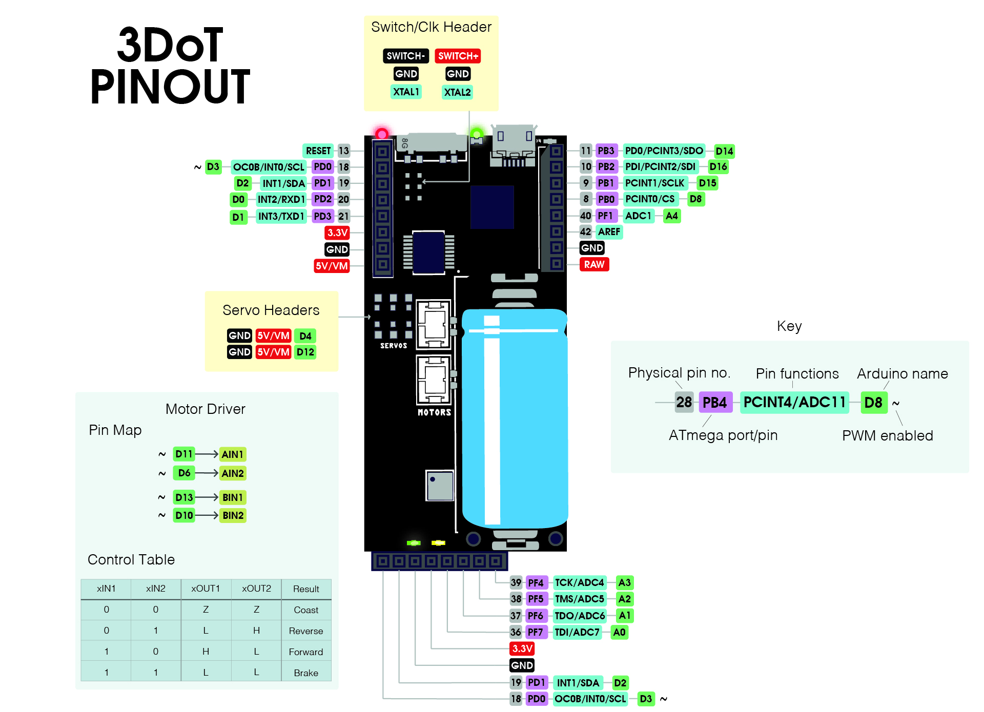
The Arduino was designed as a tool for introducing students to embedded systems. To a student unfamiliar with peripheral subsystems like GPIO (General Purpose Input Output) ports and an ADC (Analog to Digital Converter), the names assigned to the pins of the ATmega32U4 can be intimidating. Instead, the creators of the Arduino realized that these complex electronic systems could be introduced in a step-by-step fashion by starting with the function to be performed. Put another way, students new to engineering are more interested in “what” the pin can do, rather than “how” it does it. For this reason, the Arduino creators renamed the pins by function. For example, pins that work with digital binary inputs and outputs start with the letter D and are numbered sequentially (D0 to D23). Pins that work with Analog inputs start with the letter A and are again numbered sequentially (A0 – A10). Along with these “functional” names came simple program instructions, like digitalRead(D0) and digitalWrite(D1) for digital signals and analogRead(A0) for analog inputs.
The 3DoT instruction set builds on this functional vs. technical philosophy by allowing you to control your robot’s movements with a single move() instruction.
Table 1.0 Column C shows the Arduino names assigned to each ATmega32U4 I/O pin (orange rows). Specifically, digital pins D0 to D23 and analog inputs A0 to A11. The single exception is pin 33 PE2 (HWB) which is set to 0 (wired to ground) for Arduino ATmega32U4 microcontroller boards. The 3DoT board wires this pin to its ON/PROG/RUN switch. This change was made to make the 3DoT board easier to program than its Arduino cousins.
3DoT
To build an Arduino-based telerobotic Robot, in addition to the microcontroller board you would need a battery, charger, Bluetooth shield, motor shield, and a breadboard containing miscellaneous parts. The 3DoT board integrates all these components on a single 3.5 cm x 7 cm board. As a part of your robot, all these built-in functions consume microcontroller pin resources as defined in columns D, E, and F. In most instances, once used these resources are no longer available to implement other functions.
DRV8848 Motor Driver (column F)
Figure 3.1 shows how the DRV8848 Dual Motor Driver is wired to a typical MCU. Looking at Table 3.0 column F we see that our motor driver is wired to pins pin 25 to 31 of the ATmega32U4 MCU. Also notice that after this column these rows are colored white indicating that the resources are no longer available to the system.
EH-MC17 Bluetooth Module (column E)
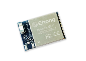
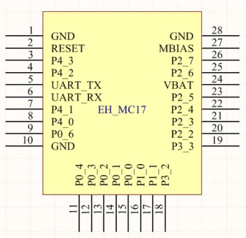
The EH-MC17 (Figure 7) sends and receives data to the USART peripheral subsystem of the MCU. The USART serial interface only needs 2 wires (RX and TX) to physically implement this interface. As shown in column B of Table 3.0 the TX1 and RX1 pins are internally routed from the USART peripheral subsystem to pins 20 and 21 of the ATmega32U4 IC. A few additional things are of note here.
- To add this Bluetooth module we need to sacrifice Arduino digital pins D0 and D1.
- Unlike the motor driver, these two rows do not immediately show these pin resources as being consumed. Specifically, they are brought out to the 3DoT Shield Header J1 (column G). The reason is simple. The addition of the HM-11 module to the 3DoT board is optional. If the robot designer chooses to not solder the HM-11 module to the bottom of the 3DoT board, then they are free to use these pins to implement a different serial communication standard (e.g. XBee, WiFi) or for a fully autonomous robot, Arduino digital pins Do and D1 are again available.
- It is curious to note that the MCU d0/RX1 pin is wired to the HM-11 TX pin and that the MCU d1/TX1 pin is wired to the HM-11 RX pin. Confusing isn’t it and also a very common wiring error. You can think of it this way; one person’s output is another person’s input.
LEDs, Switch, and Battery Level Circuit (column D)
Beyond the Motor Driver (Table 3.0 column F) and the HM-11 Bluetooth module (Table 3.0 column E) the 3DoT Board uses a few additional MCU pin resources for LEDs (Light Emitting Diodes), the ON/PROG/OFF Switch, and the Battery Level circuit. Let’s take a closer look at column D of Figure 3.0.
LEDs
RX LED 4 and TX LED 6 are wired to pin 8 (Arduino pin D17/RXLED) and pin 22 (Arduino pin TXLED). The famous Arduino on-board LED typically uses by the BLINK script, is wired to pin Port D bit 5, not Arduino digital pin 13.
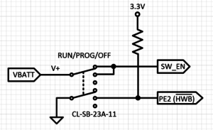
DP3T OFF/PROG/RUN Switch
The Arduino Leonardo and in fact all Arduino 32U4 based boards have a peculiar problem as a result of the ATmega32U4 incorporating the USB peripheral system as part of the MCU. On “traditional” Arduino boards, like the UNO, a separate ATmega MCU is dedicated to implementing the USB interface. As a result, ATmega32U4 based Arduinos must juggle between the user uploading programs and acting as a USB port for the user’s program. You need the first function when you are programming and the second if you want your program to interface to the computer. For example, if you want your program to output to the Arduino IDE’s Serial Monitor. The Arduino developers solved this problem by having the Arduino upon reset look for the user to upload a program and after a few seconds, if the user does not start the upload process then it switches to running the currently loaded program. In many cases, the user can not initiate this upload process fast enough for the Arduino’s liking resulting in the “double-tap” solution which only works part of the time. To solve this problem 3DoT developers implemented a different solution. The 3DoT board has a DP3T (Double Pole Triple Throw) Switch. As the name implies this switch has three positions (OFF/PROG/RUN). Now the ATmega32U4 bootloader, by interrogating pin Pin 33 PE2 (HWB), can directly determine if you want to upload a program (PROG) to the ATmega32U4 or RUN your program.
Battery Level Circuit
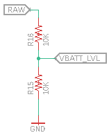
Going back to Table 3.0 column D row/pin 41 we see VBATT_LVL. Which is short for “Voltage Battery Level.” As the name implies the function of this pin is to read the current battery voltage. A simple voltage divider is all it takes to implement the battery level circuit, with the top of the voltage divider wired to the positive lead of the battery and the center of the divider wired to pin 41. The output of this circuit is an analog voltage typically between 2.1 and 1.2 volts. Going back to pin 41 we see that the ATmega32U4 names this pin PF0 (ADC0), while the Arduino names the pin A5/D23. The key here is that the pin can be both an analog input or digital input or output. So to implement this function, we will be using the Analog to Digital (ADC) peripheral subsystem of the ATmega32U4 and not the General Purpose I/O (GPIO) port used for digital inputs and outputs.
Robot
In this section we are going to look at the MCU resources available for customizing your robot. As already mentioned the 3DoT board directly supports a robot with two (2) DC motors and two (2) micro-servos. The DC motors are controlled by the TB6612FNG motor driver IC whose pins have already been allocated. The micro-servos have their own dedicated connector J7 (Figure 4.1), and wire directly to the ATmega32U4 through limiting resistors. The limiting resistors protect the MCU from damage in the event of an accidental short for the V7 boards.
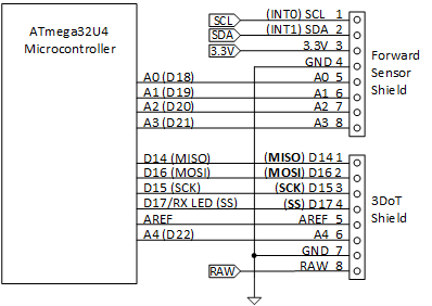
Customization of your robot is afforded by three 8-pin connectors J1, J2, and J3. Daughter boards that plug into connectors J1 and J2 will be called “3DoT Shields.” Daughter boards that plug into connector J3 will be called “3DoT Sensor Shields.”
3DoT Shields
Connectors J1 and J2 are located on the top of the board in a fashion similar to the Arduino UNO, and like the UNO can support one or more stackable 3DoT Shields. This is especially true of the 3DoT board, whose J1 and J2 connectors support three (3) different serial communication protocols: I2C, SPI, and USART. To take this to the extreme, you could theoretically stack 127 I2C shields without even mentioning SPI and USART shields. In addition, the J2 pins 5 and 6 support one (1) Analog signal with an associated reference voltage (AREF). To avoid conflicts with 3DoT Sensor Shield (connectors J3) on the bottom of the board, do not wire digital I/O to I2C pins SDA and SDL (D2, D3). In addition, if your robot comes with the HM-11 Bluetooth module do not wire digital I/O to USART pins RX and TX (D0, D1).
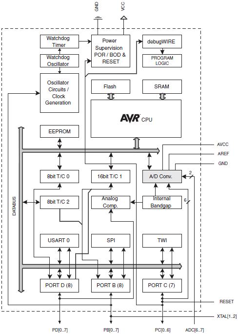
As we have seen, the multiplexing of the I/O pins immediately forces the system engineer to make trade-offs in the design of their shields. For example, If your making a fully autonomous robot (no HM-11 Bluetooth module), you do not need the single analog input A4 on connector J2, and are your forward 3DoT sensor shield is not using I2C pins SDA and SCL, then your 3DoT Shield could have a maximum of nine (9) digital I/O signals. In most designs all those conditions will not be met, and you will have to trade-off one MCU peripheral subsystem (see Figure 4.2) against another (GPIO Port, A/D Converter, I2C, SPI, and USART).
3DoT Sensor Shields
Connector J3 is an 8-pin connector located on the front bottom of the board. This connector is designed for “sensor shields” located on the front of the robot. Typical applications would include line following robots. With sensors in mind, the connector includes four analog inputs (A0 to A3) and support for the I2C serial communication protocol (SCL, SDA). For sensor shields requiring digital I/O lines it is recommended that one or more of the analog pins (D18 to D21) be utilized. As mentioned in the previous paragraph, to avoid conflicts with 3DoT Shields (connectors J1 and J2) on the top of the board, do not wire digital I/O to the I2C pins (D2, D3).
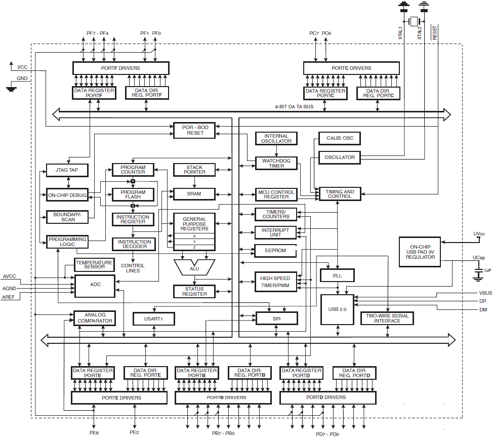
Figure 4.2 ATmega328P Block Diagram
| In the future when I talk about Arduino peripheral subsystems, as I did in the previous paragraph, I will show the ATmega328P Block Diagram in place of the ATmega32U4 processor used on the 3DoT board. The ATmega328P microcontroller was used on the original Arduino UNO and is far simpler than the ATmega32U4. Therefore, I can make the same points using the ATmega328P, without adding unnecessary complexity to the topic under discussion. |
Next Step
Applying what you learned here, in “Microcontroller Based Interface” Design Part 2 we will look at how sensors and actuators can be incorporated into your robot.
Lecture 2 – Robot Sensors and Actuators
System Engineering Your Robot
Table of Contents [hide]
Interfacing Sensors and Actuators
Reading
- Microcontroller Interfacing Circuits by Revolution Education Ltd.
- For help with a specific interface, or just to look for ideas, visit the related Arduino Forum.
- A detailed discussion of Pulse Width Modulation is beyond the scope of the document. We will be covering PWM in more detail later in the semester. For now you may want to read this nicely illustrated article: Working with Atmel AVR Microcontroller Basic Pulse Width Modulation (PWM) Peripheral
Introduction
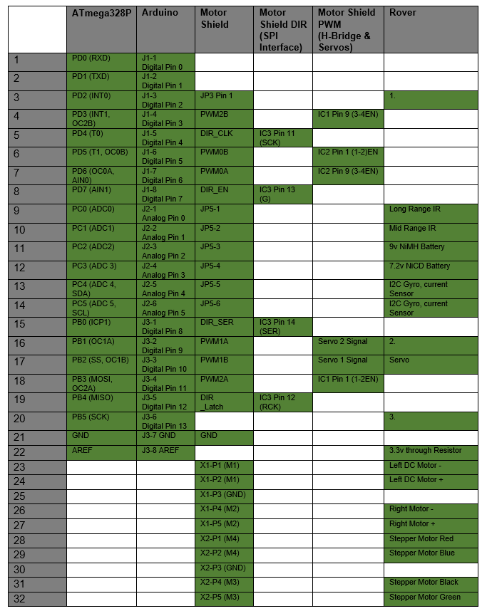
In Part 1 we developed a Resource Map for our rover (Table 1.0). In this section we look at how sensors and actuators could be incorporated into the design of our rover. Specifically, we will map our sensors and actuators to our I/O pins.
 Table 1.0 Rover Resource Summary
While Part 1 of this System Interface Design discussion was from the perspective of the ATmega328P; Part 2 will be presented from the perspective of the I/O device.
A detailed discussion of the ATmega328P subsystems, along with the software required to run them, is outside the scope of this document and will be covered in future lectures (hopefully).
Sensors
Digital Interface
Design Example: DIP Switch
A DIP switch is an example of a digital sensor which you could add to your design. For example to allow your robot to discover its mode of operation upon reset.
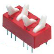
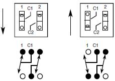
If you are not planning to implement the SPI interface and you do not have any Analog inputs, then working from the schematic of the device and the interface matrix, I would recommend wiring the four (4) Single Pole Double Throw (SPDT) DIP switch, shown in 1.0, to GPIO Pins (PF1, PB1, PB3, PB2, and PB1) of the ATmega32U4 or in Arduino parlance digital pins D22, D14, D16, D15. Button resources (Figure 2.1) would be allocated in a similar fashion.
Figure 1.0 Two SPDT DIP Switches
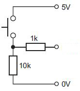
Figure 1.1 SPST Button Schematic
Parallel Interface
For our robots we are limited to no more than 9 digital inputs (see Section “3DoT Shields” in Part 1 of this series). Consequently, while wiring 1 button to the ATmega32U4 is not a problem, wiring a parallel device with a large word size is not directly possible. For example an 8-bit A/D converter would consume 89% of our available I/O resources. A much better solution would be an A/D converter that supports the I2C interface. Here we could get a 12-bit A/D converter with no loss in pin count.
Analog Interface
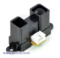
Many sensors output an analog voltage, including our IR sensors. The ATmega32U4 has a single ADC subsystem whose input can come from up to 6 multiplexed channels (ADC0 to ADC5). The reference design preserves all 6 of these analog channels. From a practical standpoint, the term multiplexed means that although our design can support up to 6 analog sensors, we can only read one at a time.
Design Example
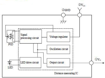
As with all devices, start with a schematic
Figure 2.3 Medium Range IR Sensor Block Diagram
From the block diagram it is seen that the interface of an IR sensor is a single analog wire. In the absence of any other resource requirements, we are free to wire this sensor output to any one of our six analog inputs (ADC0 to ADC5).
Voltage Range and Electromagnetic Interference (EMI)
When working with any analog interface you should be sensitive to the output swing of the analog signal and to the introduction of noise.
For our medium range IR sensor, the Voltage Output peaks at around 3.1 V. That means to maximize our resolution we will want to use an external voltage reference of 3.3V. The full scale reading of the ADC can be set to the AVCC (5 v), AREF, or an internal 1.1v reference voltage. So in this case we will want to wire a 3.3v reference source to AREF. In a future lecture you will also find we need to place a limiting resistor between the our reference source and AREF.
Noise is almost always a concern when working with an analog signal. For our IR sensor the data sheet recommends a 10 uF capacitor be placed as closely as possible to the sensor. In addition, analog signals are often sent over a twisted and shielded cable.
Actuators
Digital Interface
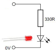
All ten available General Purpose I/O (GPIO) pins may be configured as outputs. The output circuit of the ATmega328 can sink or source a respectable 20 mA. This means that the ATmega328P can directly turn on/off LED indicators, without the need for an external driver (you will still need a limiting resistor).
Figure 3.0 Diode Circuit
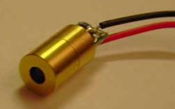
Another, digital actuator is our 650nm 1mW 8x13mm Laser Module. Once again before you purchase a device, make sure you have a datasheet. In the case of an laser, you need to know if it includes a current source, in which case you only need to turn the laser on/off, Otherwise, you will need to design in your own current source..
Figure 3.1 Laser Diode constant Current Circuit (source: Sparkfun Forum)
Motor and Pulse Width Modulation (PWM ) Interface
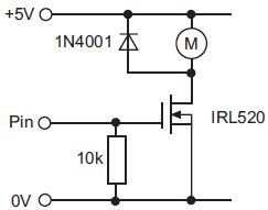
Motor On/Off
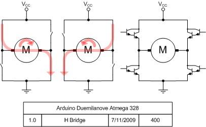
Change Motor Direction
Change the Speed of a Motor
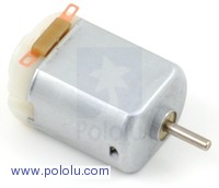
A simple variable resistor is all you need if you want to control the speed of a DC motor manually. To control the speed of a DC motor with a microcontroller you will use one of our six PWM channels (e.g., PWM1A, PWM1B).
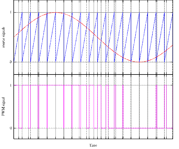
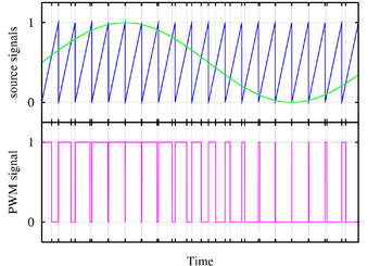
Figure 3.4 A simple method to generate the PWM pulse train corresponding to a given signal is the intersective PWM: the signal (here the red sinewave) is compared with a sawtooth waveform (blue). When the latter is less than the former, the PWM signal (magenta) is in high state (1). Otherwise it is in the low state (0).: Wikipedia
All the Above
If you want to turn your DC motor on/off, change direction, and control the speed of the motor you will need two (2) GPIO pins to configure the H-Bridge and a single PWM channel to control the speed. Without the Adafruit motor shield, If you wanted to control 4 DC motors (or 2 DC motors and a Bi-polar stepper motor) you would need eight (8) GPIO pins plus 4 PWM channels. With the motor shield we only lost 4 GPIO pins – we still need 4 PWM channels.
Attaching a DC motor to the Adafruit motor shield is as simple as wiring your DC motor to one of the four (4) Motor control connector pairs.
Servos
Reprinted from : Microcontroller Interfacing Circuits by Revolution Education Ltd.
A typical servo has just three connection wires, normally red, black and white (or yellow). The red wire is the 5V supply, the black wire is the 0V supply, and the white (or yellow) wire is for the positioning signal. The positioning signal is a pulse between 0.75 and 2.25 milliseconds (ms) long, repeated about every 18 ms (so there are roughly 50 pulses per second). With a 0.75ms pulse the servo moves to one end of its range, and with a 2.25ms pulse the servo moves to the other. Therefore, with a 1.5 ms pulse, the servo will move to the central position. If the pulses are stopped the servo will move freely to any position. Unfortunately servos require a large current (up to 1A) and also introduce a large amount of noise on the power rail. Therefore as with all motors, the servo should be powered from a separate power supply. Remember that when using two power supplies the two ground rails must be joined to provide a common reference point.
Serial Interface
The ATmega328P supports three serial interface protocols: Universal Asynchronous Receiver/Transmitter (USART), Serial Peripheral Interface (SPI), and Inter-Integrated Circuit (I2C). All three support two-way communications. This means that all three serial subsystems of the ATmega328P can work as easily with actuators as sensors (see Section 2.1) which implement one or more of these interface types.
Universal Asynchronous Receiver/Transmitter (USART)
For the purposes of this study, the USART will be reserved for communications between the rover and the PC. As we learned in Part 1, the USART subsystem uses two IC pins (TXD and RXD).
Serial Peripheral Interface (SPI)
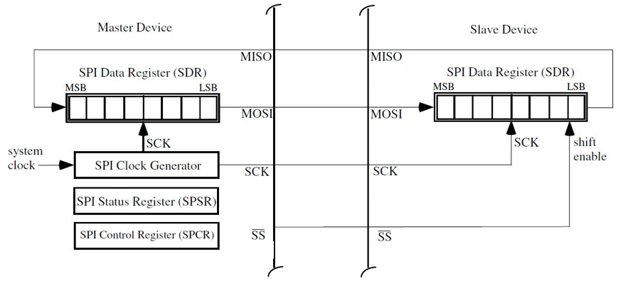
The SPI Subsystem of the ATmega328P requires four pins to implement 2-way serial communications (SCK, MISO, MOSI, SS). These lines are are wired to pins PB5 (SCK/PCINT5), PB4 (MISO/PCINT4), PB3 (MOSI/OC2A/PCINT3), and PB2 (SS/OC1B/PCINT2). Of interest here are Output Compare signals OC2A and OC1B. These signals are from the 8-bit Timer 2 and 16-bit Timer 1 subsystems. Both timer subsystems are used by the Adafruit motor shield to generate Pulse Width Modulated signals PWM2A and PWM1B. Pulse Width Modulation is critical for controlling the speed of DC motors (PWM2A) and setting the angle of a servo (PWM1B). Consequently, Adafruit implemented their SPI interface with General Purpose I/O (GPIO) ports and software. In this way they were able to maximize the number of PWM signals available to the shield, while sacrificing the SPI subsystem of the ATmega328P.
So what if you are working with a peripheral device that implements the SPI serial communications protocol? First, you can follow the Adafruit path and implement your SPI interface in software. Second, the SPI subsystem can be recovered at the cost of some functionality or the time sharing of shared resources. An example of the last case would be to communicate with your SPI device only when the shared motor control signal was not required (motor is off).
Inter-Integrated Circuit (I2C)
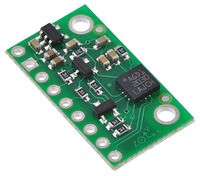
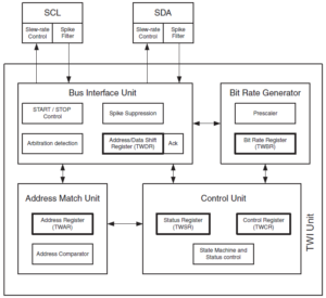
The I2C or TWI in Atmel speak, is a serial communications protocol with similar functionality to the SPI communications protocol. However, unlike the SPI which requires 4 pins to implement two-way communications, the I2C needs only two pins (SDA, SCL). The trade-off here is in the added complexity of the I2C interface. Today many intelligent sensors and actuators support both the I2C and SPI interface. This is the case with our L3G4200D 3-Axis Gyro Carrier with Voltage Regulator. As illustrated in Table 1.0 , the pins of the ATmega328P I2C subsystem are available for our sensors and actuators.
It should be noted that the I2C interface supports up to 128 devices without the need for any additional I/O pins.
Recovering I/O Resources
TBS
Rover Example
For our Rover we have the following Sensors and Actuators.
Sensors
I2C serial interface communicating with 3-Axis Gyroscope
I2C serial interface communicating with Current Sensor (optional)
I2C Arduino Nano (optional)
Analog input from Mid Range IR
Analog input from Long Range IR
Analog input from RC Circuit to 7.2V NiCD Battery – Dirty Power
Analog input from RC Circuit to 9V NiMH Battery – Clean Digital
Analog input from RC Circuit to 9V NiMH Battery – Camera
Four (4) Digital inputs from two (2) Shaft Encoders. Assumes full resolution of quadrature shaft encoders.
Actuators
Two (2) PWM outputs to H-Bridges controlling bipolar Stepper Motor – Adafruit Motorshield
Two (2) PWM outputs to H-Bridge controlling two DC Motors – Adafruit Motorshield
One PWM output to Servo – Adafruit Motorshield
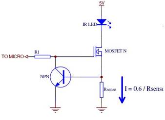
One Digital output thru a Transistor circuit to turn the Laser on/off
One Digital output thru a Transistor circuit to turn the Camera on/off
(One or more Digital outputs to address bits of a 4051 Analog MUX for camera battery)
For our example we begin by allocating resources interfaced to ATmega328P peripheral subsystems requiring the use of only one set of pins. In this case the I2C serial interface. Looking at the matrix we see that this first step removes two Analog inputs leaving us with four (4). We need five (5) Analog Inputs so we are already in trouble. We will leave the sensors and actuators wired to the GPIO peripheral subsystem to the end. This is because these are the simplest to assign.The PWM channels are output from the Adafruit Motor Shield and so easily assigned. Once again we have very few options with respect to which pins can be used. We are now left with 4 Digital Input and 2 Digital Output pins to be connected to the GPIO peripheral subsystem of the ATmega328P. So we need to find 6 (4 inputs + 2 outputs) GPIO pins. Looking at the matrix we see that we have 3 GPIO pins left. So we are three (3) I/O pins short. How we find the 1 analog and 3 GPIO pins is left up to you. Hint: Look-up 4051, 74HCT595, and parallel shift registers like the 74HC166, 74HC194, and CD4014.
Rover with Arduino Nano Example
In this design example to the chassis mounted Arduino Uno we add a Arduino Nano to the scan/tilt platform.
Scan / Tilt Platform
Sensors
Analog input from Mid Range IR
Analog input from Long Range IR
Analog input from RC Circuit to 9V NiMH Battery – Camera
Actuators
One PWM output to Servo – Adafruit Motorshield
One Digital output thru a Transistor circuit to turn the Laser on/off
One Digital output thru a Transistor circuit to turn the Camera on/off
Serial Communication
For our example we begin by allocating resources interfaced to ATmega328P peripheral subsystems requiring the use of only one set of pins. In this case the I2C serial interface. Looking at the matrix we see that this first step removes two Analog inputs leaving us with four (4). We need two (2) Analog Inputs so we have two (2) pins which may be used for sensors and actuators to be wired to the GPIO peripheral subsystem (PC 2 – 5). Four (4) of our six (6) PWM channels are required by the Adafruit Motor Shield. This leaves us with two (2) more pins which may be used for sensors and actuators to be wired to the GPIO peripheral subsystem. Looking at the matrix we see that we have 2 GPIO pins PD2 and PB5 which are unused, giving us a total of six (6) pins available to the GPIO peripheral subsystem. We only need four (4) for our two shaft encoders which means we have two (2) spare pins.
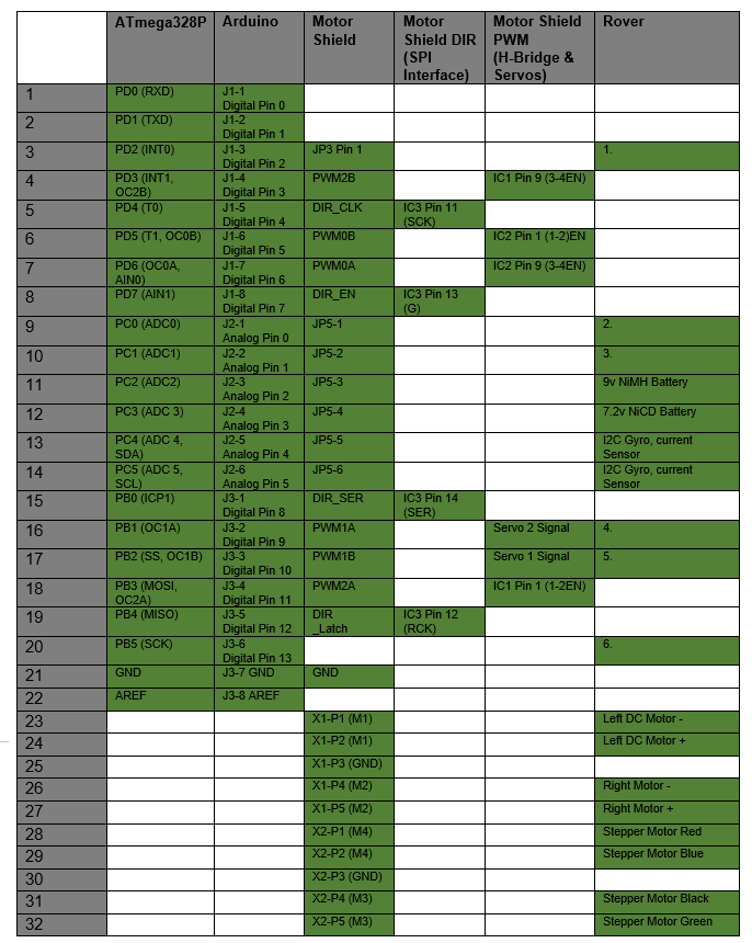 Table 3.0 System Resource Map for Chassis Mounted Arduino Uno
Software Programming in C++: Introduction
PDF Lecture http://web.csulb.edu/~hill/ee444/Lectures/02%20C++%20Introduction.pdf
READING
The AVR Microcontroller and Embedded Systems using Assembly and C
by Muhammad Ali Mazidi, Sarmad Naimi, and Sepehr Naimi
Sections: 7.1, 7.3, 7.4, 7.6
Here is a fun tool to translate your C++ code into Assembly
https://godbolt.org/
Table of Contents [hide]
Assemblers, Compilers, and Interpreters
Language Levels
- Scripting Arduino, Matlab
- High-Level JAVA, PYTHON
- Mid-Level C/C++
- Low-Level Assembly
From Humans to the Machine
Reference: https://en.wikipedia.org/wiki/Interpreted_language
Assembly 1:1
Machine Code
Compilers 1:X
Machine Code
Language examples = C/C++, Python, BASIC
Interpreters 1:1
bytecode
Language examples = C#, Java, Python, BASIC
Examples of Languages which may be Compiled or use an Interpreter
Most interpreted languages use an intermediate representation, which combines compiling and interpreting.
- JavaScript
- Python
- Ruby
VARIABLE PROPERTIES
- Data Type
- Scope
Scope
Scope allows the compiler to help us from making mistakes (overwriting the value of a variable) & allows us to help the compiler optimize the code (manage SRAM resources).
Reference: https://andrewharvey4.wordpress.com/tag/avr/
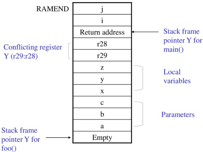
Supplemental figure for Volatile
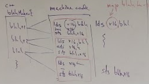
The key here may be the destruction of the mapping of variables to registers in the interrupted program.
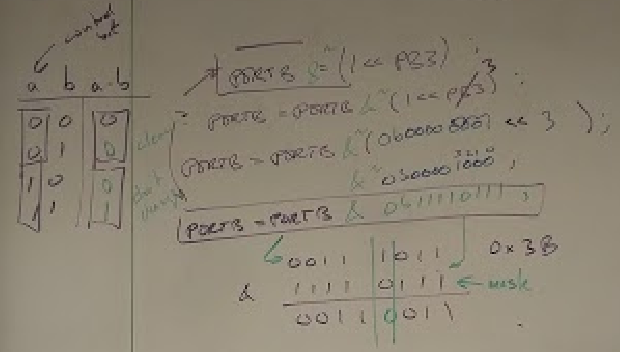
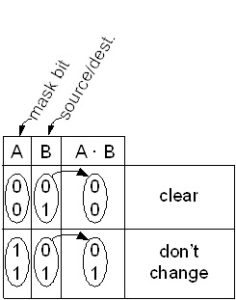
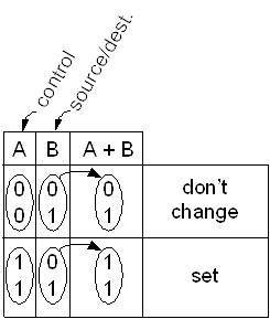
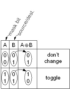
Supplemental figure for setting and clearing bits
Reference: http://web.csulb.edu/~hill/ee346/Lectures/14%20AVR%20Logic%20and%20Shift.pdf
Data Types
Explicit Data Types
source: Wikipedia stdint.h
- The C standard library introduced in the C99 standard library (stdint.h) allows programmers to write more portable code by allowing them to specify exact-width integer types, together with the defined minimum and maximum allowable values for each type.
- This new library is particularly useful for embedded programming which often involves considerable manipulation of hardware specific I/O registers requiring integer data of fixed widths, specific locations and exact alignments.
- The naming convention for exact-width integer types is intN_t for signed integers and uintN_t for unsigned integers. For example
uint16_t revsteps; // # steps per revolution
uint8_t steppernum;
uint32_t usperstep, steppingcounter;
Implicit and Architecture Dependent Data Types
| Data Type | Size in Bits | Data Range / Usage |
|---|---|---|
| void | ||
| boolean | ||
| char | 8 | -128 to +127 |
| unsigned char | 8 | 0 to 255 |
| byte | 8 | 0 to 255 |
| int | 16 | -32,768 to +32,767 |
| unsigned int | 16 | 0 to 65,535 |
| word | 16 | 0 to 65,535 (Arduino) |
| long | 32 | -2,147,483,648 to +2,147,483,648 |
| unsigned long | ||
| float | 32 | +/-1.175e-38 to +/-3.402e38 |
| double | 32 | +/-1.175e-38 to +/-3.402e38 |
| string – char array | ||
| String – object | ||
| array |
Utilities
sizeof()
The sizeof operator returns the number of bytes in a variable type, or the number of bytes occupied by an array.
VARIABLE SCOPE
Variable Scope
- Variables in the C programming language, which Arduino uses, have a property called scope.
- A Global variable is one that you can access anywhere in a program. Local variables are only visible to the function in which they are declared. In the Arduino environment, any variable declared outside of a function.
- Local variables insure that only one function has access to its own variables. This prevents programs from inadvertently modifying variables used by another function.
- A variable declared inside brackets {} can only be accessed within said brackets.
Source: Arduino – Variable Scope
uint gPWMval; // any function will see this variable
void setup()
{
// …
}
void loop()
{
int i; // “i” is only “visible” inside of “loop”
float f; // “f” is only “visible” inside of “loop”
// …
for (int j = 0; j <100; j++){
// variable j can only be accessed inside the
// for-loop brackets
}
}
QUALIFIERS
Static
- The static keyword is used to create variables that are visible to only one function. However unlike local variables that get created and destroyed every time a function is called, static variables persist beyond the function call, preserving their data between function calls.
- Variables declared as static will only be created and initialized the first time a function is called.
source: COMP2121: Microprocessors and Interfacing
http://www.cse.unsw.edu.au/~cs2121
int randomWalk(int moveSize){
static int place; // variable to store value in random walk,
// declared static so that it stores
// values in between function calls, but
// no other functions can change its value
place = place + (random(-moveSize, moveSize + 1));
// check lower and upper limits
if (place < randomWalkLowRange){ place = randomWalkLowRange; } else if(place > randomWalkHighRange){
place = randomWalkHighRange;
}
return place;
}
Volatile
- The volatile qualifier directs the compiler to load the variable from RAM and not from a general purpose register (R0 – R31),
- A variable should be declared volatile when used within an Interrupt Service Routine (ISR).
- For more on Interrupts visit Gammon Software Solutions forum
// toggles LED when interrupt pin changes state
int pin = 13;
volatile int state = LOW;
void setup()
{
pinMode(pin, OUTPUT);
attachInterrupt(0, blink, CHANGE);
}
void loop()
{
digitalWrite(pin, state);
}
void blink()
{
state = !state;
}
Const
Reference: The C++ ‘const’ Declaration: Why & How
- The const qualifier declares a variable as a constant.
Example
// create integer constant myConst with value 33
const int myConst=33;
- Such constants are useful for parameters which are used in the program but do not need to be changed after the program is compiled.
- It has an advantage over the C preprocessor ‘#define’ command in that is understood and used by the compiler itself.
- Use of constant checked for scope.
- Use of constant checked for datatype.
- As a result error messages are much more helpful.
- Example usage is in the definition of a base pointer to an array
Example
// The compiler will replace any mention of
// ledPin with the value 3 at compile time.
#define ledPin 3
- Constants are saved in SRAM not in Flash Program Memory (C was originally designed for Princeton based Machines). Click here to learn how to save data to Flash Program Memory.
Arduino Scripting Language
Reference
Arduino Language Reference
Arduino programs can be divided in three main parts: structure, values (variables and constants), and functions.
Structure
Control Structures
Further Syntax
- ; (semicolon)
- {} (curly braces)
- // (single line comment)
- /* */ (multi-line comment)
- #define
- #include
Arithmetic Operators
Comparison Operators
- == (equal to)
- != (not equal to)
- < (less than)
- > (greater than)
- <= (less than or equal to)
- >= (greater than or equal to)
Boolean Operators
Pointer Access Operators
Bitwise Operators
- & (bitwise and)
- | (bitwise or)
- ^ (bitwise xor)
- ~ (bitwise not)
- << (bitshift left)
- >> (bitshift right)
Compound Operators
- ++ (increment)
- — (decrement)
- += (compound addition)
- -= (compound subtraction)
- *= (compound multiplication)
- /= (compound division)
- &= (compound bitwise and)
- |= (compound bitwise or)
When we start constructing compound assignment statements in order to assign values to fields within a peripheral subsystem register, also known as a special function register (SFR), it is important to remember operator precedence.
| Level | Operator | Description | Grouping |
| 1 | :: | scope | Left-to-right |
| 2 | () [] . -> ++ — dynamic_cast static_cast reinterpret_cast const_cast typeid | postfix | Left-to-right |
| 3 | ++ — ~ ! sizeof new delete | unary (prefix) | Right-to-left |
| * & | indirection and reference (pointers) | ||
| + – | unary sign operator | ||
| 4 | (type) | type casting | Right-to-left |
| 5 | .* ->* | pointer-to-member | Left-to-right |
| 6 | * / % | multiplicative | Left-to-right |
| 7 | + – | additive | Left-to-right |
| 8 | << >> | shift | Left-to-right |
| 9 | < > <= >= | relational | Left-to-right |
| 10 | == != | equality | Left-to-right |
| 11 | & | bitwise AND | Left-to-right |
| 12 | ^ | bitwise XOR | Left-to-right |
| 13 | | | bitwise OR | Left-to-right |
| 14 | && | logical AND | Left-to-right |
| 15 | || | logical OR | Left-to-right |
| 16 | ?: | conditional | Right-to-left |
| 17 | = *= /= %= += -= >>= <<= &= ^= |= | assignment | Right-to-left |
| 18 | , | comma | Left-to-right |
Values
Constants
Data Types (see above)
Functions – Scripting Language
Digital I/O
- pinMode() // Writes to GPIO DDR register
- digitalWrite() // Writes to GPIO Port register
- digitalRead() // Reads GPIO Pin register
Analog I/O
- analogReference() // Writes to bits REFS1:REFS0 of ADMUX register
- analogRead() // Reads ADC Data register (ADCH/ADCL)
- analogWrite() // Writes to OCRnA or OCRnB registers of Timers
Advanced I/O
- tone()
- noTone()
- shiftOut() // Software implementation of SPI MOSI interface
- shiftIn() // Software implementation of SPI MISO interface
- pulseIn()
Time
- millis()
- micros()
- delay()
- delayMicroseconds()
Math
Trigonometry
Random Numbers
- randomSeed()
- random()
Bits and Bytes
External Interrupts
- attachInterrupt() // Configures external interrupt pins INT1 and INT0
- detachInterrupt() // Clears EIMSK register bits INT1 and INT0
Interrupts
- interrupts() // Sets SREG I bit
- noInterrupts() // Clears SREG I bit
Communication
WORKING WITH BITS IN C++
Resources
1. Arduino
2. AVR-libc
Set/Clear a Bit
Assembly
GPIO Port (first 32 I/O addresses)
| sbi PORTB, PB3 | cbi PORTB, PB3 |
IO Address Space
| in r16, PORTB sbr r16, 0b00001000 out PORTB, r16 |
in r16, PORTB cbr r16, 0b00001000 out PORTB, r16 |
| // Set a Bit | // Clear a Bit |
| digitalWrite(MOTORLATCH, HIGH); | digitalWrite(MOTORLATCH, LOW); |
| // Set a Bit | // Clear a Bit |
| PORTB |= _BV(PB3); or sbi(PORTB, PB3); // deprecated |
PORTB &= ~_BV(PB3); or cbi(PORTB, PB3); // deprecated |
The AVR C library includes the following definition
#include
// _BV Converts a bit number into a Byte Value (BV).
#define _BV(bit) (1 << (bit)) // : Special function registers
C/C++
| // Set a Bit | // Clear a Bit |
| PORTB |= (1 << (PB3)); | PORTB &= ~(1 << (PB3)); |
Set a Bit Pattern
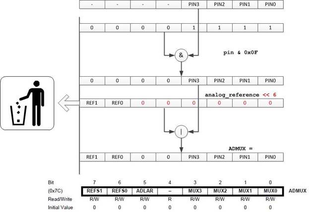
ADC Subsystem ADMUX Register Example
In this example we set/clear 2 fields within a byte. Undefined bits are cleared.
ADMUX = (analog_reference << 6) | (pin & 0x0f); // analogRead
Test Your Knowledge 1: Assume a function of type uint16_t. What would be returned if high = A and low = 3?
return (high << 8) | low;
0x0A03
Test Your Knowledge 2: How could you modify the ADMUX example to allow the programmer to set or clear the ADC Left Adjust Result ADLAR bit? Answer
ADMUX = (analog_reference << 6) | (pin & 0x0f) | ((left_adjust & 0x01) << 5);
note: if left_adjust is zero ADLAR bit stays at zero.
Program Example:
Here is my Arduino Test Script ported to AVR Studio so I could use the simulator: ArduinoToAVRStudio-Blink ****
In our first example “ADC Subsystem ADMUX Register” we assumed where each field was located within the register. In the next example we do not presuppose the location of the fields. This allows our program to adapt to different microcontroller register definitions. The downside is that, while in the first example the fields could be defined on the fly by the user (for example as arguments to a function), in this next example they must be predefined.
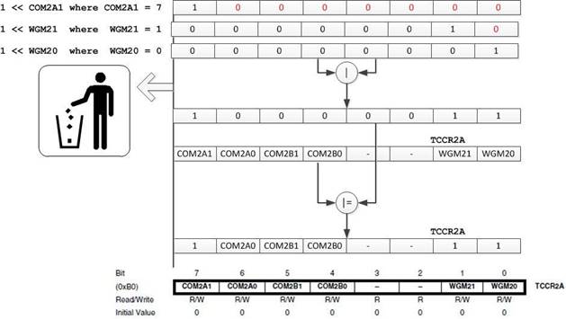
Timer/Counter 2 Control Register A Example 1
In this example, the wave generation mode of Timer/Counter 2 (WGM21:WGM20) is set to Fast PWM (0b11), the compare match output A mode (COM2A1:COM2A0) is configured to set on compare match (0b10), while the configuration bits for output compare register B are not modified (COM2B1:COM2B0).
#define _BV(bit) (1 << (bit))
TCCR2A |= _BV(COM2A1)|_BV(WGM21)|_BV(WGM20); // fast PWM, turn on oc0
Test Your Knowledge 3: At reset TCCR2A is cleared so our C++ example would result in COM2A1:COM2A0 = 0b10. What if another piece of software had set COM2A0 to 1 before this initialization routine was called. In this case our C++ code would not configure the register as expected. How could you solve this problem? Tip: Because of operator precedence (see Compound Operators earlier in this document) you will need to use a simple assignment operator or write two lines of code.
AnswerTCCR2A &= ~_BV(COM2A0)
Timer/Counter 2 Control Register A Example 2
In this example, the wave generation mode of Timer/Counter 2 (WGM21:WGM20) is set to Phase Correct PWM (0b01). The compare match output A mode (COM2A1:COM2A0) is configured to set on compare match, while the configuration bits for output compare register B are not modified (COM2B1:COM2B0). This example makes no assumption about the state of the bits within the WGM or COM2A bit fields.
TCCR2A &= ~_BV(COM2A0) & ~_BV(WGM21); // clear bits
TCCR2A |= _BV(COM2A1) | _BV(WGM20); // set bits
Test Your Knowledge 4: Can you combine these two expressions into one?
AnswerTCCR2A = TCCR2A&~(_BV(WGM21) | _BV(COM2A0)) | _BV(WGM20) | _BV(COM2A1);
Test Your Knowledge 5: If you are allowed to assume the location of the waveform generation mode (WGM2) and the compare match output A mode (COM2A) fields within the TCCR2A register, how would you write an expression that could set these two fields based on user defined variables output_mode and waveform? Hint: see the first example.
AnswerTCCR2A |= (output_mode << 6) | (waveform & 0x03); // analogRead
Test if a Bit is Set or Cleared
source: Special function registers
| #define | bit_is_set(sfr, bit) (_SFR_BYTE(sfr) & _BV(bit)) |
| #define | bit_is_clear(sfr, bit) (!(_SFR_BYTE(sfr) & _BV(bit))) |
| #define | loop_until_bit_is_set(sfr, bit) do { } while (bit_is_clear(sfr, bit)) |
| #define | loop_until_bit_is_clear(sfr, bit) do { } while (bit_is_set(sfr, bit)) |
ADC Subsystem ADMUX Register Example
// ADSC is cleared when the conversion finishes
while (bit_is_set(ADCSRA, ADSC));
What is _SFR_BYTE(sfr)?
Source: Playing with Arduino _SFR_BYTE() and PORT
The _SFR_BYTE() is a macro that returns a byte of data of the specified address. The _SFR_BYTE() is defined in hardware/tools/avr/avr/include/avr/sfr_defs.h as below.
#define _SFR_BYTE(sfr) _MMIO_BYTE(_SFR_ADDR(sfr))
The _SFR_ADDR() is a macro that expands the _SFR_MEM_ADDR(sfr) macro. Both are defined in hardware/tools/avr/avr/include/avr/sfr_defs.h as below.
#define _SFR_ADDR(sfr) _SFR_MEM_ADDR(sfr)
The _SFR_MEM_ADDR() is a macro that returns the address of the argument.
#define _SFR_MEM_ADDR(sfr) ((uint16_t) &(sfr))
The _MMIO_BYTE() is a macro that dereferences a byte of data at the specified address. The _MMIO_BYTE() is defined in hardware/tools/avr/avr/include/avr/sfr_defs.h as below. The input is mem_addr and dereferences its contents.
#define _MMIO_BYTE(mem_addr) (*(volatile uint8_t *)(mem_addr))
Putting it all together, this is how the compiler would expand _SFR_BYTE(sfr)
_SFR_BYTE(sfr) *(volatile uint8_t * uint16_t &(sfr))
Let’s take a closer look at this expanded macro definition. Starting from the inside and moving out. The ampersand sign (&) is known as a reference operator and lets the compiler know that “sfr” is to be interpreted as an address (i.e., a pointer). Specifically, a 16-bit address (uint16_t).
The asterisk (*) sign in the uint8_t declaration of the pointer does not mean “value pointed by”, it only means that it is a pointer (it is part of its type compound specifier). It should not be confused with the dereference operator, which come next, they are simply two different things represented with the same sign.
The final asterisk sign (*) at the beginning of the statement is a dereference operator. When the dereference operator is used you will get the “value pointed by” a pointer – the actual value of the register.
Mapping the 6-bit I/O address space into the 16-bit extended I/O address space
This works if the “special function register” is in the extended I/O address space but what if it is in the 64 byte I/O address space?
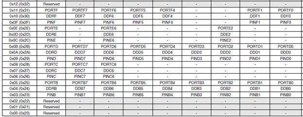
Let’s assume sfr is within the I/O address space of the ATmega microcontroller, for example a GPIO Port. Each GPIO Port includes three registers PINx, DDRx, and PORTx. For the ATmega32U4 “x” would be B, C, D, E, and F
To continue our example let’s assume we are going to write to one of the PORT registers (not to be confused with the PORT itself – see figure above). The PORTB, PORTC and PORTD registers are defined in hardware/tools/avr/avr/include/avr/iom32u4.h as below.
#define PORTB _SFR_IO8(0x05)
#define PORTC _SFR_IO8(0x08)
#define PORTD _SFR_IO8(0x0B)
Again looking at the figure, we see that arguments 0x05, 0x07, and 0x0A are the I/O addresses of PORTB, PORTC and PORTD respectively. They call _SFR_IO8(). The _SFR_IO8() converts the I/O address to the memory address. It is a macro that returns a byte of data at an address of io_addr + __SFR_OFFSET. The _SFR_IO8() is defined in hardware/tools/avr/avr/include/avr/sfr_defs.h as below.
#define _SFR_IO8(io_addr) _MMIO_BYTE((io_addr) + __SFR_OFFSET)
#define __SFR_OFFSET 0x20
Again, _MMIO_BYTE() is a macro that dereferences a byte of data at the specified address.
#define _MMIO_BYTE(mem_addr) (*(volatile uint8_t *)(mem_addr))
Putting it all together we have the equivalent macro.
#define _SFR_IO8(io_addr) (*(volatile uint8_t *)(mem_addr)) + 0x20
Appendix
Appendix A: The Arduino Family Tree
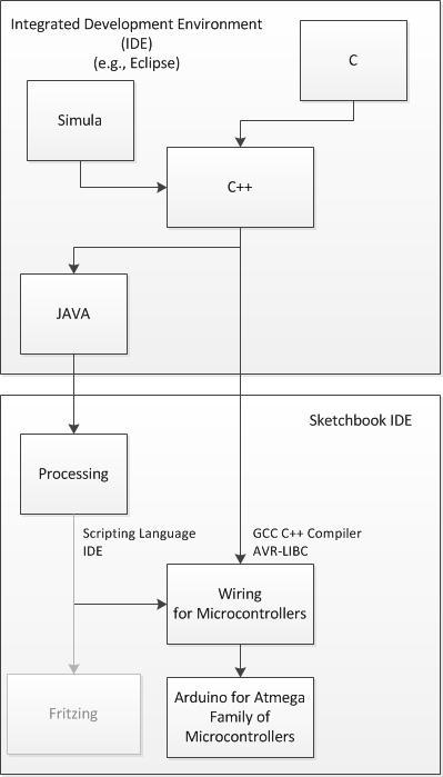
The Arduino language (based on Wiring) is implemented in C/C++, and therefore has some differences from the Processing language, which is based on Java.
A Visual Paradigm for Programming – Processing
Source: Wikipedia – Processing (programming language)
- Processing was designed to get non-programmers (originally electronic artists) started with software programming, using a visual context, and to serve as the foundation for electronic sketchbooks.
- The concept of “visual context” makes Processing comparable to Adobe’s ActionScript and Lingo scripting based languages.
- A “sketchbook”, is a minimal alternative to an integrated development environment (IDE)
- Processing is an open source programming language and integrated development environment (IDE)
- The project was initiated in 2001 by Casey Reas and Benjamin Fry, both formerly of the Aesthetics and Computation Group at the MIT Media Lab.
- The language builds on the Java programming language, but uses a simplified syntax and graphics programming model.
From Programming to Microcontrollers – Wiring
- Wiring was design to teach non-programmers (originally electronic artists) how to program microcontrollers.
- Wiring, uses the Processing IDE (sketchbook) together with a simplified version of the C++ programming language (gcc compiler)
- There are now two separate hardware projects, Wiring and Arduino, using the Wiring IDE (sketchbook) and language.
- Fritzing is another software environment of the same sort, which helps designers and artists to document their interactive prototypes and to take the step from physical prototyping to actual product.
From Programming Microcontrollers to the Arduino
Arduino is an open-source electronics prototyping platform based on flexible, easy-to-use hardware and software. It’s intended for artists, designers, hobbyists, and anyone interested in creating interactive objects or environments.
- The C/C++ language is the foundation upon which the Arduino language (like Wiring on which it is based) is built.
- The C/C++ language is implemented using the GCC Compiler and links against the AVR C library AVR Libc and allows the use of any of its functions; see its user manual for details.
- The AVR C Library has its own family tree (nongnu, gcc)
APPENDIX B: Standard Libraries
- EEPROM – reading and writing to “permanent” storage (EEPROM)
- Ethernet – for connecting to the internet using the Arduino Ethernet Shield
- Firmata – for communicating with applications on the computer using a standard serial protocol.
- LiquidCrystal – for controlling liquid crystal displays (LCDs)
- SD – for reading and writing SD cards
- Servo – for controlling servo motors
- SPI – for communicating with devices using the Serial Peripheral Interface (SPI) Bus
- SoftwareSerial – for serial communication on any digital pins
- Stepper – for controlling stepper motors
- Wire – Two Wire Interface (TWI/I2C) for sending and receiving data over a net of devices or sensors.
APPENDIX C: C++ OPERATOR PRECEDENCE
When we start constructing compound assignment statements in order to assign values to fields within a peripheral subsystem register, also known as a special function register (SFR), it is important to remember operator precedence.
| Level | Operator | Description | Grouping |
| 1 | :: | scope | Left-to-right |
| 2 | () [] . -> ++ — dynamic_cast static_cast reinterpret_cast const_cast typeid | postfix | Left-to-right |
| 3 | ++ — ~ ! sizeof new delete | unary (prefix) | Right-to-left |
| * & | indirection and reference (pointers) | ||
| + – | unary sign operator | ||
| 4 | (type) | type casting | Right-to-left |
| 5 | .* ->* | pointer-to-member | Left-to-right |
| 6 | * / % | multiplicative | Left-to-right |
| 7 | + – | additive | Left-to-right |
| 8 | << >> | shift | Left-to-right |
| 9 | < > <= >= | relational | Left-to-right |
| 10 | == != | equality | Left-to-right |
| 11 | & | bitwise AND | Left-to-right |
| 12 | ^ | bitwise XOR | Left-to-right |
| 13 | | | bitwise OR | Left-to-right |
| 14 | && | logical AND | Left-to-right |
| 15 | || | logical OR | Left-to-right |
| 16 | ?: | conditional | Right-to-left |
| 17 | = *= /= %= += -= >>= <<= &= ^= |= | assignment | Right-to-left |
| 18 | , | comma | Left-to-right |
APPENDIX D: ARDUINO ANALOGREAD FUNCTION
int analogRead(uint8_t pin)
{
uint8_t low, high;
// set the analog reference (high two bits of ADMUX) and select the
// channel (low 4 bits). this also sets ADLAR (left-adjust result)
// to 0 (the default).
ADMUX = (analog_reference << 6) | (pin & 0x0f);
// without a delay, we seem to read from the wrong channel
//delay(1);
// start the conversion
sbi(ADCSRA, ADSC);
// ADSC is cleared when the conversion finishes
while (bit_is_set(ADCSRA, ADSC));
// we hto read ADCL first; doing so locks both ADCL
// and ADave CH until ADCH is read. reading ADCL second would
// cause the results of each conversion to be discarded,
// as ADCL and ADCH would be locked when it completed.
low = ADCL;
high = ADCH;
// combine the two bytes
return (high << 8) | low;
}
APPENDIX E: ADAFRUIT MOTOR SHIELD
Using the Motor Shield
DC Motors
#include
// motor is an instance of the AF_DCMotor class
AF_DCMotor motor(2, MOTOR12_64KHZ); // create motor #2, 64KHz pwm
void setup() {
Serial.begin(9600); // set up Serial library at 9600 bps
Serial.println(“Motor test!”);
motor.setSpeed(200); // set the speed to 200/255
}
void loop() {
Serial.print(“tick”);
motor.run(FORWARD); // turn it on going forward
delay(1000);
Serial.print(“tock”);
motor.run(BACKWARD); // the other way
delay(1000);
Serial.print(“tack”);
motor.run(RELEASE); // stopped
delay(1000);
}
Stepper Motor
#include
// motor is an instance of the AF_Stepper class
AF_Stepper motor(48, 2);
void setup() {
Serial.begin(9600); // set up Serial library at 9600 bps
Serial.println(“Stepper test!”);
motor.setSpeed(10); // 10 rpm
motor.step(100, FORWARD, SINGLE);
motor.release();
delay(1000);
}
void loop() {
motor.step(100, FORWARD, SINGLE);
motor.step(100, BACKWARD, SINGLE);
motor.step(100, FORWARD, DOUBLE);
motor.step(100, BACKWARD, DOUBLE);
motor.step(100, FORWARD, INTERLEAVE);
motor.step(100, BACKWARD, INTERLEAVE);
motor.step(100, FORWARD, MICROSTEP);
motor.step(100, BACKWARD, MICROSTEP);
}
Library Header
What is a Library?
// Adafruit Motor shield library
// copyright Adafruit Industries LLC, 2009
// this code is public domain, enjoy!
#ifndef _AFMotor_h_
#define _AFMotor_h_
#include
#include
//#define MOTORDEBUG 1
#define MICROSTEPS 16 // 8 or 16
#define MOTOR12_64KHZ _BV(CS20) // no prescale
#define MOTOR12_8KHZ _BV(CS21) // divide by 8
#define MOTOR12_2KHZ _BV(CS21) | _BV(CS20) // divide by 32
#define MOTOR12_1KHZ _BV(CS22) // divide by 64
#define MOTOR34_64KHZ _BV(CS00) // no prescale
#define MOTOR34_8KHZ _BV(CS01) // divide by 8
#define MOTOR34_1KHZ _BV(CS01) | _BV(CS00) // divide by 64
#define MOTOR1_A 2
#define MOTOR1_B 3
#define MOTOR2_A 1
#define MOTOR2_B 4
#define MOTOR4_A 0
#define MOTOR4_B 6
#define MOTOR3_A 5
#define MOTOR3_B 7
#define FORWARD 1
#define BACKWARD 2
#define BRAKE 3
#define RELEASE 4
#define SINGLE 1
#define DOUBLE 2
#define INTERLEAVE 3
#define MICROSTEP 4
// Arduino pin names
#define MOTORLATCH 12
#define MOTORCLK 4
#define MOTORENABLE 7
#define MOTORDATA 8
class AFMotorController
{
public:
AFMotorController(void);
void enable(void);
friend class AF_DCMotor;
void latch_tx(void);
};
class AF_DCMotor
{
public:
AF_DCMotor(uint8_t motornum, uint8_t freq = MOTOR34_8KHZ);
void run(uint8_t);
void setSpeed(uint8_t);
private:
uint8_t motornum, pwmfreq;
};
class AF_Stepper {
public:
AF_Stepper(uint16_t, uint8_t);
void step(uint16_t steps, uint8_t dir, uint8_t style = SINGLE);
void setSpeed(uint16_t);
uint8_t onestep(uint8_t dir, uint8_t style);
void release(void);
uint16_t revsteps; // # steps per revolution
uint8_t steppernum;
uint32_t usperstep, steppingcounter;
private:
uint8_t currentstep;
};
uint8_t getlatchstate(void);
#endif
Adafruit Private Functions
latch_tx
#define _BV(bit) (1 << (bit))
/*
Send data located in 8-bit variable latch_state
to the 74HC595 on the Motor Shield.
*/
void AFMotorController::latch_tx(void) {
uint8_t i;
//LATCH_PORT &= ~_BV(LATCH);
digitalWrite(MOTORLATCH, LOW); // – Output register clock low
//SER_PORT &= ~_BV(SER);
digitalWrite(MOTORDATA, LOW); // – Serial data bit = 0
for (i=0; i<8; i++) { // – Shift out 8-bits
//CLK_PORT &= ~_BV(CLK);
digitalWrite(MOTORCLK, LOW); // – Shift clock low
if (latch_state & _BV(7-i)) { // – Is current bit of
//SER_PORT |= _BV(SER); latch_state == 1
digitalWrite(MOTORDATA, HIGH); // – Yes, serial data bit = 1
} else {
//SER_PORT &= ~_BV(SER);
digitalWrite(MOTORDATA, LOW); // – No, serial data bit = 0
}
//CLK_PORT |= _BV(CLK);
digitalWrite(MOTORCLK, HIGH); // – Shift clock high, rising edge
} // shift bit into shift register
//LATCH_PORT |= _BV(LATCH);
digitalWrite(MOTORLATCH, HIGH); // – Output register clock high, rising
} // edge sends the stored bits to the
// output register.
enable
/*
Configure DDR Registers B and D bits assigned to
the input of the 74HC595 on the Motor Shield. Output
all zeros and enable outputs.
*/
void AFMotorController::enable(void) {
// setup the latch
/*
LATCH_DDR |= _BV(LATCH);
ENABLE_DDR |= _BV(ENABLE);
CLK_DDR |= _BV(CLK);
SER_DDR |= _BV(SER);
*/
pinMode(MOTORLATCH, OUTPUT);
pinMode(MOTORENABLE, OUTPUT);
pinMode(MOTORDATA, OUTPUT);
pinMode(MOTORCLK, OUTPUT);
latch_state = 0;
latch_tx(); // “reset”
//ENABLE_PORT &= ~_BV(ENABLE); // enable the chip outputs!
digitalWrite(MOTORENABLE, LOW);
}
Adafruit Motor Public Functions
run
void AF_DCMotor::run(uint8_t cmd) {
uint8_t a, b;
/* Section 1: choose two shift register outputs based on which
* motor this instance is associated with. motornum is the
* motor number that was passed to this instance’s constructor.
*/
switch (motornum) {
case 1:
a = MOTOR1_A; b = MOTOR1_B; break;
case 2:
a = MOTOR2_A; b = MOTOR2_B; break;
case 3:
a = MOTOR3_A; b = MOTOR3_B; break;
case 4:
a = MOTOR4_A; b = MOTOR4_B; break;
default:
return;
}
/* Section 2: set the selected shift register outputs to high/low,
* low/high, or low/low depending on the command. This is done
* by updating the appropriate bits of latch_state and then
* calling tx_latch() to send latch_state to the chip.
*/
switch (cmd) {
case FORWARD: // high/low
latch_state |= _BV(a);
latch_state &= ~_BV(b);
MC.latch_tx();
break;
case BACKWARD: // low/high
latch_state &= ~_BV(a);
latch_state |= _BV(b);
MC.latch_tx();
break;
case RELEASE: // low/low
latch_state &= ~_BV(a);
latch_state &= ~_BV(b);
MC.latch_tx();
break;
}
}
setSpeed
void AF_DCMotor::setSpeed(uint8_t speed) {
switch (motornum) {
case 1:
OCR2A = speed; break;
case 2:
OCR2B = speed; break;
case 3:
OCR0A = speed; break;
case 4:
OCR0B = speed; break;
}
}
initPWM1
This is a brief excerpt of the AF_DCMotor constructor (subroutine initPWM1(freq)), which is initializing speed control for motor 1:
// use PWM from timer2A
TCCR2A |= _BV(COM2A1) | _BV(WGM20) | _BV(WGM21); // fast PWM, turn on oc0
TCCR2B = freq & 0x7;
OCR2A = 0;
DDRB |= _BV(3);
break;
General Purpose I/O Ports
Table of Contents [hide]
Source: ATmega328P Data Sheet http://www.atmel.com/dyn/resources/prod_documents/8161S.pdf page 5
ATMEGA GENERAL PURPOSE DIGITAL I/O PORTS
Reading: Section 6.1.1 Introduction
- The ATmega32U4 has 26 General Purpose Digital I/O Pins assigned to 5 Ports (8-bit Ports B, D, 2-bit Port C,E, and 6-bit Port F)
- Each I/O port pin may be configured as an output with symmetrical drive characteristics. Each pin driver is strong enough (20 mA) to drive LED displays directly.
- Each I/O port pin may be configured as an input with or without a pull-up resistor. The values for the pull up resistor can range from 20 – 50 K ohms.
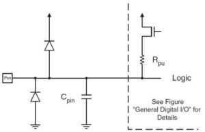
- Each I/O pin has protection diodes to both VCC and Ground
PIN DESCRIPTION OF THE ATMEGA32U4
Reading: Section 6.1.3 Pin-Muxing
I/O Ports B, C, D, E, and F
Ports B (PB7..PB0), C (PC7,PC6), D (PD7..PD0), E (PE6,PE2), F (PF7..PF4,PF1,PF0) are bi-directional I/O ports with internal pull-up resistors (selected for each bit). The Port output buffers have symmetrical drive characteristics with both high sink and source capability.
Interrupts
External Interrupts are triggered by the INT0 to INT3 and INT6 pins or any of the PCINT7..0 pins associated with Port B. Observe that, if enabled, the interrupts will trigger even if the pins are configured as outputs. This feature provides a way of generating a software interrupt.
Analog Voltage (AVCC)
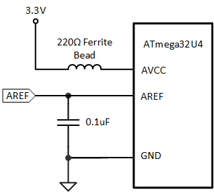
AVCC is the supply voltage pin for the A/D Converter. It should be externally connected to VCC. If the ADC is used, it should be connected to VCC through a low-pass filter.
Analog Reference (AREF)
AREF is the analog reference pin for the A/D Converter.
Analog to Digital Converter (ADC)
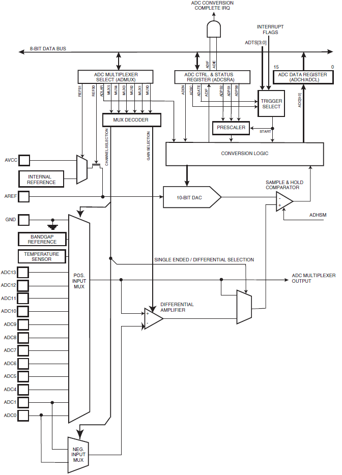
The ATmega32U4 includes a 10-bit ADC. The ADC is connected to a analog multiplexer with six single-ended voltage input (ADC0, ADC1, ADC4 to ADC7) channels. The device also supports differential inputs, with the positive input terminal selectable between ADC4 to ADC7, and negative input terminal selectable between ADC0 and ADC1. The output of the differential amplifier goes to a gain stage, with four (4) programmable amplification steps of 0 dB (1x), 10 dB (10x), 16dB (40x), and 23dB (200x). If 1x, 10x, or 40x gain is used, 8-bit resolution can be expected. If 200x gain is used, 7-bit resolution can be expected.
I/O PORT PIN AS AN OUTPUT
Reading: Section 6.1.2 Basic Operation
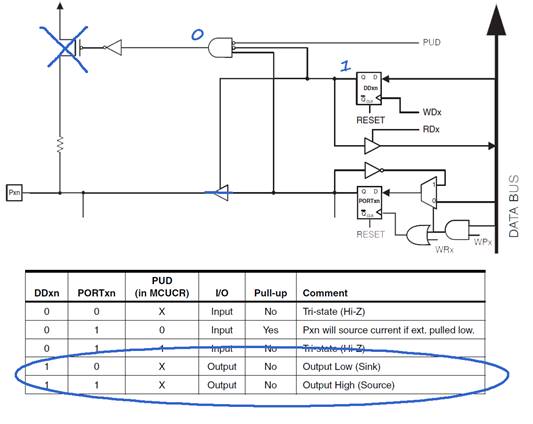
- To configure a Port (x) pin as an output set corresponding bit (n) in the Data Direction Register (DDxn) to 1. Once configured as an output pin, you control the state of the pin (1 or 0) by writing to the corresponding bit (n) of the PORTxn
- Writing (signal WPx) a logic one to PINxn toggles the value of PORTxn, independent on the value of DDxn. Note that the SBI instruction can be used to toggle one single bit in a port.
I/O PORT PIN AS AN INPUT
Reading: Section 6.2 Input
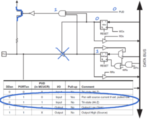
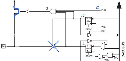
- To configure a Port (x) pin as an input set corresponding bit (n) in the Data Direction Register (DDxn) to 0. To add a pull-up resistor set the corresponding bit (n) of the PORTxn register to 1 (see illustration).
- You can now read the state of the input pin by reading the corresponding bit (n) of the PINxn
ACCESSING GPIO LINES IN ASSEMBLY and C++
DESIGN EXAMPLE 1 – Initialize 3DoT
Problem: When power is applied to the ATmega32U4 on the 3DoT board, it needs to be configured. However, because the 3DoT board, like the Arduino UNO, is itself integrated into another system, it is not completely aware of its environment. Therefore, pins allocated to the shields should not be modified.
The following tables show how the code should configure Ports B (PB7..PB0), C (PC7,PC6), D (PD7..PD0), E (PE6,PE2), F (PF7..PF4,PF1,PF0).
Port B
| PIN | PB7 | PB6 | PB5 | PB4 | PB3 | PB2 | PB1 | PB0 |
| J5-1 | J5-2 | J5-3 | J5-4 | |||||
| NET | AIN1 | BIN2 | NC | NC | MISO | MOSI | SCK | SS |
| DDRB | 1 | 1 | 0 | 0 | X | X | X | X |
| PORTB | 0 | 0 | 1 | 1 | X | X | X | X |
/* undefind pins are not changed */
/* pins that are not connected are defined as inputs with pull-up resistors */
DDRB  &= 0x0F;   // clear most significant nibble
DDRB  |= 0xC0;   // set bit pattern
PORTB &= 0x0F;   // clear most significant nibble
PORTB |= 0x30;   // set bit pattern
Port C
| PIN | PC7 | PC6 | PC5 | PC4 | PC3 | PC2 | PC1 | PC0 |
| NET | BIN1 | NC | – | – | – | – | – | – |
| DDRC | 1 | 0 | – | – | – | – | – | – |
| PORTC | 0 | 1 | – | – | – | – | – | – |
DDRC  &= 03F;  // clear most significant 2 bits
DDRC  |= 0x80; // set bit pattern
PORTC &= 03F;  // clear most significant 2 bits
PORTC |= 0x40;
Port D
| PIN | PD7 | PD6 | PD5 | PD4 | PD3 | PD2 | PD1 | PD0 |
| Servo A | LED | Servo B | J1-5 | J1-4 | J3-3 | J3-2 | ||
| NET | AIN2 | SIG | BUILTIN | SIG | TX | RX | SDA | SCL |
| DDRD | 1 | 1 | 1 | 1 | X | X | X | X |
| PORTD | 0 | 0 | 0 | 0 | X | X | X | X |
DDRD  |= 0xF0; // set most significant nibble
PORTD &= 0x0F; // clear most significant nibble
Port E
| PIN | PE7 | PE6 | PE5 | PE4 | PE3 | PE2 | PE1 | PE0 |
| S-1 | ||||||||
| NET | – | NC | – | – | – | SW | – | – |
| DDRE | – | 0 | – | – | – | 0 | – | – |
| PORTE | – | 1 | – | – | – | 0 | – | – |
DDRE  &= 0xBB;  // clear bits 6 and 2
PORTE &= 0xBB;  // clear bits 6 and 2
PORTE |= 0x40;  // set bit pattern
Port F
| PIN | PF7 | PF6 | PF5 | PF4 | PF3 | PF2 | PF1 | PF0 |
| J2-5 | J2-6 | J2-7 | J2-8 | J2-6 | ||||
| NET | A0 | A1 | A2 | A3 | – | – | A4 | BATT |
| DDRF | X | X | X | X | – | – | X | 0 |
| PORTF | X | X | X | X | – | – | X | 0 |
DDRF &= 0xFE;
PORTF &= 0xFE;
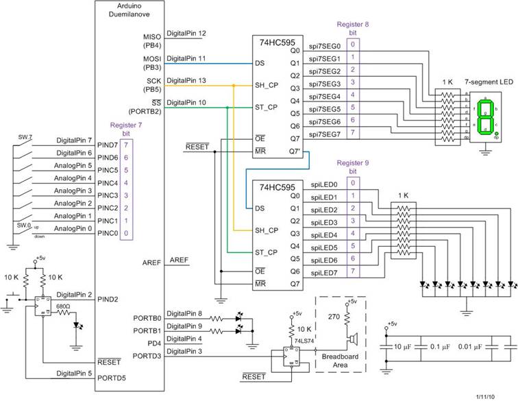
DESIGN EXAMPLE 2 – CSULB Shield Read Switches
Arduino Script
// Analog pins0,1,2,3,4,5 map to Digital pins 14, 15, 16, 17, 18, 19
pinMode(14, INPUT_PULLUP);    // set pin to input with pullup resistor
Repeat this 1 line for pins 15, 16, 17, 18, and 19.
C++
DDRC &= ~0b00111111;
PORTC |= 0b00111111;
Assembly
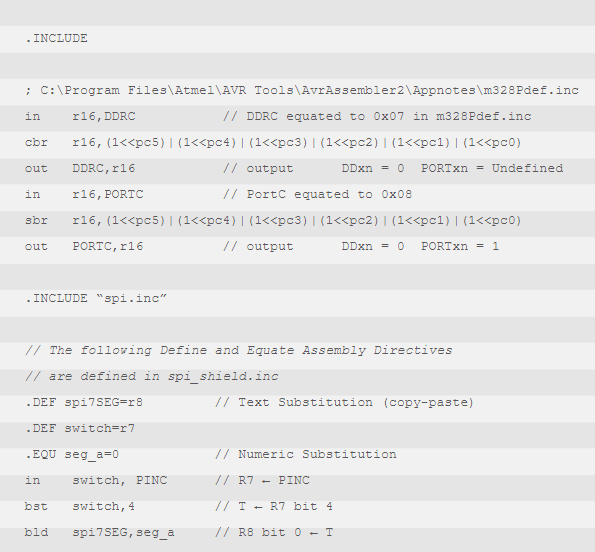
; Initialize Switches with Pull-up resistors

in    r16, DDRC       // Port C DDR for switches 5 to 0
cbr   r16,0b00111111  // define bits 5 to 0 as input (clear)
out   DDRC,r16        // output      DDxn = 0  PORTxn = Undefined

in    r16,PORTC       // PORT C Register for switches 5 to 0
sbr   r16,0b00111111  // add pull-up resistors (PUR)
out   PORTC,r16       // output      DDxn = 0  PORTxn = 1

Main:
  :
in    r7,0x06         // R7 ← PINC
bst   r7,4            // T ← R7 bit 4
bld   r8,0            // R8 bit 0 (seg_a) ← T
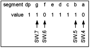
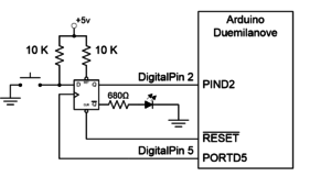
DESIGN EXAMPLE 3 – CSULB Shield Configure D Flip-Flop
Arduino Script
// Variable definitions
const int dff_clk = 5;      // D flip-flop clock wired to digital pin 5
const int dff_Q = 2;        // D flip-flop Q output wired to digital pin 2
                            // Initialize digital pin 5 (dff_clk) as an
                            // output and digital pin 2 (dff_Q) as an input
pinMode(dff_clk, OUTPUT);   // set pin as output
digitalWrite(dff_clk, LOW); // initialize to zero
pinMode(dff_Q, INPUT);      // set pin as input
C++
// Preprocessor directives
#define dff_clk PORTD5
#define dff_Q PIND2

// Initialize push-button debounce circuit
DDRD |= 1 << dff_clk;     // define bit 5 of Data Direction Register
                          //(DDR)PORT D as an output
PORTD &= ~(1 << dff_clk); // initialize to zero
DDRD &= ~(1 << dff_Q);    // define bit 2 of Data Direction Register
                          //(DDR)PORT D as an input
PORTD &= ~(1 << dff_Q);   // without a pull-up resistor
Assembly
; Assembly directives
.EQU dff_clk=PORTD5
.EQU dff_Q=PIND2

; Initialize push-button debounce circuit
  sbi   DDRD, dff_clk   // flip-flop clock, DDRD5 = 1 PORTD5 = Undefined
  cbi   PORTD, dff_clk  //                  DDRD5 = 1 PORTD5 = 0
  cbi   DDRD, dff_Q     // flip-flop Q      DDRD2 = 0 PORTD2 = Undefined
  cbi   PORTD, dff_Q    //                  DDRD2 = 0 PORTD2 = 0
ATmega32U4 Register Summary and the I/O Port
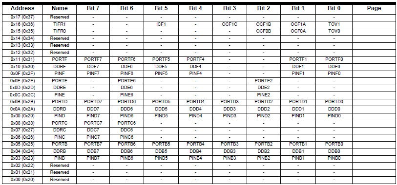
- Three I/O memory address locations are allocated for each port, one each for the Data Register – PORTx, Data Direction Register – DDRx, and the Port Input Pins – PINx.
- The Port Input Pins I/O location PINx is Read Only, while the Data Register and the Data Direction Register are read/write.
- However, Writing a logic one to a bit in the PINx Register, will result in a Toggle in the corresponding bit in the Data Register.
- In addition, the Pull-up Disable – PUD bit in MCUCR disables the pull-up function for all pins in all ports when set.
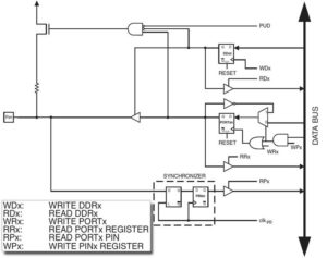
I/O PORT PIN SCHEMATIC
I/O PORT PIN CONFIGURATIONS
Appendix A – PROGRAM I/O PORT AS AN INPUT USING MNEMONICS
In the original Read Switches example, I programmed GPIO Port C bits 5 to 0 as inputs with pull-up resistors. Read GPIO Port C into register r7 and moved bit 4 to register r8 bit 0. In addition the program did not modify Port C bits 7 and 6. In this version, mnemonics and the shift operator are used to increase clarity (i.e., make the code more self documenting).
Appendix B – I/O PORT PIN “SYNCHRONIZER”
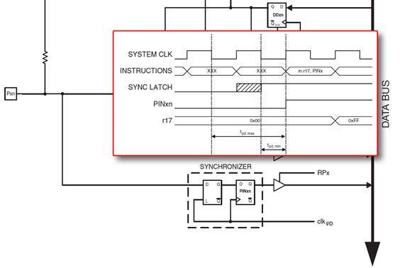
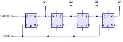
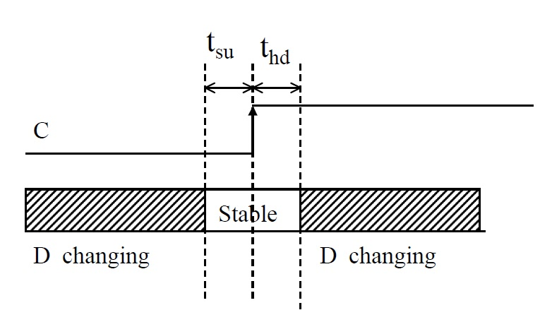
- As previously discussed, you read a port pin by reading the corresponding PINxn Register bit. The PINxn Register bit and the preceding latch constitute a synchronizer. This is needed to avoid metastability if the physical pin changes value near the edge of the internal clock, but it also introduces a delay as shown in the timing diagram.
- Consider the clock period starting shortly after the first falling edge of the system clock. The latch is closed when the clock is low, and goes transparent when the clock is high, as indicated by the shaded region of the “SYNC LATCH” signal. The signal value is latched when the system clock goes low. It is clocked into the PINxn Register at the succeeding positive clock edge. As indicated by the two arrows tpd,max and tpd,min, a single signal transition on the pin will be delayed between ½ and 1½ system clock period depending upon the time of assertion.
Appendix C – SWITCHING BETWEEN I/O PORT PIN CONFIGURATIONS
- When switching between tri-state ({DDxn, PORTxn} = 0b00) and output high ({DDxn, PORTxn} = 0b11), an intermediate state with either pull-up enabled ({DDxn, PORTxn} = 0b01) or output low ({DDxn, PORTxn} = 0b10) must occur.
- Switching between input with pull-up ({DDxn, PORTxn} = 0b01) and output low ({DDxn, PORTxn} = 0b10) generates the same problem. You must use either the tri-state ({DDxn, PORTxn} = 0b00) or the output high state ({DDxn, PORTxn} = 0b11) as an intermediate step.
PWM Motor Speed Control using Timer/Counter 4
This article is on the motor control section of the 3DoT board using Timer/Counter 4 operating in Fast PWM mode.
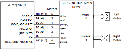
For the remainder of this article use Figure 1 “Atmega32U4 to Motor Driver Interface” to help you cross-reference the tower of babel names used by Atmel, Arduino, and Toshiba (i.e., TB6612FNG).
The direction of motors A and B are defined by inputs AIN1, AIN2, and BIN1, BIN2.
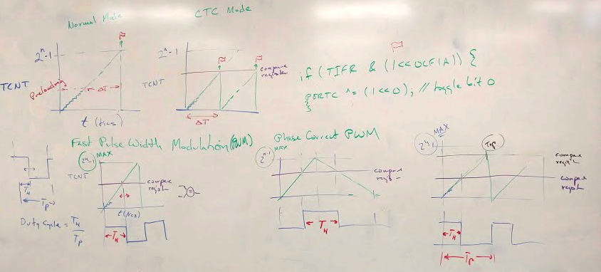
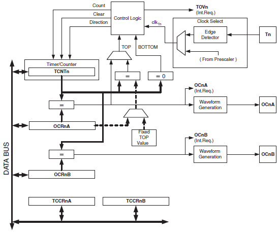
The speed of the motors A and B are controlled by changing the duty cycle of pins PWMA and PWMB respectively. With reference to Figure 1 “ATmega32U4 to Motor Driver Interface,” the speed of motor A will be controlled by Timer 4 register OC4D and motor B by Timer 4 register OC4B. The mnemonic OCnx stands for Output Compare register nx, where n is the Timer number (0, 1, 3, and 4) and x is the Compare register (Timer 4 has four (4) output compare registers designated A, B, C, and D). We will be operating our timer using “Fast Pulse Width Modulation.” I will tell you more about these registers and modes in the coming sections.
Table of Contents [hide]
Reference(s):
- The AVR Microcontroller and Embedded Systems using Assembly and C, by Muhammad Ali Mazidi, Sarmad Naimi, and Sepehr Naimi
Chapter 16: PWM Programming and DC Motor Control in AVR - ATMEL 8-bit AVR Microcontroller with 16/32K Bytes of ISP Flash and USB – ATmega32U4
Chapter 13 “8‑bit Timer/Counter 0 with PWM,” Chapter 14 “16-bit Timers/Counters,” and Chapter 15 “10-bit High Speed Timer/Counter4.”
Motor Direction Control
Figure 1 “Atmega32U4 to Motor Driver Interface” shows that we can configure 2 motors where each motor has 3 control pins and a standby (STBY) pin for the entire IC. If STBY is set low then the motors are not powered regardless of the state of the other two pins. The pins attached to AIN1/2 and BIN1/2 are digital outputs that control the rotation of the motor. The PWM inputs are connect to a pins capable of a PWM output to control the speed of the motor.
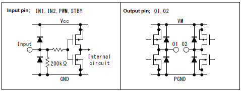
To prevent damage to the internal circuitry of the TB6612FNG, the IC includes clamping diodes on the inputs, a series resistor to limit in-rush current, and a weak pull-down resistor to keep the N-channel MOSFET OFF (Figure 2a Input Circuit). To prevent damage to the output circuitry internal flyback diodes are included (Figure 2b Flyback Diodes). Here is one of many articles on how to use a MOSFET as a Switch which goes into a little more details on these circuit elements.
The direction in which the motors turn are defined in Table 1.
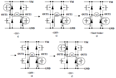
To turn clockwise (CW) you would want to set the H-Bridge to state t1 (see Figure 3 state t1). This would be accomplished by setting PD6 (AIN1) = 1 and PD4 (AIN2) = 0.
PORTD |= _BV(PD6) ;
PORTD &= ~(_BV(PD4));
For a simple “toy” brushed DC motor the magnetic field of the rotor is generated by copper wire wound around a steel-laminate core. The magnetic field is switched by a commutator located on the shaft. The stator uses fixed magnets. The rotor’s copper winding from an electrical perspective is an inductor. During normal operation the back emf generated by the rotor’s winding (an inductor) as it is switched off is routed through a flyback diode (aka flywheel, free wheeling, snubber, suppresser, catch, clamp, kick back).
When switching the motor from CW to CCW care must be taken to not short the MOSFET switches on both legs of the H-bridge while also dissipating the current generated by the collapsing magnetic fields. To solve this problem a Finite State Machine (FSM) is implemented. The controlled transition from one state to the next of the FSM is illustrated in Figure 2 “TB6612FNG H-Bridge states t1 to t5” and Figure 4 “How to program switching between states to prevent short circuit conditions.”
These figures are taken from the TB6612FNG datasheet, and it is the author’s belief that the Toshiba editors made a copy-paste error for states t4 and t5 in Figure 3.
Sample C++ Code to Configure GPIO Ports
Figure 1 is duplicated here for reference purposes.
// MOTOR PINS
// Motor A AIN1,AIN2,PWMA = PD6,4,7
DDRD |= _BV(PD7) | _BV(PD6) | _BV(PD4);      // 0xD0
// Default to low output
PORTD &= ~(_BV(PD7) | _BV(PD6) | _BV(PD4));
// Motor B BIN1,PWMB = PB5,6 and STBY = PB4
DDRB |= _BV(PB6) | _BV(PB5) | _BV(PD4);      //0x70
PORTB &= ~(_BV(PB6) | _BV(PB5 | _BV(PD4)));
// and for motor B BIN2 = PC6
DDRC |= _BV(PC6) ;                           //0x40
PORTC &= ~(_BV(PC6));
Motor Speed Control
Several modulation methods have been developed for applications that require a digital representation of an analog signal. One popular and relevant scheme is pulse width modulation (PWM) in which the instantaneous amplitude of an analog signal is represented by the width of periodic rectangular wave. For example, consider the signals depicted in the figure below. Notice, the PWM version of the signal has a fixed frequency defining the point when a pulse begins. During the period of an individual pulse, the signal remains high for an amount of time proportional to the amplitude of the analog signal.
The speed of our DC motors is controlled using pulse-width-modulation (PWM). But, unlike the sinewave above, where the duty cycle changes after each cycle, we will be controlling the speed of our motors by setting a fixed duty cycle for a given speed. When the rectangular wave signal is high the motor is powered ON, and when the signal is low the power is turned OFF. The speed of the motor is controlled by the fraction of time the controlling signal is ON (duty cycle = Th/Tp %, where Th = time high and Tp = clock period).
ATmega Timer Modes
ATmega, Arduino, and 3DoT PWM Output Pins
Most microcontrollers, including the ATmega family of microcontrollers, provide at least one port that has timer sub-circuitry capable of generating PWM signals on a port pin. Typically, one just needs to configure the frequency and desired duty cycle via a couple of registers. When enabled, the port pin will output a PWM signal that can be demodulated in order to provide an approximation to an analog signal. In our design the characteristics of the motor circuit act to demodulate the PWM signal.
The Arduino Leonardo, on which the 3DoT board is based, can generate rectangular waves for PWM on digital pins 3, 5, 6, 9, 10, 11, 13. The 3DoT supports PWM signals on digital pins 3, 6, 10, 11, and 13.
ATmega32U4 Timing Subsystem
The ATmega32U4 processor has 4 timer/counter (TC) modules that can be used to generate a PWM signal. They are numbered 0, 1, 3, and 4. I will use TCx convention from now on.
Timer/Counter0 is an 8-bit Timer/Counter module, with two independent Output Compare Units, and with PWM support. The Arduino uses Timer 0 to implement the delay(), millis(), and Servo library functions.
Timer/Counter1 and Timer/Counter3 are 16-bit Timer/Counter units with three independent double-buffered Output Compare Units.
Timer/Counter4 is the only 10-bit high speed timer on the ATmega32U4 and has a lot of advanced features, including a high precision mode, double buffering (no glitches), dead time (break before make), fault protection with noise canceling (motor stall monitoring), and even support for brushless dc motors. To keep things simple we will not be using any of these features.
Looking at Figure 1 “ATmega32U4 to Motor Driver Interface” again we see the PWMA and PWMB are associated with OC4D and OC4B respectively. OC4X denotes an output compare with TCNT4. The ATmega32U4 has a more extensive timer system than the ATmega328P and this timer (TCNT4) has 4 Output Compare Registers OCRs attached to it. More on this subject shortly.
What is Fast Pulse Width Modulation
The timing diagram for the fast PWM mode is shown in Figure 15-3. The counter is incremented until the counter value matches the TOP value. The counter is then cleared at the following timer clock cycle. The TCNTn value is in the timing diagram shown as a histogram for illustrating the single-slope operation. The diagram includes the Waveform Output in non-inverted and inverted Compare Output modes. The small horizontal line marks on the TCNTn slopes represent Compare Matches between OCRnx and TCNTx. Figure 15-3 is true for Timer/Counter 4 operation. The only difference for Timer/Counters 0, 1, and 3, is the mnemonic OCWnx, which is replaced simply by OCnx.
The Timer/Counter Overflow Flag (TOVn bit) is set each time the counter reaches TOP. In fast PWM mode, the compare unit allows generation of PWM waveforms on the OCnx pins. In our case OC4D for Motor A and OC4B for Motor B.
Table 15-1 Definitions
For Timer/Counter 4 the OCR4C holds the Timer/Counter TOP value, i.e. the clear on compare match value. The Timer/Counter4 High Byte Register (TC4H) is a 2-bit register[1] that is used as a common temporary buffer to access the MSB bits of the Timer/Counter4 registers, if the 10-bit accuracy is used (Section 15.2.3 Registers). |
[1] Enhanced PWM mode adds an additional 3rd bit to the TC4H register.
PWM Output Frequency
Timer/Counter 4
For Timer/Counter 4 the PWM output frequency can be calculated by the following equation (Section 14.8.3).
I believe the equation defined in Section 15.8.2 “Fast PWM Mode” is incorrect and have replaced with equation used for calculating the frequency throughout the rest of the document.
| Equation 1.0 |
The frequency fOC4X as defined by equation 1 is a function of the system clock (8 MHz), the Prescaler, and TOP. The N variable represents the prescale divider and is defined in TCCR4B CS43:CS40 (stopped, 1, 2, 4,…16384). For our design solutions, N = 1 (no Prescaler) with the 2 bits in TC4H set to zero.,
If we want to replicate the Arduino default frequency of 31.25 kHz, then we would want to keep our TOP, defined by OCR4C, at its default value of 0xFF.
fOC4X = fCLK / 256 = 8 MHz / 256 = 31.25 KHz (approximately 32 kHz)
If we want to replicate the Adafruit Motor Shield version 1 frequency of 64kHz (62.5kHz), then we would set TOP to 0x7F.
fOC4X = fCLK / 128 = 8 MHz / 128 = 62.5 KHz (approximately 64 kHz)
If we really want 64kHz set TOP to 0x7C
fOC4X = fCLK / (1+124) = 8 MHz / 125 = 64 kHz
- At the highest range, the DRV8848 Dual H-Bridge Motor Driver does not support frequencies greater than 250kHz. Another popular motor driver the TB6612FNG does not support frequencies greater than 100kHz.
- At the lowest range, the Adafruit Motor Shield v2 operates at a frequency of 1.6 kHz, due to the limitations of the PCA9865 PWM chip. This frequency is well within the audible range and not recommended.
Calculating the PWM Duty Cycle
We will be operating our 10-bit timer/counter 4 as an 8-bit timer in Fast PWM mode.
- Frequency set by OC4C (TOP) will be defined as 0xFF = 25510
- The most significant 2-bits contained in register TC4H will always be zero.
- TCNT4 will be compared to OCR4D (Motor A) and OCR4B (Motor B).
- Therefore, the Duty Cycle = OCR4x/255, where x equals D or B
10-bit Timer/Counter 4 Register
Timer 4 is a 10-bit timer/counter. Special considerations need to be taken when writing to or reading from a 10-bit register. To write to a 10-bit register, write the most significant 2 bits to TC4H first, followed by the least significant byte (for example TCNT4). The TC4 register is shared by all 10-bit registers in Timer/Counter 4. One consequence of this common register, is that when you read a 10-bit register, the most significant 2-bits are saved to TC4H. Consequently, any subsequent 8-bit write operation to the least significant byte of a 10-bit register, will have this new TC4H value written to the high order bits. Again, this potentially unintended consequence can be avoided by always writing to TC4H first. For more on working with a 10-bit register read Atmel Document 7766 “8-bit AVR Microcontroller with16/32K Bytes of ISP Flash and USB Controller,” Section 15.11 “Accessing 10-bit Register.”
For our robots, the good news is that we never read a 10-bit register. Specifically, the Timer/Counter4 high byte (TC4H) will be always be kept at its default value of zero (0x00).
If you were wondering, TC410 (Bit 2) is an “optional” accuracy bit for 11-bit accesses in Enhanced PWM mode. The enhanced PWM mode allows you to get one more accuracy bit while keeping the frequency identical to normal mode. For more information on this topic see Section 15.6.2 “Enhanced Compare/PWM mode Timer/Counter 4” in the ATmega32U4 Datasheet.
TC4H – Timer/Counter4 High Byte (0xBF)
TCNT4 – Timer/Counter4 (0xBE)
Although Timer 4 is a 10-bit timer/counter, we will be operating it as an 8-bit timer.
Configuring Timing/Counter 4
For our fast PWM implementation we need:
- To enable the Fast PWM Mode
- define output waveform shape
- set an appropriate timer frequency and…
- duty cycle by configuring the OCR registers
Step 1 – Enable Fast PWM mode
Step 2 – Define output waveform shape
PWM Waveform Generation Modes
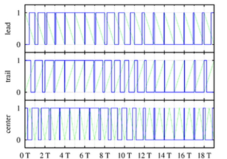
Figure 5 Three types of PWM signals (blue): leading edge modulation (top), trailing edge modulation (middle) and centered pulses (both edges are modulated, bottom). The green lines are the sawtooth waveform (first and second cases) and a triangle waveform (third case) used to generate the PWM waveforms using the intersective method.
Four types of pulse-width modulation (PWM) are possible:
1. The trailing edge can be fixed and the lead edge modulated. ATmega32U4 Timer 4 Fast PWM (PWM4x=1:WGM41..40=00).
2. The leading edge can be fixed and the tail edge modulated. Not implemented on ATmega32U4.
3. The pulse center may be fixed in the center of the time window and both edges of the pulse moved to compress or expand the width. ATmega32U4 Timer 4 PWM Phase and Frequency Correct mode (PWM4x=1:WGM41..40=01)
4. The frequency can be varied by the signal, and the pulse width can be constant. While ATmega32U4 Timers 0,1, and 3 support the CTC mode, Timer 4 does not. Here is an article that shows you how to blink an LED using the CTC Mode (plus how to toggle a bit in C++). In place of the CTC mode, Timer 4 supports two new timer modes, PWM6 / Single slope, and PWM 6 / Dual-slope. These two modes are unique to Timer 4 and are designed for brushless DC motor control.
Timer/Counter4 Control Register A and C – Comparator Output Mode bits
To simplify the definition of the Comparator Output Mode bits located in TCCRA and TCCR4C, I am going to be define COM4D1:0 in TCCR4A. The discussion is directly applicable to the definition of COM4B1:COM4B0 in TCCR4C.
Comparator D Output Mode (COM4D1:COM4D0) TCCR4A bits 3 and 2, control the behavior of the Waveform Output (OCW4D) and the connection of the Output Compare pin (OC4D). If one or both of the COM4D1:0 bits are set, the OC4D output overrides the normal port functionality of the I/O pin it is connected to. The complementary OC4D output is connected only in PWM modes when the COM4D1:0 bits are set to “01”. Note that the Data Direction Register (DDR) bit corresponding to the OC4D pin must be set in order to enable the output driver. The function of the COM4D1:0 bits depends on the PWM4D and WGM40 bit settings. Table 15-17 shows the COM4D1:0 bit functionality when the PWM4D bit is set to a Fast PWM Mode.
Timer/Counter4 Control Register A and C: C++ Code Example
           7654_3210
TCCR4C = 0b0000_1001 = 0x09;
TCCR4A = 0b0010_0001 = 0x21;
//Setting COMD and PWM4D
TCCR4C |= (_BV(COM4D1)| _BV(PWM4D));
TCCR4C &= ~(_BV(COM4D0));
TCCR4A |= (_BV(COM4B1)| _BV(PWM4B));
TCCR4A &= ~(_BV(COM4B1));
Step 3 –Set an appropriate timer frequency
Step 4 –Set the duty cycle by configuring the OCR registers
Calculating the PWM Duty Cycle
As illustrated in Figure 15-4, the 8-bit Timer/Counter Output Compare Registers OCR4x (where x = B or D) are compared with Timer/Counter4. On compare match the OC4x pin is cleared to 0 (see Table 15-17 Compare Output Mode, Fast PWM Mode). Write to this register to set the duty cycle of the output waveform. A compare match will also set the compare interrupt flag OCF4B after a synchronization delay following the compare event.
The Duty Cycle = OCR4x/255, where x equals D or B
OCR4B – Timer/Counter4 Output Compare Register D (Section 15.12.9)
OCR4D – Timer/Counter4 Output Compare Register D (Section 15.12.11)
Timer/Counter4 Output Compare Register: C++ Code Example
// Send argument 'A' for motor A, otherwise motor B selected.
void setPWM(char pin, uint8_t val){
  (pin == 'A') ? (OCR4D = val) : (OCR4B = val) ; // Ternary solution (untested)
}
Fast PWM C++ Code Example
Handling PWM in C++ will be divided into two functions(or sections).
- Configure the Timer and OCR
- Set OCR value as needed to change PWM
void initRobotPWM(){
  // Configure Motor GPIO Port Pins
  // Motor A PD6,4,7
  DDRD |= _BV(PD7) | _BV(PD6) | _BV(PD4);   // 0xD0
  // Default to Low output
  PORTD &= ~(_BV(PD7) | _BV(PD6) | _BV(PD4));

  // Motor B PB5,6 and STBY = PB4
  DDRB |= _BV(PB6) | _BV(PB5) | _BV(PD4);   //0x70
  PORTB &= ~(_BV(PB6) | _BV(PB5 | _BV(PD4)));

  // and for motor B PC6 BIN2
  DDRC |= _BV(PB6) ;                        //0x40
  PORTC &= ~(_BV(PB6));

  // Configure Timer4 for PWMs
  // Motor A on PD7 (OC4D)
  // Motor B on PB6 (OC4B)
  // Ignore 10-bit mode for ease of use

  // Need to configure Timer4 for fast PWM
  // PWM4D and PWM4B set with WGM4 1:0 = 0b00
  // Setting WGM = 00
  TCCR4D &= ~(_BV(WGM41) | _BV(WGM40));
  // Set PD7 and PB6 as outputs
  // I have also added digital pins since they are part of the same system
  // If I want the PWM then I want the digitals also
  // Setting PWM4B and COMB
  TCCR4A |= (_BV(COM4B1)| _BV(PWM4B));
  TCCR4A &= ~(_BV(COM4B1));
  // Setting PWM4D and COMD
  TCCR4C |= (_BV(COM4D1)| _BV(PWM4D));
  TCCR4C &= ~(_BV(COM4D0));

  // SetPrescaler - turn on timer
  // Assumes *Mhz external with default fuses (making Fio = 1Mhz)
  // TB66612FNG says wants PWM Freq <= 100k
  OCR4C = 0xFF;

  // CS4 3:0 = 0b0001;
  TCCR4B |= _BV(CS40);
  TCCR4B &= ~(_BV(CS43)| _BV(CS42)|_BV(CS41)); // Clear prior settings from Arduino.
}
With the configuration ready we can make a function to set our PWM by changing the OCR threshold.
// Send argument 'A' for motor A, otherwise motor B selected.
void setPWM(char pin, uint8_t val){
   (pin == 'A' ) ? (OCR4D = val) : (OCR4B = val) ;  // Ternary solution (untested)
}
Fast PWM Assembly Code Example
The following code example shows how to configure timer/counter 4 for Fast PWM operation, at a frequency of 31.25 KHz.
Reset:
 /* Test code for motor A */
 clr r0          // r0 = 0x00
 clr r1
 com r1          // r1 = OxFF
 /* Test code for motors A and B */
 cbi PORTD, 7    // outputs 0 to Motor A PWM pin when timer/counter 4 disconnected
 cbi PORTB, 6    // outputs 0 to Motor B PWM pin when timer/counter 4 disconnected
                 // see section 15.11 Accessing 10-bit Register
 sts TC4H, r0    // most significant 2-bits
 sts TCNT4, r0   // 10-bit write TC4H:TCNT4 = 0x000
                 // frequency = (8MHz/prescaler)/OCR4C = 31.372 KHz (default)
 sts OCR4C, r1   // 10-bit write TC4H:OCR4C = 0x0FF
                 // duty cycle = OCR4D/OCR4C = 100%
 sts OCR4D, r1   // 10-bit write TC4H:OCR4D = 0x0FF (Motor A)
 sts OCR4B, r1   // 10-bit write TC4H:OCR4B = 0x0FF (Motor B)
 sts TCCR4B, r0  // all configuration bits to default with prescalar = 0, OFF
 ldi r16, 0x09
 sts TCCR4A, r16 // clear to manually control Motors A PWMD
 ldi r16, 0x2
 sts TCCR4A, r16 // clear to manually control Motors B PWMB
 sts TCCR4D, r0  // mode = fast PWM (default)

end of initialization

Walk:
 push r16
 ldi r16, 0x01   // configure inversion mode, reset, dead time to default = 0
 sts TCCR4B, r16 // with prescaler = 1. Motors A and B Timer/Counter 4 ON
 pop r16
 ret

Stop:
 push r16
 clr r16         // configure in fast PWM mode with prescaler = 0
 sts TCCR4B, r16 // Motors A and B Timer/Counter 4 OFF
 pop r16
 ret
Review Questions
- TBD
Answers
Using your mouse, highlight below in order to reveal the answers.
- TBD
Appendix A: Timer/Counter 4 Register Summary
Timer/Counter4 is a monster with five (5) control registers for configuring the timer/counter.
- TCCR4A – Timer/Counter4 Control Register A
- TCCR4B – Timer/Counter4 Control Register B
- TCCR4C – Timer/Counter4 Control Register C
- TCCR4D – Timer/Counter4 Control Register D
- TCCR4E – Timer/Counter4 Control Register E
Two registers used to make the 10-bit timer/counter.
- TC4H – Timer/Counter4 High Byte
- TCNT4 – Timer/Counter4
Four output compare registers
- OCR4A – Timer/Counter4 Output Compare Register A
- OCR4B – Timer/Counter4 Output Compare Register B
- OCR4C – Timer/Counter4 Output Compare Register C
- OCR4D – Timer/Counter4 Output Compare Register D
Two register to support polling and interrupts
- TIMSK4 – Timer/Counter4 Interrupt Mask Register
- TIFR4 – Timer/Counter4 Interrupt Flag Register
And one register unique to timer/counter4
- DT4 – Timer/Counter4 Dead Time Value
Unused Registers
The following registers are not used in our application and are kept at their default values (0x00).
- TCCR4E – Timer/Counter4 Control Register E
- OCR4A – Timer/Counter4 Output Compare Register A
- TIMSK4 – Timer/Counter4 Interrupt Mask Register
- TIFR4 – Timer/Counter4 Interrupt Flag Register
- DT4 – Timer/Counter4 Dead Time Value
Timer/Counter4 Interrupt Mask and Flag Registers (14.10.17, 14.10.19)
The OCF4B and OCF4D flag bits in the TIFR4 register will be set on compare match. As currently configured and defined in section “Timer/Counter4 Control Registers” the OCF4B and OC4D pins are cleared to 0 on compare match.
C++ Arrays, Data Structures, and working with Program Memory
Table of Contents [hide]
Reference(s):
Introduction
In our last C++ lecture we looked at simple datatypes like uint8_t. In this lecture we will be looking at “structured” data types. A structured data type is a collection of related data organized in some logical fashion and assigned a single name (identifier). Data structures may be accessed as a collection of data or by the individual data items that comprise them. Our first structured data type is the array.
C++ simple data types:
- integer (uint8_t, int16_t)
- float (float, double)
- enum
C++ structured data types:
- array
- struct
- union
- class
Arrays
- Arrays are groups of variables of the same data type.
- Variables within the array are organized sequentially and accessed using a simple numerical index. Arrays therefore occupy contiguous locations in memory (SRAM or Flash).
- The first entry has index value 0 and therefore the last entry has an index of “size – 1”, where size is the number of variables within the array.
Declaring Arrays
The simplest array declaration only has a single dimension.
dataType arrayName [ arraySize ];
The arraySize is an integer or constant variable (const int ARRAY_SIZE = 100) greater than zero. The dataType can be any C++ data type.
For example, consider rooms within a maze. Imagine declaring all the variables in the maze as simple data types and then consider how you would access each variable within the maze.
uint8_t room0, room1, room2 ... room99; // a maze with 100 rooms
Clearly, an array provides a much simpler and practical solution. The following C++ statement declares a collection of 100 unsigned 8-bit integers, named maze.
uint8_t maze[100]; // a maze with 100 rooms
Accessing a room within the maze is now as simple as giving its index within brackets []. The use of brackets [] in both the declaration and accessing elements of an array can potentially lead to confusion. In the declaration statement the brackets enclose the size of the array, while in the second case, the brackets enclose the index (base 0).
uint8_t room2 = maze[2];
Initializing Arrays
In C++ we initialize an array using braces {}, also known as curly brackets.
In this example, I want to track a robot’s progress in a maze containing obstacles. For fun the robot looks like a bear and the obstacles are defined as bee stings. As the robot moves from room-to-room the program needs to keep track of 6 variables.
To illustrative purposes, I am going to locate all this data in a single array in SRAM named myRobot containing 6 unsigned 8-bit integers corresponding to these data.
  //                    dir   turn  row   col   room  bees
  uint8_t myRobot[6] = {0x03, 0x00, 0x14, 0x00, 0x00, 0x00};
C++ provides a lot of flexibility in the declaration of an array. However, the array size once defined can not be changed (at least not within the context of an introductory lecture on C++ arrays), nor is this something you want to do in an embedded system. Lets look at two equivalent declaration statements for myRobot.
uint8_t myRobot[]  = {0x03, 0x00, 0x14, 0x00, 0x00, 0x00};  // array holds these 6 bytes
uint8_t myRobot[6] = {0x03, 0x00, 0x14};                    // extra bytes assigned 0x00
As long as the number of values between braces { } is not larger than the number of elements that you declare for the array between the brackets [ ], no error will be generated.
Accessing Array Elements
As mentioned earlier, once an array is initialized, accessing a datum within the array is implemented by placing the index of the datum within square brackets after the name of the array.
uint8_t row = myRobot[2];
The above statement will take 3rd element from the array and assign the value to the row variable. Below is another example that declares, assigns random values, and accesses elements in an array.
void setup ()
{
  Serial.begin(9600);
  // generate random seed based on milliseconds since program started
  randomSeed( (uint8_t) millis()); // cast 32-bit unsigned long to 8-bits
  uint8_t n[10];      // n is an array of 10 8-bit unsigned integers
  // initialize each element of array n to a random number
  for (int i = 0; i < 10; i++) {
    n[i] = random(255);   // random number between 0 and 255
  }
  Serial.print("Element        ");
  Serial.println("Value");
  // output each array element's value
  for ( int i = 0; i < 10; i++) {
    Serial.print("      ");
    Serial.print(i);
    Serial.print("           ");
    Serial.println(n[i]);
  }
}
Here is a sample output.
| Index | Value |
| 0 | 36 |
| 1 | 94 |
| 2 | 54 |
| 3 | 45 |
| 4 | 94 |
| 5 | 170 |
| 6 | 103 |
| 7 | 162 |
| 8 | 3 |
| 9 | 8 |
Example – Running Average
In this example, I will show you how to implement a running average (digital low-pass filter) in your program using an array. It is very useful for inputs that have a high variance between samples (high frequency component), yet only vary slightly over time (low frequency component). An example would be the analog output of an IR sensor as read by the 10-bit ADC peripheral subsystem of an ATmega microcontroller.
Stability and accuracy of the final value will depend on the number of samples used to calculate the running average. If the data changes slowly relative to the sample frequency of the microcontroller, then a larger sample size can be employed.
The example program below reads from an analog pin and computes the running average for a sample size of 8.
Notes:
1. Alternative array initialization includes
window[g_width];
window[g_width] = {};
2. Alternative implementations of limit check on circular buffer include the modulus and “and” operator. The first alternative is not recommended without an fpu. The second alternative requires a buffer size that is a multiple of 2.
n % 8;
n &= 0x000F;
3. You could also use a shift operator in place of division (multiple of 2) Unfortunately, our processor does not have a barrel shifter. Alternative float version: return sum/float(g_width);
C++ Passing Arrays to Functions
C++ does not allow you to pass an entire array as an argument to a function. However, you can pass a pointer to an array by specifying the array’s name without an index.
If you want to pass a single-dimension array as an argument in a function, you will have to declare a pointer to the array as a formal parameter in the function declaration. Here is a quick review of function declarations so that you understand what is being done here.
C++ Function Declarations – Review
When you need to create a custom function that will be used in your program, it must be declared and/or defined. The format for a declaration is shown below.
[Data type of output parameter] [Function Name] ([Data Types of input parameters]) {}
The first part of the function declaration is the data type of the output parameter. This is the type of value that will be returned from the function. This can be an int, float, pointer, or etc. If there is no value to be returned, you will use the void data type. You only need to indicate the data type, as there is no need to name the output.
The second part of the function declaration is the name of the function. This is what is used to call the function. A general convention for naming functions is to have the first word in lowercase and capitalize the first letter of the second word.
The third part of the function declaration are the data types of the input parameters. Any variables or values that the function will need to use must be defined here. This is related to the concept of the scope of a function because copies of those variables or values are created when the input parameters are defined. They are not readily available to the custom functions unless the variables or values have a global scope. It is generally not recommended to use global variables. If there are no inputs, you will have nothing inside of the parentheses.
The final part of a function declaration are the brackets. This is where the function is defined and the code to be performed are placed here. When programming within the Arduino IDE, you will not need to worry about where a function is declared or defined as long as it is located within the main “.ino” file. If a function is called near the beginning of the program and it is defined much later in the code, the compiler will not have an issue with finding the function and will not give a scope error. For this reason, you only need to declare and define a function a single time rather than provide a declaration as part of the header (.h) file, as is the case within traditional C++ IDEs, like Eclipse. Here is an example of a function declaration.
void myFunction(int input1, float input2, char input3) {}
This function is named myFunction and will return no output. It has three input values that are of three different types. The inputs are named input1, input2, and input3 and are only available to be used within the function. There are used more as place holders for the variable or value that you intend to use in the function.
If you are trying to call this example function, you will need to use the following code with the assumption that x is defined as an int, y is defined as a float, and z is defined as a char.
myFunction(x, y, z);
C++ Arguments versus Parameters – Review
Now that we have covered function declarations, it is important to note the distinction between arguments and parameters. A parameter is defined in the function declaration and indicates the type of data that is used. The parameter name is usually a placeholder to represent the kind of value or variable that the function works with. In the function declaration of myFunction the parameters are input1, input2, and input3.
An argument is the actual value or variable being used when a function is called. Arguments are passed to a function and are modified by the function code. From the example above, x, y, and z are the three arguments being sent to myFunction.
Defining A Pointer Parameter
After all of that review, we can now introduce how to define a pointer parameter for a function declaration. There are three ways to do this and all three declaration methods produce similar results because each tells the compiler that an integer pointer is going to be received.
Traditional Way
This form is the general form that has been used the longest and is distinct because of the use of the * to indicate it is a pointer. This is also the most outdated method and should not be used.
void myFunction(int * param) {

 // function definition

}
Modern Way
This is the modern way to define a pointer parameter because it is clear that an array is being used and the intended size of that array is known.
void myFunction(int param[10]) {

  // function definition

}
Modern Way without Bounds Checking
The final method is to define the pointer parameter as an unsized array that can work with any size array argument that is passed to it. As shown in the next example, this way can allow the definition of more general purpose functions. On the minus side, this way can not do bounds checking on your array (i.e., garbage in garbage out).
void myFunction(int param[]) {

 // function definition

}
Now, consider the getAverage function, which takes an array as an argument along with its is size and based on this information returns the average of the numbers contained in the array.
int getAverage(int arr[], int size) {
  int sum = 0;
  for (int i = 0; i < size; ++i) {
    sum += arr[i];
  }
  float avg = float(sum) / size;
  return (int) avg;              // round up
}
Now, lets call the above function.
void setup () {
  // an int array with 5 elements.
  int balance[5] = {1000, 2, 3, 17, 50};
  // pass pointer to the array as an argument.
  int avg = getAverage(balance, 5);  // balance argument is a pointer
  // output the returned value
  Serial.print(“Average value is: ”);
  Serial.print(avg);
}
When the above code is compiled and run, it produces the following result
Average value is: 214
As you can see, the length of the array doesn’t matter as far as the function is concerned because C++ performs no bounds checking for the formal parameters.
Returning an Array from a Function
Just as you can not pass the contents of an array as an argument in a function call, you can not ask a function to return an array, instead you must return a pointer to an array instead. You can do this by defining the data type and using an * to indicate it is a pointer as shown below.
int * myFunction() {}
If the output array is created within the function, qualify the array data type as static, so the pointer being returned is not the address of a local variable that could disappear once the program is out of the scope of the function. What this is referring to is the fact that the program will delete all local variables after it returns from the function (technically the stack frame is destroyed) and the pointer is no longer pointing to the array. By using the static qualifier, it will preserve the data at the address defined by the pointer.
The example shown below will return a pointer to an array of 10 random numbers.
int * getRandom() {
  static int r[10];
  randomSeed( (uint8_t) millis());
  for (int i = 0; i < 10; ++i) {
    r[i] = random(255);  // random number between 0 and 255
    Serial.println(r[i]);
  }
  return r;
}
You can also define a pointer as a variable and initialize its value to be the address of an array. The pointer will need to be the same data type as the array. The example shown below works with the getRandom() function.
int *p;
p = getRandom();
By modifying the pointer, you can access the different elements of the array instead of using the index value. The code below will modify the 2nd element of the array of random numbers to be 20 and the 7th element to be 100.
*(p + 1) = 20;
*(p + 6) = 100;
Structured Data Types in Program Memory (PROGMEM)
Reference:
- Arduino PROGMEM https://playground.arduino.cc/Main/PROGMEM
- Data in Program Space http://www.nongnu.org/avr-libc/user-manual/pgmspace.html
The C++ compiler was designed for computers based on the Princeton memory model. In a Princeton memory model both the program and the data share a common memory, in this case SRAM. Therefore, by default in C++ all arrays are created and stored within SRAM. Many embedded systems, like the AVR family of microcontrollers are based on the Harvard memory model. In a Harvard memory model, the program and data memory reside in different physical memories; specifically, Flash Program and SRAM respectively. To make matters worse, microcontrollers contain significantly more Flash than SRAM memory. For example, the ATmega32U4 contains 32 Kbytes of Flash memory versus only 2.5 Kbytes of SRAM. Therefore, if data in an array is constant and it takes up a lot of space, you should save it all in Flash program memory – but how when the C++ compiler want to put it all in SRAM?
In order to solve this conundrum within the Arduino IDE (GCC C++ compiler), we will be using the avr/pgmspace.h library that is available for the AVR architecture only. It provides definitions for the different data types that can be saved into Flash program memory and all of the functions needed to interact (read, find, compare, etc) with the data saved there. To use the library, you need to add the following line of code with other include statements at the top of the program.
Once it has been included, you can start defining the data to be saved into Flash program memory using the PROGMEM variable modifier. It can be added before the data type of the variable or after the variable name and it indicates that this variable (arrays included) is to be saved in Flash program memory. Below are some examples of how to use it.
const PROGMEM dataType variableName[] = {}; // I like this form
const dataType variableName[] PROGMEM = {}; // this form also works
const dataType PROGMEM variableName[] = {}; // but maybe not this one
- program memory dataType – any program memory variable type
- variableName – the name for your array of data
Rules for initialization of the arrays within Flash program memory are the same as conventional arrays.
const PROGMEM uint8_t myData[11][10] =
{
{0x00,0x01,0x02,0x03,0x04,0x05,0x06,0x07,0x08,0x09},
{0x0A,0x0B,0x0C,0x0D,0x0E,0x0F,0x10,0x11,0x12,0x13},
{0x14,0x15,0x16,0x17,0x18,0x19,0x1A,0x1B,0x1C,0x1D},
{0x1E,0x1F,0x20,0x21,0x22,0x23,0x24,0x25,0x26,0x27},
{0x28,0x29,0x2A,0x2B,0x2C,0x2D,0x2E,0x2F,0x30,0x31},
{0x32,0x33,0x34,0x35,0x36,0x37,0x38,0x39,0x3A,0x3B},
{0x3C,0x3D,0x3E,0x3F,0x40,0x41,0x42,0x43,0x44,0x45},
{0x46,0x47,0x48,0x49,0x4A,0x4B,0x4C,0x4D,0x4E,0x4F},
{0x50,0x51,0x52,0x53,0x54,0x55,0x56,0x57,0x58,0x59},
{0x5A,0x5B,0x5C,0x5D,0x5E,0x5F,0x60,0x61,0x62,0x63},
{0x64,0x65,0x66,0x67,0x68,0x69,0x6A,0x6B,0x6C,0x6D}
};
One trick, I have used in past is to create the array in Microsoft Excel and to export as CSV (Comma delimited) open in Notepad and then copy-paste into the program.
Now that your data resides in Flash program memory, your code to access (read) the data will no longer work![]() The code that gets generated will retrieve the data that is located at the address of the myData array, plus offsets indexed by the i and j variables. However, the final address that is calculated points to the SRAM Data Space
The code that gets generated will retrieve the data that is located at the address of the myData array, plus offsets indexed by the i and j variables. However, the final address that is calculated points to the SRAM Data Space ![]() Not Flash Program Space where the data is actually located. So your program will be retrieving garbage. Again, the problem is that C++ compiler does not intrinsically know that the data resides in the Flash program memory.
Not Flash Program Space where the data is actually located. So your program will be retrieving garbage. Again, the problem is that C++ compiler does not intrinsically know that the data resides in the Flash program memory.
Consequently, you will need to use the pgm_read_byte() or pgm_read_byte_near()functions. From my reading, for AVR microcontroller 16-bit address applications, pgm_read_byte() resolves to pgm_read_byte_near. One way to access the data bytes in the myData 2-dimensional array is by translating the SRAM base + index address into a Flash program memory address using the referencing operator ” .
uint8_t X = pgm_read_byte(&(myData[i][j])); // to learn more about this approach click here.
Here is another way.
uint8_t X = pgm_read_byte(myData + i*10 + j); // to learn more about this approach click here.
In the past I have only worked with one dimensional arrays. Therefore both approaches above are untested.
There are different functions for each of the data types (word, dword, float, and ptr). Click here for more information about these functions and the pgmspace library.
Here is a nice Arduino IDE script showing how to use PROGMEM and the pgmspace library to print out a 1-dimensional array of 16-bit unsigned word values and a text string.
// array of unsigned 16-bit integers
const PROGMEM uint16_t charSet[] = { 65000, 32796, 16843, 10, 11234};

// array of 8-bit characters
const PROGMEM char signMessage[] = {"Hello World"};

char myChar;

void setup() {
 Serial.begin(9600);
 while(!Serial);     // make sure buffer is empty
 // put your setup code here, to run once:
 // read back an array of 2-byte integers
 for (int k = 0; k < 5; k++){
   uint8_t displayInt = pgm_read_word_near(charSet + k);
   Serial.println(displayInt);
 }
 Serial.println();

 // read back an array of char
 int len = strlen_P(signMessage);
 for (k = 0; k < len; k++){
   myChar = pgm_read_byte_near(signMessage + k);
   Serial.print(myChar);
 }
 Serial.println();
}
void loop() {
  // put your main code here, to run repeatedly:
}
Caveats
The macros and functions used to retrieve data from the Program Space generate some extra code in order to actually load the data from the Program Space. This incurs extra overhead in terms of code space (extra machine code instructions) and therefore execution time. Usually, both the space and time overhead is minimal compared to the space savings of putting data in Flash program memory. But you should be aware of this so you can minimize the number of calls within a single function that gets the same piece of data from Flash. It is always instructive and fun to look at the resulting disassembly from the compiler.
Data Structures
Data Structures in C++ provide a greater level of organization for complex systems. Before going into greater details arrays will be reviewed as they give a good insight on how structures work. for example: type array[size]; C++ arrays are a fixed length of a singular data type. This allows us to collect groups of numbers for data for analysis. The issue comes when collections of data are not conducive to arrays or if there is a mixture of data types. Starting from basic C++ foundation, the immediate idea is to make sets of arrays and organize the groups of information by index. That is the core premise of structures! Structures also lays a good foundation as to how Object Oriented Programming (OOP) is organized.
I will take my example from the myRobot array introduced at the beginning of this page. To review, I want to track a robot’s progress in a maze containing obstacles. For fun the robot looks like a bear and the obstacles are defined as bee stings. As the robot moves from room-to-room the program needs to keep track of 6 variables.
As an alternative to working with 6 variables at a time, I created a single array named myRobot containing 6 unsigned 8-bit integers corresponding to these data.
// dir turn row col room bees
uint8_t myRobot[6] = {0x03, 0x00, 0x14, 0x00, 0x00, 0x00};
While consolidating all this data into a single array, accessing the array does not add any clarity to my program. For example, if I wanted to find out the row the robot was in, I would add the code segment myRobot[2] – not very helpful. Data structures allow us to have the best of both worlds ![]()
I will now define a struct named MyRobot_t and group together all the variables we want to keep track of. From our discussion above or group will consist of variables dir, turn, row, col, room, and bees. The generation of this data structure looks like this:
struct MyRobot_t {
  uint8_t dir;
  uint8_t turn;
  uint8_t row;
  uint8_t col;
  uint8_t room;
  uint8_t bees;
}

MyRobot_t Robot
This definition needs to be placed within a header file or else the Arduino IDE will return several errors when we try to use the structure. We will learn more about header files in the future. For example, in Lab 4 the code above is placed in a header file named maze.h. With this structure, we have defined all of our variables as uint8_t but they can be any type. In the main loop, we can create a static structure to hold all of our relevant data.
Wait, we discussed that structs can hold multiple data types but we are holding only one type here. Why not use an array? While you can definitely do the same thing with an array, structs make the code more readable. Now instead of Robot[1] = newTurn;
The instruction would be Robot.turn = newTurn;
Since we need all of our updating functions to have access to the information we will define a static struct inside loop. The struct is now functionally a data type so many of the same rules apply. (const/static/ scope/ etc.) Our Instantiation of the Struct will look like.
void loop() {
  static MyRobot_t Robot{0x03,0x00,0x14,0x00,0x00,0x00};
  // more code
}
This creates a structure called Robot that initializes the values of each variable to the values listed (similar to an array). The list of default values fills the array in the order it was declared in our header file. So for our case dir = 0x03, turn = 0x00 and etc. If you want to be more rigid in your default settings you may define this in the structure prototype as shown below.
In our header…
struct MyRobot_t {
  uint8_t dir  = 0x03;
  uint8_t turn = 0x00;
    .
    .
    .
   etc
}
Object Oriented Programming Example
Class.h File
class sensor {
  private: /* these properties can't be modified outside the class */

  // defined by the constructor
  uint8_t pin;           // IR analog pin (A0, A1, A2, A3)
  float Vref = 3.3;      // analog reference voltage
  uint8_t buffer_depth;  // number of 10-bit ADC samples averaged
  // internal properties // over the data stream. maximum size = 64 (2^6)
  uint8_t pointer = 0;   // index pointer into the buffer
  // points to oldest value
  uint16_t circular_buffer[64] = {0}; // window into the data stream.
  uint16_t sum = 0;     // sum of the readings in the buffer

  public: /* these methods can be called outside the class and can use the private properties */

  // constructor example sensor(A0,8,3.3)
  sensor(uint8_t ic_pin,uint8_t circular_buffer_depth,float voltage_reference){
    pin = ic_pin;
    buffer_depth = circular_buffer_depth;
    Vref = voltage_reference;

    // fill the buffer
    for (int i=0; i < buffer_depth;i++){ readSensor(); } } void readSensor(){ int16_t A_1 = analogRead(pin); // 1. read analog value uint16_t A_0 = circular_buffer[pointer]; // 2. get oldest reading sum += A_1 - A_0; // 3. subtract out oldest reading and // replace with current reading // update circular_buffer circular_buffer[pointer] = A_1; pointer++; if(pointer >= buffer_depth) pointer = 0;
  }

  uint16_t getAvg(){
    return sum/buffer_depth;
  }

  float getVpin(){
    return float(getAvg()) * Vref/1024.0;
  }
};
Arduino Main Page
#include "3DoTconfig.h"
#include "Class.h"

sensor IR_R(A0,8,3.3); // instantiate right IR sensor
sensor IR_L(A2,8,3.3); // instantiate left IR sensor

void setup() {

}

void loop() {
  IR_R.readSensor();

  uint16_t average = IR_R.getAvg();
  float voltage = IR_R.getVpin();

  Serial.print("Average: ");
  Serial.println(average);
  Serial.print("Voltage: ");
  Serial.println(voltage);
  delay(500);
}
Review Questions
- The following code will create an array of how many elements? int testarray[14];
- Write the code that will assign the value of the 3rd element of the array called
balance to a variable called change - Can an array be defined without an array size?
- The action of sending variable values to be used in a function is called what?
- The void data type is used for what?
- Write one of the ways to define a pointer as an input parameter for the function
testFunction() - Write the function definition for a function called returnPointer that has no input
parameters and returns a pointer to an integer - Where are arrays normally saved to?
- What function from the pgmspace library should be used to read a value from an
array? - What type of buffer is required to implement a running average?
Answers
Using your mouse, highlight below in order to reveal the answers.
- 14 elements
- change = balance[2];
- No, all arrays must have a defined size.
- Passing arguments (may need to remove “values” from the question to be less
confusing) - Void is used for defining that a function does not have an output returned
- Void testFunction(int *pointer) {} , void testFunction(int pointer[]) {}, void
testFunction(int pointer[10]) {} - int *pointer returnPointer() {}
- SRAM
- pgm_read_byte_near()
- circular
Appendix A Statistics Package
int readADC(int sensorPin){
int n = 200; // number of ADC samples
int x_i; // ADC input for sample i
float A_1; // current i running average
float A_0; // previous i-1 running average

// rapid calculation method http://en.wikipedia.org/wiki/Standard_deviation
A_0 = 0;
for (int i=1; i <= n; i++){
x_i = analogRead(sensorPin);
A_1 = A_0 + (x_i - A_0)/i ;
A_0 = A_1;
}

// Serial.print(", mean = ");
// Serial.println(A_1);

return (int(A_1));
}
PID Controllers
Table of Contents [hide]
Reference(s):
- AVR221: Discrete PID Controller on tinyAVR and megaAVR devices
- MIT Lab 4: Motor Control introduces the control of DC motors using the Arduino and Adafruit motor shield. A PID controller is demonstrated using the Mathworks SISO Design Tools GUI with accompanying Mathworks PID tutorial “Designing PID Controllers.”
- RepRap Extruder Nozzle Temperature Controller. RepRap provides a feed forward example (PIDSample3) and can be found in the PID_Beta6 project folder.
PID Theory
In Figure 1 a schematic of a system with a PID controller is shown. The PID controller compares the measured process value y with a reference setpoint value, y0. The difference or error, e, is then processed to calculate a new process input, u. This input will try to adjust the measured process value back to the desired setpoint.
The alternative to a closed-loop control scheme such as the PID controller is an open-loop controller. Open-loop control (no feedback) is in many cases not satisfactory and is often impossible due to the system properties. By adding feedback from the system output, performance can be improved.
Unlike a simple proportional control algorithm, the PID controller is capable of manipulating the process inputs based on the history and rate of change of the signal. This gives a more accurate and stable control method.
The basic idea is that the controller reads the system state by a sensor. Then it subtracts the measurement from the desired reference to generate the error value. The error will be managed in three ways, too…
- handle the present, through the proportional term,
- recover from the past, using the integral term,
- anticipate the future, through the derivative term.
Click here to continue the reference article.
From Theory to Programming
The layout in Figure 2 reflects the “classic” PID architecture, naming conventions, and software implementation, versus the primary reference article. Figure 2 shows the PID design by, where Kp, Ki, and Kd denote the time constants of the proportional, integral, and derivative terms respectively. Within the literature, the variable, block, and even layouts may change, while the fundamentals stay the same.
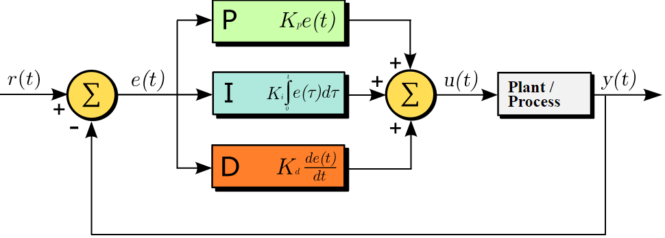
Figure 2. PID controller schematic (cc Arturo Urquizo)
In this section, I am going to step through the blocks defined in Figure 2 “PID controller schematic” and look at how they have been translated into software.
- Error value
- Proportional term
- Integral term
- Differential term
- Summing junction
The software examples are from these PID controllers.
- My Little PID Controller
- Bare Bones (PID) Coffee Controller
- AeroQuad
Error Value
The error value e(t) is defined as the difference between the desired setpoint r(t) and a measured process variable y(t). Here is the C++ statement used by the Bare Bones Coffee control software to implement this term.
  // determine how badly we are doing
  // error = setpoint - process value
  double error = sp - pv;
Proportional Term
The proportional term is only a function of the error. Here is the C++ statement used by the Bare Bones Coffee control software to implement this term.
  // the pTerm is the view from now, the pgain judges
  // how much we care about error we are at this instant.
   double pTerm = kp * error;
The proportional term (P) gives a system control input proportional to the error. Using only P control gives a stationary error in all cases except when the system control input is zero and the system process value y(t) equals the desired value.
In the figure below the stationary error e(t) in the system process value y(t) appears after a change in the desired value r(t). The response shown is that of a second-order transient system. Using a too large P term gives an unstable system.
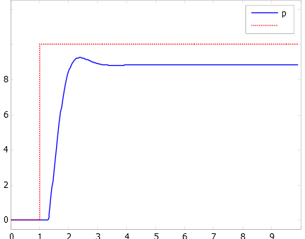
Figure 3. Proportional Term (credit: AVR221: Discrete PID Controller)
Integral Term
You may remember the definition of integration, as shown in Figure 4, from your calculus class. If you have forgotten, the image below was originally presented in this review article. To program the integral term we work backward from the definition by approximating the integral term by taking the area under the error(t) curve.
Here is the C++ statement used by My Little PID control software to implement this term.
 static double iTerm = 0;
 iTerm += ki * error;     // ki unit time (ki = Ki*dT)
Here is the C++ statement used by the AeroQuad PID control software to implement this term. Where the arrow operator -> is used to access the integratedError member of the PIDparameters data structure by reference.
PIDparameters->integratedError += error * G_Dt;
Where global variable for delta time [1] is defined as.
float G_Dt = 0.02;
[1] Of all the PID code examples reviewed for this article, this was the only one that included delta time (Dt). All other code examples combine delta time with the integral term (Ki). This latter approach is computationally more efficient at the cost of clarity (see Computational Simplification).
The figure below shows the step responses to an I and PI controller. As seen the PI controller response has no stationary error and the I controller response is very slow.
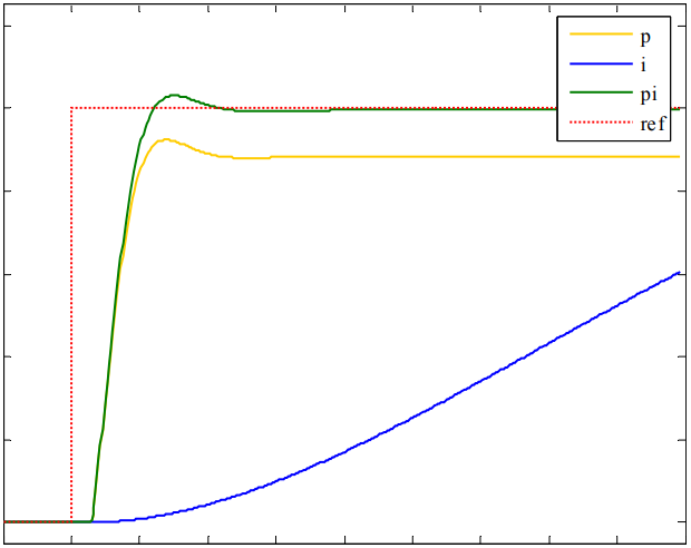
Figure 5. Step Response I and PI Controller (credit: AVR221: Discrete PID Controller)
Differential Term
Returning to your first course in calculus you hopefully also remember the definition of derivative as explained here. To program the differential term we again work backward from the definition by approximating the differential term by finding the slope of the error(t) curve at time t.
Here is a C++ statement for the My Simple PID control software to implement this term.
double dTerm = kd * (pv - last_value); // kd unit time (kd = Kd/dT)
last_value = pv;
Here is a C++ statement, written in the form of the AeroQuad PID control software to implement this term.
PIDparameters->differentialError = (currentPosition - PIDparameters->lastPosition) / G_Dt;
The figure below shows D and PD controller responses. The response of the PD controller gives a faster rising system process value.
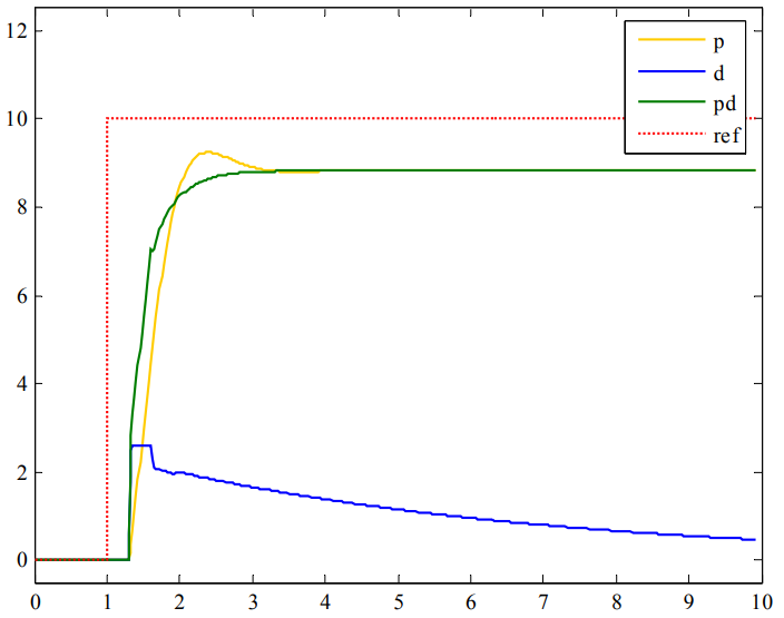
Figure 7. Step Response D of PD Controller (credit: AVR221: Discrete PID Controller)
The differential term essentially behaves as a high pass filter on the system error signal and may therefore increase the effect of noise on the system leading to system instability. To see if a differential term is the best choice for your application, I would recommend reading “The PID’s Derivative Term Can Improve Control Loop Performance, But Often at a Cost.”
Summing Junction
The summing junction u(t) adds the control inputs to be applied to the plant from the Proportional, Integral, and Differential blocks. Depending on the software implementation the gain factors Kp, Ki, and Kd may be added here, or within each computational block. The summing junction is often included in the return statement.
The My Little PID controller takes the former approach as shown here.
return pTerm + iTerm + dTerm; // process input
The Bare Bones Coffee controller takes the former approach as shown here.
  // the magic feedback bit
  return  pTerm + iTerm - dTerm;
The AeroQuad PID controller takes a hybrid approach with the gain factors P and I included at the summing junction, versus the differential block, where the term already includes gain factor D.
return (PIDparameters->P * error) + (PIDparameters->I * (PIDparameters->integratedError)) + dTerm;
The figure below compares the P, PI, and PID controllers. PI improves the P by removing the stationary error, and the PID
improves the PI by the faster response and no overshoot.
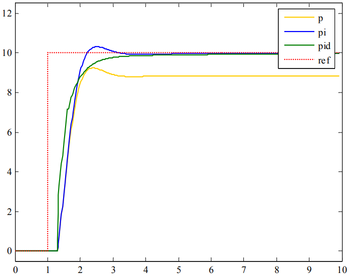
Figure 8. Step Response P, PI, and PID Controller (credit: AVR221: Discrete PID Controller)
Computational Simplification
In moving from theory to program implementation, I intentionally used the AeroQuad as the example for computation of the integral term because it followed directly from the definition of integration and specifically included delta time.
PIDparameters->integratedError += error * G_Dt;
I then took some liberties by creating a differential term that also included time.
PIDparameters->differentialError = (currentPosition - PIDparameters->lastPosition) / G_Dt;
Here is the actual AeroQuad computation of the differential term.
dTerm = PIDparameters->D * (currentPosition - PIDparameters->lastPosition);
The inclusion of the differential gain term D, as mentioned in the discussion of the summing junction, is not unusual; but what happened to time? The better question would surprisingly be, why does the AeroQuad include time in the computation of the integral term in the first place? In almost every software PID controller, time is assumed to be a constant and therefore incorporated into the gain terms to minimize computational time. I was lucky to find one of the few exceptions. To understand why this is true, let’s take a look at a hypothetical PID controller (based on the Bare Bones Coffee controller) where the PID terms include both the gain terms and delta time.
  // iState keeps changing over time; it's
  // overall "performance" over time, or accumulated error
  iTerm += igain * error * dT;
  // the dTerm, the difference between the temperature now
  // and our last reading, indicated the "speed,"
  // how quickly the temp is changing. (aka. Differential)
  dTerm = dgain * (curTemp - lastTemp) / dT;
By application of the associative (iTerm and dTerm) and distributive (dTerm) laws, these two C++ statements could be rewritten as follows.
  iTerm += (igain * dT) * error;
  dTerm = (dgain / dT) * (curTemp - lastTemp);
The answer to our question is now more obvious. To compute the iTerm two multiplication operations are required. In the same way, the dTerm requires division, multiplication, and subtraction. By redefining the gain terms to include the time which we again assume is a constant, the iTerm only requires a single multiplication and the dTerm a single multiplication and subtraction. The Arduino PID library v1.2.1 and My Simple PID controller provides a nice example of this integration of gain terms and time in their tuning function. Here is a simplified version of the SetTunings function.
/* SetTunings(...)*************************************************************
* This function allows the controller's dynamic performance to be adjusted.
* it's called automatically from the constructor, but tunings can also
* be adjusted on the fly during normal operation
* source: Arduino PID Library - Version 1
* by Brett Beauregard <br3ttb@gmail.com> brettbeauregard.com
******************************************************************************/
void setTunings(double Kp, double Ki, double Kd)
  {
    if (Kp<0 || Ki<0 || Kd<0) return;

    double dispKp = Kp;
    double dispKi = Ki;
    double dispKd = Kd;

    double SampleTimeInSec = ((double)dT)/1000;
    kp = Kp;
    ki = Ki * SampleTimeInSec;
    kd = Kd / SampleTimeInSec;
}
Discrete PID Controller – Sample Period
From the last section, we now know that a discrete PID controller will read the error, calculate and output the control input at a constant time interval (sample period dT). So how do I choose a sample time? The sample time should be less than the shortest time constant (36% of normalized output) in the system. This represents the slowest acceptable sample time; hopefully, your system can sample/control the system at a much higher rate.
For PID controllers in which the measurement of the process value y(t) incorporates a gyro (including IMUs) setting the sample period to high will result in an increase in the integration error from the gyro (converting from angular velocity to an angle). Note: this is a different integration than the I in PID.
Read “Improving the Beginner’s PID – Sample Time” by Brett Beauregard, the author of the Arduino PID controller, to learn how time is handled by his PID controller.
Windup
Source: AVR221: Discrete PID controller
When the process input, u(t), reaches a high enough value, it is limited in some way. Either by the numeric range internally in the PID controller, the output range of the controller or constraints in amplifiers, or the process itself. This will happen if there is a large enough difference in the measured process value and the reference setpoint value, typically because the process has a larger disturbance/load than the system is capable of handling, for example, at startup and/or reset.
If the controller uses an integral term, this situation can be problematic. The integral term will sum up as long as the situation lasts, and when the larger disturbance/load disappears, the PID controller will overcompensate the process input until the integral sum is back to normal. This problem can be avoided in several ways. In this implementation, the maximum integral sum is limited by not allowing it to become larger than MAX_I_TERM. The correct size of the MAX_I_TERM will depend on the system and sample time used.
Here is how My Simple PID controller mitigates windup.
static double iTerm = 0;
iTerm += ki * error; // ki unit time (ki = Ki*dT)
iTerm = constrain(windupGuardMin, iTerm, windupGuardMax);
A standard C++ alternative to Arduino’s unique constrain() function is provided here.
if(iTerm > outMax) iTerm= outMax;
else if(iTerm < outMin) iTerm= outMin;
Here is how the Bare Bones Coffee controller mitigates windup.
  // iState keeps changing over time; it's
  // overall "performance" over time, or accumulated error
  iState += error;

  // to prevent the iTerm getting huge despite lots of
  //  error, we use a "windup guard"
  // (this happens when the machine is first turned on and
  // it cant help be cold despite its best efforts)
  // not necessary, but this makes windup guard values
  // relative to the current iGain
  windupGuard = WINDUP_GUARD_GAIN / igain;

  if (iState > windupGuard)
    iState = windupGuard;
  else if (iState < -windupGuard)
    iState = -windupGuard;
  iTerm = igain * iState;
Here is how the AeroQuad controller mitigates windup.
PIDparameters->integratedError += error * G_Dt;
  PIDparameters->integratedError = constrain(PIDparameters->integratedError, -windupGuard, windupGuard);
Where the windupguard is stored in EEPROM and defined here.
float windupGuard; // Read in from EEPROM
Proportional on Measurement
While the integration term is helpful in removing the constant offset error inherent in the proportional controller (you need some error to generate the proportional term in the first place), the I-term itself, even with windup, is a source of error when the setpoint is changed, for example on start-up. In these situations, the integration term will increase up to the windup guard value and must be removed over time. This can only be done by the system overshooting the setpoint (negative error) in order to subtract out the error. The bad news is that all the PID controllers used as case studies will exhibit this behavior. The good news is that the Arduino PID controller version 1.2.1 and later, includes Proportional on Measurement (PonM) tuning, which addresses this problem.
Brett Beauregard, the author of the Arduino PID library, has written an excellent series of articles on the new Arduino PID library. Start with the article entitled “Improving the Beginner’s PID – Introduction.” Clicking the Next>> button at the end of each article will take you in-depth on this PID controller. To learn more about WindUp, read the second article entitled “Improving the Beginner’s PID: Reset Windup.” To learn more about PonM, read the second article entitled “Introducing Proportional On Measurement.”
PID Control Examples
In this section, I am going to look at three control examples.
- Bare Bones (PID) Coffee Controller
- AeroQuad
- Arduino PID library with accompanying Tutorial “Improving the Beginner’s PID: Direction” by Brett Beauregard
The first three control examples are presented in order of the complexity of the PID controller implementation. The coffee controller is a single PID, which can be documented in a single Arduino ino file. The AeroQuad PID software is a modified version of the BBCC: Bare Bones (PID) Coffee Controller with the ability to control multiple control loops. The PID_Beta6 is the Beta version of the Arduino PID library, superseded by PID_v1.
| BBCC | AeroQuad | PID_Beta6 | PID_v1 | |
| Complexity Factor | low | medium | high | high |
| Ability to Change Tunings on the Fly | ? | ? | yes | yes |
| Inputs Normalized | no | no | yes | |
| Input and Output Limits | no | no | yes | |
| Multiple Control Loops | no | yes | yes | |
| Reset-Windup Mitigation | somewhat | somewhat | yes | yes |
| Proportional on Measurement | no | no | no | yes |
| Proportional on Error | yes | yes | yes | yes |
| Derivative Kick | no | no | no | yes |
| Feed forward | no | no | yes | |
| Integration Calculation includes dT | no | yes | no | |
| Tuning | Processing | Labview | Processing |
Like the AeroQuad PID and the coffee controller do not normalize the input. Both include non industrial-standard reset-windup mitigation code. Unlike the AeroQuad PID and Arduino PID library (PID_Beta6), the coffee controller does not calculate the integral term as a function of delta time.
Tuning
Tuning the PID is where most of the “magic wand” action occurs. For some of the software control examples, the term “Configurator” is used for the development environment used for tuning the PID. It is not clear what IDE was used to develop the Configurator used by AeroQuad. The Coffee Controller, like the Arduino Graphical User Interface (GUI), uses Processing as its IDE for developing a simple configurator. The PIDLibrary also used Processing as illustrated here.
Simple Tuning Method
- Turn all gains to 0
- Begin turning up proportional gain until the system begins to oscillate.
- Reduce the proportional gain until the oscillations stop, and then back down by about 20%.
- Slowly increase the derivative term to improve response time and system stability.
- Increase the integral term until the system reaches the point of instability and then back it off slightly.
Ziegler-Nichols method
The Ziegler-Nichols method is outlined in the AVR221: Discrete PID controller article and Jordan’s PowerPoint presentation. The first step in this method is setting the I and D gains to zero, increasing the P gain until a sustained and stable oscillation (as close as possible) is obtained on the output. Then the critical gain Kc and the oscillation period Pc is recorded and the P, I and D values are calculated.
Fitting a simple first order plus dead time dynamic model to process test data.
This tuning method has been ported to the mbed platform. Here is a very nice step-by-step Tuning Example using mbed.
IMC Tuning Method
Since 1942, over one hundred tuning methods have been developed. One of these methods is the Internal Model Control (IMC) tuning method, sometimes called Lambda tuning. This Application Note describes how to tune control loops using IMC tuning rules.
Tuning the Arduino PID Controller
Read “Improving the Beginner’s PID: Tuning” by Brett Beauregard, the author of the Arduino PID controller, to learn how tuning is handled by his PID controller.
PID Control Software Examples
The next three sections, provide the code used for three different PID controllers. To help compare the programs I have color coded the parameters as defined here.
- Summing Junction – Sky Blue
- Proportional Term – Magenta
- Integral Term – Sea Green
- Differential Term – Royal Blue
My Little PID Control Software
/**********************************************************************************************
 * My Little PID Controller - Version 1 *
 * by Gary Hill <hellogaryhill@gmail.com> *
 * March 24, 2021
 *
 * This is a module that implements a PID control loop
 * initialize it with 3 values: Kp,Ki,Kd
 * and then tune the feedback loop with the setP etc funcs
 *
 * This was written based PID controllers by
 * Tim Hirzel
 * Bare Bones Coffee Controller PID
 * http://www.arduino.cc/playground/Main/BarebonesPIDForEspresso#main
 * http://processing.org/
 * Tim Wescott
 * http://www.embedded.com/2000/0010/0010feat3.htm
 * Brett Beauregard <br3ttb@gmail.com> brettbeauregard.com
 * Arduino PID Library
 *
 * All code released under
 * This Code is licensed under a Creative Commons Attribution-ShareAlike 3.0 Unported License.
 **********************************************************************************************/

double kp = 100.0;
double ki = 100.0;
double kd = 100.0;
const double dT = 100.0; // sample time in milliseconds
const double windupGuardMin = 0; // set to output limit
const double windupGuardMax = 255; // set to output limit

void setup() {
  // Initialize serial and wait for port to open:
  Serial.begin(9600);
  while (!Serial) {} // wait for serial port to connect. Needed for native USB port only
}

void loop() {
  static double sp = 0; // set point
  static double updatePID = 0.0;
  if (updatePID >= millis()){
    uint16_t process_value = analogRead(A4); // value 0 - 1023
    double process_input = PID( (double) process_value, sp);
    analogWrite( LED_BUILTIN, (uint8_t) process_input); // value 0 - 255
  }
}

/* Input parameter pv = process value, sp = set point
 * Function returns process input value
 */
double PID(double pv, double sp){
  static double last_value = 0;
  static double i_err = 0;

  double error = sp - pv; // error value
  double pTerm = kp * error; // proportional term

  static double iTerm = 0;
  iTerm += ki * error; // Ki unit time (ki = Ki*dT)
  iTerm = constrain(windupGuardMin, iTerm, windupGuardMax);

  double dTerm = kd * (pv - last_value); // Kd unit time (kd = Kd/dT)
  last_value = pv;

  return pTerm + iTerm + dTerm; // process input
}

/* SetTunings(...)*************************************************************
 * This function allows the controller's dynamic performance to be adjusted.
 * it's called automatically from the constructor, but tunings can also
 * be adjusted on the fly during normal operation
 * source: Arduino PID Library - Version 1
 * by Brett Beauregard <br3ttb@gmail.com> brettbeauregard.com
 ******************************************************************************/
void setTunings(double Kp, double Ki, double Kd)
{
  if (Kp<0 || Ki<0 || Kd<0) return; double dispKp = Kp; double dispKi = Ki; double dispKd = Kd; double SampleTimeInSec = ((double)dT)/1000; kp = Kp; ki = Ki * SampleTimeInSec; kd = Kd / SampleTimeInSec; } /* Tips and Tricks * * You can also update on timer overflow bit associated * with the motors or Arduino built 8-bit timer T0. * By Alexander Littleton, DeRobot 2021 * * For standard C++ alternative to Arduino unique constrain() * if(iTerm > outMax) iTerm= outMax;
 * else if(iTerm < outMin) iTerm= outMin;
 *
 */
AeroQuad PID Control Software
Reference: AeroQuad Downloads
The following AeroQuad header and pde files are key to understanding the AeroQuad PID software.
AeroQuad.h
This header file defines AeroQuad mnemonics
// Basic axis definitions

#define ROLL 0
#define PITCH 1
#define YAW 2
#define THROTTLE 3
#define MODE 4
#define AUX 5
#define XAXIS 0
#define YAXIS 1
#define ZAXIS 2
#define LASTAXIS 3
#define LEVELROLL 3
#define LEVELPITCH 4
#define LASTLEVELAXIS 5
#define HEADING 5
#define LEVELGYROROLL 6
#define LEVELGYROPITCH 7

float G_Dt = 0.02;
DataStorage.h
This header file is used to read and write default settings to the ATmega EEPROM.
// contains all default values when re-writing EEPROM

void initializeEEPROM(void) {

  PID[ROLL].P = 1.2;
  PID[ROLL].I = 0.0;
  PID[ROLL].D = -7.0;
  PID[PITCH].P = 1.2;
  PID[PITCH].I = 0.0;
  PID[PITCH].D = -7.0;
  PID[YAW].P = 3.0;
  PID[YAW].I = 0.0;
  PID[YAW].D = 0.0;
  PID[LEVELROLL].P = 7.0;
  PID[LEVELROLL].I = 20.0;
  PID[LEVELROLL].D = 0.0;
  PID[LEVELPITCH].P = 7.0;
  PID[LEVELPITCH].I = 20.0;
  PID[LEVELPITCH].D = 0.0;
  PID[HEADING].P = 3.0;
  PID[HEADING].I = 0.0;
  PID[HEADING].D = 0.0;
  PID[LEVELGYROROLL].P = 1.2;
  PID[LEVELGYROROLL].I = 0.0;
  PID[LEVELGYROROLL].D = -14.0;
  PID[LEVELGYROPITCH].P = 1.2;
  PID[LEVELGYROPITCH].I = 0.0;
  PID[LEVELGYROPITCH].D = -14.0;

  windupGuard = 1000.0;
FlightControl.pde
This C++ program calls the PID updatePID function and zeroIntegralError subroutine. Here are a few example calls.
updatePID(receiver.getData(ROLL), gyro.getFlightData(ROLL) + 1500, &PID[ROLL]));
updatePID(receiver.getData(PITCH), gyro.getFlightData(PITCH) + 1500, &PID[PITCH]));
updatePID(receiver.getData(YAW) + headingHold, gyro.getFlightData(YAW) + 1500, &PID[YAW]
PID.h
The PID data structure and PID algorithm
struct PIDdata {
  float P, I, D;
  float lastPosition;
  float integratedError;
} PID[8];

float windupGuard; // Read in from EEPROM

// Modified from http://www.arduino.cc/playground/Main/BarebonesPIDForEspresso
float updatePID(float targetPosition, float currentPosition, struct PIDdata *PIDparameters) {
  float error;
  float dTerm;
  error = targetPosition - currentPosition;
  PIDparameters->integratedError += error * G_Dt;
  PIDparameters->integratedError = constrain(PIDparameters->integratedError, -windupGuard, windupGuard);
  dTerm = PIDparameters->D * (currentPosition - PIDparameters->lastPosition);
  PIDparameters->lastPosition = currentPosition;
  return (PIDparameters->P * error) + (PIDparameters->I * (PIDparameters->integratedError)) + dTerm;
}

void zeroIntegralError() {
  for (axis = ROLL; axis < LASTLEVELAXIS; axis++)
  PID[axis].integratedError = 0;
}
Bare Bones (PID) Coffee Controller
As commented on in the code, the AeroQuad PID software is a modified version of the BBCC: Bare Bones (PID) Coffee Controller The coffee controller is a single PID and so is a little simpler to understand.
Like the AeroQuad PID, the coffee controller does not normalize the input. Both include non industrial-standard reset-windup mitigation code. Unlike the AeroQuad PID, the coffee controller does not calculate the integral term as a function of delta time.
(PID_Beta6)
float updatePID(float targetTemp, float curTemp)
{
  // these local variables can be factored out if memory is an issue,
  // but they make it more readable
  double result;
  float error;
  float windupGuard;

  // determine how badly we are doing
  // error = setpoint - process value
  error = targetTemp - curTemp;

  // the pTerm is the view from now, the pgain judges
  // how much we care about error we are at this instant.
  pTerm = pgain * error;

  // iState keeps changing over time; it's
  // overall "performance" over time, or accumulated error
  iState += error;

  // to prevent the iTerm getting huge despite lots of
  //  error, we use a "windup guard"
  // (this happens when the machine is first turned on and
  // it cant help be cold despite its best efforts)
  // not necessary, but this makes windup guard values
  // relative to the current iGain
  windupGuard = WINDUP_GUARD_GAIN / igain;

  if (iState > windupGuard)
    iState = windupGuard;
  else if (iState < -windupGuard)
    iState = -windupGuard;
  iTerm = igain * iState;

  // the dTerm, the difference between the temperature now
  // and our last reading, indicated the "speed,"
  // how quickly the temp is changing. (aka. Differential)
  dTerm = (dgain* (curTemp - lastTemp));

  // now that we've use lastTemp, put the current temp in
  // our pocket until for the next round
  lastTemp = curTemp;

  // the magic feedback bit
  return  pTerm + iTerm - dTerm;
}
PIDLibrary – PID_Beta6.cpp
You will need AVR Studio to view this file with color coding the C++ code.
/* Compute() ******************************************************************
*  This, as they say, is where the magic happens.  this function should
*  be called every time "void loop()" executes.  the function will decide
*  for itself whether a new pid Output needs to be computed
*
*  Some notes for people familiar with the nuts and bolts of PID control:
*  - I used the Ideal form of the PID equation.  mainly because I like IMC
*    tunings.  lock in the I and D, and then just vary P to get more
*    aggressive or conservative
*
*  - While this controller presented to the outside world as being a Reset
*    Time controller, when the user enters their tunings the I term is
*    converted to Reset Rate.  I did this merely to avoid the div0 error
*    when the user wants to turn Integral action off.
*
*  - Derivative on Measurement is being used instead of Derivative on Error.
*    The performance is identical, with one notable exception. DonE causes a
*    kick in the controller output whenever there's a setpoint change.
*    DonM does not.
*
*  If none of the above made sense to you, and you would like it to, go to:
*  http://www.controlguru.com.  Dr. Cooper was my controls professor, and
*  is gifted at concisely and clearly explaining PID control
******************************************************************************
*/

void PID::Compute()
{
  justCalced=false;
  if (!inAuto) return; //if we're in manual just leave;
  unsigned long now = millis();
  //millis() wraps around to 0 at some point. depending on the version of the
  //Arduino Program you are using, it could be in 9 hours or 50 days.
  //this is not currently addressed by this algorithm.
  //...Perform PID Computations if it's time...

  if (now>=nextCompTime)
  {

    //pull in the input and setpoint, and scale them into percent span
    double scaledInput = (*myInput - inMin) / inSpan;
    if (scaledInput>1.0) scaledInput = 1.0;
    else if (scaledInput<0.0) scaledInput = 0.0;

    double scaledSP = (*mySetpoint - inMin) / inSpan;
    if (scaledSP>1.0) scaledSP = 1;
    else if (scaledSP<0.0) scaledSP = 0;

    //compute the error
    double err = scaledSP - scaledInput;

    // check and see if the output is pegged at a limit and only
    // integrate if it is not. (this is to prevent reset-windup)
    if (!(lastOutput >= 1 && err>0) && !(lastOutput <= 0 && err<0))
    {
      accError = accError + err;
    }

    // compute the current slope of the input signal
    // we'll assume that dTime (the denominator) is 1 second.
    double dMeas = (scaledInput - lastInput);
    // if it isn't, the taud term will have been adjusted
    // in "SetTunings" to compensate
    //if we're using an external bias (i.e. the user used the
    //overloaded constructor,) then pull that in now
    if(UsingFeedForward)
    {
      bias = (*myBias - outMin) / outSpan;
    }

    // perform the PID calculation.
    double output = bias + kc * (err + taur * accError - taud * dMeas);

    //make sure the computed output is within output constraints
    if (output < 0.0) output = 0.0;
    else if (output > 1.0) output = 1.0;
    lastOutput = output;     // remember this output for the windup
                             // check next time
    lastInput = scaledInput; // remember the Input for the derivative
                             // calculation next time
    //scale the output from percent span back out to a real world number
    *myOutput = ((output * outSpan) + outMin);
    nextCompTime += tSample;  // determine the next time the computation
                              // should be performed
    if(nextCompTime < now) nextCompTime = now + tSample;
    justCalced=true;  //set the flag that will tell the outside world
                      // that the output was just computed
  }
}
PID Controller for Line Following Robots
By Jordan Smallwood | October 4th, 2017
Overview
The following PowerPoint presentation introduces Proportional Integral Derivative (PID) controllers and their application to a line following robot. The presentation concludes with an in-depth look with examples of integration into a line following robot in C++.
References
- https://en.wikipedia.org/wiki/PID_controller
- https://www.cds.caltech.edu/~murray/courses/cds101/fa04/caltech/am04_ch8-3nov04.pdf
Review Questions
- To Be Written
Answers
Using your mouse, highlight below in order to reveal the answers.
- To Be Written
ATmega Analog-to-Digital Conversion
Table of Contents [hide]
Reference(s):
- The AVR Microcontroller and Embedded Systems using Assembly and C by
Muhammad Ali Mazidi, Sarmad Naimi, and Sepehr Naimi, Chapter 13 ADC, DAC, and Sensor Interfacing - ATMEL 8-bit AVR Microcontroller with 4/8/16/32K Bytes In-System Programmable Flash, Chapter 23 “Analog-to-Digital Converter”
- AVR Freaks Newbie’s Guide to the AVR ADC by Ken Worster
- Successive Approximation ADC, Georgia State University, Department of Physics and Astronomy
- Successive approximation ADC, Wikipedia
ATmega MCU ADC Subsystem Features
- 10/8-bit Resolution
- 0.5 LSB Integral Non-linearity
- ± 2 LSB Absolute Accuracy
- Temperature sensor
- Single Conversion, Free Running, and 3DoT Mode 8
- Interrupt on ADC Conversion Complete
- Optional Left Adjustment for ADC Result Readout
- 2.56 V ADC Reference Voltage
- Up to 15 kSPS at Maximum Resolution with a conversion times of 13 μs (ATmega328P) and 65 – 260 μs (ATmega32U4)
- Six (ATmega328P), twelve (ATmega32U4), and five (3DoT) Multiplexed Single-Ended Input Channels
- One Differential amplifier providing gain of 1x – 10x – 40x – 200x (ATmega32U4 only)
- Sleep Mode Noise Canceler (ATmega32U4 only)
How it Works
What is a Successive Approximation ADC?
Illustrations from Tocci, Ronald J., Digital Systems, 5th Ed, Prentice-Hall, 1991.
A successive approximation ADC is a type of analog-to-digital converter that converts a continuous analog waveform into a discrete digital representation via a binary search through all possible quantization levels before finally converging upon a digital output for each conversion.
The successive approximation Analog to digital converter circuit typically consists of four chief subcircuits. Figure 1 is an example 4-bit ADC and will be used to illuminate how these four subcircuits work together to convert an analog value into a digital number.
- A sample & hold comparator circuit acquires the analog input voltage (Vs) and compares it to the output of an internal DAC with input reference voltage (Vref). To keep the illustration as simple as possible, this reference voltage is not shown and may be assumed to be equal to 15 v. In our example 4-bit DAC the analog input voltage (Vs) is set to 7.2 volts.
- The result of the comparison is sent to a successive approximation register (SAR). Identified as control logic and bits D3 to D0 in our simplified 4-bit DAC block diagram.
- The internal DAC supplies the comparator with an analog voltage equivalent of the digital code output of the SAR for comparison with Vs.
- The SAR subcircuit, a finite state machine, implements the algorithm defined in Figure
Using the Built-in ADC in the ATmega MCU
The ATmega datasheet provides everything you need to know to use the ADC subsystem of our AVR microcontroller. In the following sections I am going to focus on those topics which I consider to be most relevant when wanting to use the ADC:
- How to connect the pins related to the ADC (Voltage Reference).
- How to make an Analog to Digital conversion within the Arduino IDE.
- A Simple Analog to Digital Conversion (analogRead)
- The registers of the ADC (ADMUX, ADCSRA, and ADCH:ADCL). ADC registers ADCSRB and DIDR0 are left at default values and considered outside the scope of this introductory lesson.
- How to select an operating mode (Single Conversion and Free-Running)
- How to specify resolution/conversion speed (Sample Frequency).
- How to verify conversion complete (polling the ADSC bit).
I have tried to weave these topics into a single story centered around the ATmega32U4 and the Arduino analogRead function. Consequently, section headings are more for future reference and for the most part can be ignored if you are reading the material from beginning to end.
Any good story must start with the big picture and ours is no exception. In Figure 3 we have the block diagram of the ADC subsystem of the AVR microcontroller.
Note: ADCSRA ADATE signal mislabeled as ADFR in Figure 3.
Voltage Reference (VREF)
While most of our story centers around how to work with the registers of the ADC. In this section I am going to talk about how the Arduino hardware handles the reference voltage for the 10-bit DAC (AVCC to VREF), how you can improve the noise immunity of your design, and finally how you can change the reference voltage (AVCC to Vref). If you choose to do the latter, make sure you read the warning (or have a spare ATmega32U4 on hand).
The minimum value of the 10-bit output of the ADC register (0x000) represents GND and the maximum value (0x3FF) represents the voltage on the VREF line, within 1 LSB. You can think of VREF as normalizing the input voltage as defined by the following equation.
If you want to get into the details, I would recommend reading “An ADC and DAC Least Significant Bit (LSB)” by Adrian S. Nastase.
The source of the reference voltage is set by bits REFS1 and REFS0 in the ADC Multiplexer Select (ADMUX) register as defined in Table 1.
As shown in Table 1, the reference voltage to the 10-bit DAC can be sourced from an external AREF source, AVCC, or an internal 2.56V reference voltage.
3DoT Hardware Implementation of AVCC and AREF
We are using the 3DoT board and so are limited by how they have wired these pins. Comparing this schematic with Figure 24.7.2 “ADC Power Connections” in the Reference Data Sheet of the ATmega32U4, we see that this is not the optimal wiring solution with missing 100nF capacitor from AVCC to analog ground.
For voltage reference mode 012 and 112 (Table 1) Microchip recommends an external 0.1 uF capacitor be connected from AREF pin to analog ground to improve noise immunity. As seen in Figure 4 “How the 3DoT wires the ADC reference voltage pins” schematic, the 3DoT board comes with with a 0.1 uF capacitor to ground and a Ferrite Bead, the Arduino UNO does not come with either.
Arduino IDE Software Implementation of AVCC and AREF
The default setting for an analogRead call within the Arduino IDE sets ADMUX bits REFS1 = 0, and REFS0 = 1. Looking at Table 1 and the 3DoT schematic (Figure 4), we see that the Arduino IDE therefore defaults to a ADC reference voltage of 3.3v.
Changing the Reference Voltage
The Arduino provides a function named analogReference(uint8_t mode) which allows you to change the DEFAULT value of voltage reference source (REFS = 0b01)
void analogReference(uint8_t mode)
{
  // can't actually set the register here because the default setting
  // will connect AVCC and the AREF pin, which would cause a short if
  // there's something connected to AREF.
  analog_reference = mode;
}
Also included in the wiring.h header file are the three available values defined as constants (compare names below to Table 1).
#define EXTERNAL 0
#define DEFAULT 1
#define INTERNAL 3
For example, if you want to reference an external voltage wired to the AREF pin you would add the following code to the setup section of your Arduino sketch. In this example, AREF is wired to the 3.3 V output provided by the Arduino.
analogReference(EXTERNAL); // Vref wired to 3DoT shield AREF pin
WARNING: If you wire a voltage source directly to AREF, when the Arduino changes the ATmega32U4 default setting of 0b00 to the Arduino’s default value of 0b01, a short will exist between AVCC and AREF lines as shown in Figure 3. Even though your setup script will switch it back to its original safe 0b01 value the damage will already have been done to the ATmega32U4 (i.e., time to buy a new microcontroller). To protect the ATmega32U4 during this short period of time, add a 1K ohm resistor between your reference voltage source and the AREF pin. During normal operation the voltage drop across this resistor should be negligible.
How to make an Analog to Digital conversion within the Arduino IDE
Converting an Analog signal into its digital equivalent is accomplished within the Arduino IDE using the analogRead(pins) function. The analogRead function takes a single argument “pin”, identifying one out of the five Analog pins of the 3DoT to be read.
Using the analogRead function is demonstrated by the AnalogInput sketch (Open – Analog – AnalogInput)
/*
 Analog Input
 Demonstrates analog input by reading an analog sensor on analog pin 0 and
 turning on and off a light emitting diode(LED) connected to digital pin 13.
 The amount of time the LED will be on and off depends on
 the value obtained by analogRead().

 The circuit:
 * Potentiometer attached to analog input 0
 * center pin of the potentiometer to the analog pin
 * one side pin (either one) to ground
 * the other side pin to +5V
 * LED anode (long leg) attached to digital output 13
 * LED cathode (short leg) attached to ground

 * Note: because most Arduinos have a built-in LED attached
         to pin 13 on the board, the LED is optional.

 Created by David Cuartielles
 Modified 16 Jun 2009
 By Tom Igoe
 http://arduino.cc/en/Tutorial/AnalogInput

 */

int sensorPin = 0;   // select the input pin for the potentiometer
int ledPin = 13;     // select the pin for the LED
int sensorValue = 0; // variable to store the value coming from the sensor

void setup() {
  // set pin(s) to input and output
  pinMode(sensorPin + A0, INPUT);
  // declare the ledPin as an OUTPUT:
  pinMode(ledPin, OUTPUT);
}

void loop() {
  // read the value from the sensor:
  sensorValue = analogRead(sensorPin);
  // turn the ledPin on
  digitalWrite(ledPin, HIGH);
  // stop the program for  milliseconds:
  delay(sensorValue);
  // turn the ledPin off:
  digitalWrite(ledPin, LOW);
  // stop the program for for  milliseconds:
  delay(sensorValue);
}
In the next section we will look at how the analogRead function works. Our story is about to become a lot darker.
A Simple Analog to Digital Conversion
Before we get into the details of how the Arduino analogRead function works let me give you a thumbnail sketch of the process. If you find yourself getting lost in the forest, you may want to reread the following paragraph. Figure 5 “ADC Registers” is provided here to help you through the mnemonic soup (ADSC, ADCSRA, etc.) contained in this summary paragraph.
The Arduino analogRead function performs a simple analog conversion, where the ADC is triggered manually by setting the ADSC bit to logic one in the ADCSRA register. The ADSC bit will read as logic one as long as a conversion is in progress. When the conversion is complete, it returns to zero. The analogRead function polls this bit and returns the 10-bit result in the ADCH:ADCL register pair when conversion is complete.
Now, let’s take a look under-the-hood at the Arduino analogRead function. I am assuming the use of the Arduino compatible 3DoT board. Consequently, to simplify the explanation of this function I have removed a macro expansion required by the Arduino MEGA.
int analogRead(uint8_t pin)
{
  uint8_t low, high;

  // set the analog reference (high two bits of ADMUX) and select the
  // channel (low 4 bits). this also sets ADLAR (left-adjust result)
  // to 0 (the default).
  ADMUX = (analog_reference << 6) | (pin & 0x0f);

  // without a delay, we seem to read from the wrong channel
  //delay(1);

  // start the conversion
  sbi(ADCSRA, ADSC);

  // ADSC is cleared when the conversion finishes
  while (bit_is_set(ADCSRA, ADSC));

  // we read ADCL first; doing so locks both ADCL
  // and ADCH until ADCH is read. reading ADCL second would
  // cause the results of each conversion to be discarded,
  // as ADCL and ADCH would be locked when it completed.

  low = ADCL;
  high = ADCH;

  // combine the two bytes
  return (high << 8) | low;
}
Exercise 1: The C++ sbi instruction is now deprecated. Write one line of C++ code to replace this instruction.
The Registers of the AVR ADC Subsystem
Although the ADC subsystem of the ATmega32U4 microcontroller contains seven (7) registers (see Figure 5), only ADMUX, ADCSRA, ADCH, are ADCL are used to the configure the ADC as used by the Arduino analogRead function. We will look at ADCSRB, DIDR0 and DIDR2 shortly.
ADC Multiplexer Selection Register Initialization
Assuming the unsigned 8-bit argument pin in the analogRead(pin) function call is zero (0016), the C++ line…
ADMUX = (analog_reference << 6) | (pin & 0x0f);
…at the beginning when the Arduino bootstrap loader initializes the Analog subsystem of the ATmega32U4 microcontroller, the ADC ADMUX register is set to 0100_00002.
Let’s take a closer look at each of these bits and what part they play in our story.
As originally covered in the “Voltage Reference” section of our lesson and summarized in Table 1 “Voltage Reference Selections for ADC”, setting REFS1 = 0 and REFS0 = 1 means that our reference voltage VREF is equal to VCC, which we will assume is 3.3v.
The ADC generates a 10-bit result which is stored in the ADC Data Registers, ADCH and ADCL. By default, the result is presented right adjusted (ADLAR = 0), but can optionally be presented left adjusted by setting the ADLAR bit in ADMUX to logic one. For the analogRead function the result of the conversion process is right adjusted (DEFAULT value).
Exercise 2: Add unsigned 8 bit integer parameter left_adjust to the analogRead function (i.e, analogRead(uint8_t pin, uint8_t left_adjust). Use left_adjust to set or clear the ADLAR bit in ADMUX. Your function should insure all undefined bits of the ADLAR argument (bits 7 to 1) are set to zero.
Using Different Channels as seen from the Figure 3 schematics, the ADC can access multiple analog channels through the MUX. The ADMUX Register controls the MUX and the different input pins which can be directed to the sample-hold circuit. The sample-hold circuit keeps the sampled voltage level stable while the conversion is made, using successive approximation. The analogRead functions pin parameter allows the calling program to define which pin is to be read. The 3DoT board uses the ATmega32U4 processor packaged in a TQFP (See Figure 1-1 “Pinout ATmega16U4/ATmega32U4” in the data sheet). This limits us to 12 analog inputs. Of these 12 possible ADC inputs, the 3DoT makes available 5 (ADC5:ADC0). For my example, the analog signal is read on pin ADC0. Consequently, the input to the MUX is set to 0 (MUX3 = 0, MUX2 = 0, MUX1 = 0, MUX0 = 0).
ADC Control and Status Register A Initialization
During initialization (see init() subroutine in main(void)), the Arduino sets ADCSRA to 1000_01112.
The bits of the ADCSRA register are used to set the operating mode and sample frequency of the ADC. We will look at the “single conversion” and “free-running” modes of operation. These are the two most common operating modes, although there are others. For example you can program the ADC to sample an analog line at a fixed interval of time.
How to select an operating mode
Single Conversion Mode
Before starting a conversion the ADC must be enabled. This is done by setting the bit ADEN = 1 in the ADCSRA Register. As illustrated in Figure 7 this is taken care of by Arduino init() subroutine.
The ADC can be run in two modes: Single Conversion mode or Free-running mode. In Single Conversion mode the conversion is initiated manually, by setting the ADSC bit in the ADCSR Register. Arduino’s analogRead function uses the single conversion mode as shown in the following inline assembly instruction.
  // start the conversion
  sbi(ADCSRA, ADSC);
Free-Running Mode
One of the disadvantages of the Arduino IDE is that we trade flexibility for simplicity. To run the ADC in Free-Running mode it may be best to make your own custom version of analogRead or to write your own ADC C++ within a more powerful IDE like Eclipse, AVR Studio, or ATMEL Studio.
Note: The Analog Comparator Multiplexer Enable ACME bit is not used by the ADC circuit and should be kept at its default value of 0.
In Free-Running mode the ADC is setup to start a new conversion immediately after the previous conversion is complete. To enable this feature, the ADC Auto Trigger Enable ADATE bit in ADCSRA (Figure 7) is set to one and ADC Auto Trigger Source ADTS[3:0] bits in ADCSRB (Figure 8) are set to zero. This selects the ADC interrupt flag ADIF as the trigger source. The ADC now operates in Free Running mode, constantly sampling and updating the ADC Data Registers.
The first conversion is started by writing a logical one to the ADSC bit in ADCSRA. If you use this mode, I would recommend enabling the I-bit in SREG and ADC Interrupt (ADIE = 1) bit in ADCSRA. Now your Interrupt Service Routine (ISR) can take action each time a conversion is complete (no more polling).
3DoT Mode 8
In addition to the free running mode, the ATmega32U4 can automatically start an ADC conversion based on a number of events, as defined in Figure 9 “ADC Auto Trigger Source Selections.” Of particular interest to 3DoT robots is mode 8 “Timer/Counter4 overflow.” The frequency of the PWM signal, which sets the motor speed of a 3DoT robot, is defined by Timer4. Therefore, by using this mode, a 3DoT robot can be taught to read a sensor only when it can take action (i.e., change the speed of its motors). Further, as discussed in Section 24.7.2 “Analog Noise Canceling Techniques” of the ATmega32U4 datasheet, ff any ADC port pins are used as digital outputs, it is essential that these do not switch while a conversion is in progress. Both PWM pins which drive the 3DoT motors are shared with Analog channels, by operating in Mode 8 and assuming a realistic duty cycle (motors not stalled), this restriction can be met.
How to specify resolution/conversion speed (Sample Frequency)
The sample frequency of the AVR ADC is a function of the operating mode (single conversion, free-running mode 8), the ATmega32U4 system clock frequency (CK = 8 MHz), and the prescale setting (ADCSRA bits ADPS2 to ADPS0).
From when a single conversion is initiated to the result is in the ADCH:ADCL Registers 13 ADC cycles will pass as defined in Table 2.
The “First conversion” line refers to when the ADEN bit in ADCSRA register is set. This additional time is required to initialize the analog circuitry including the 7-bit ADC prescaler (see Figure 10 “ADC Prescalar”). The Arduino sets the ADEN bit in the init() subroutine.
By default, the successive approximation circuitry requires an input clock frequency between 50 kHz and 200 kHz to get maximum resolution. If a lower resolution than 10 bits is acceptable, the input clock frequency to the ADC can be higher than 200 kHz to get a higher sample rate. The Arduino init() routine sets prescaler bits ADPS2 to ADPS0 in the ADCSRA Register to all ones (see Figure 7) setting the prescaler to 128. Which means that:
fADC = fCK/128 = 8 MHz/128 = 62.5 kHz
Consequently, the ADC prescaler of the ATmega32U4 generates an ADC clock frequency of 62.5 kHz (less than 200 kHz). By setting the ADC prescaler to 64 (ADPS = 0b110) we can reach a conversion frequency of 125 kHz (again less than 200 kHz), giving us a maximum resolution of 10 bits at a sample frequency of:
fsample = fADC / 13 = 9.615 ksps (104 μs Conversion Time)
This topic is covered in any number of forum posts including “How do I know the sampling frequency?”
Each conversion starts on a rising edge of the ADC clock, and at least one ADC clock cycle is lost executing code. So yes, 8928.6 Hz is the fastest you can get by calling in a tight loop, v.s. a very consistent 9615.4 Hz in free-running mode. – Edgar Bonet Nov 14 ’19 at 14:46
An ADC clock at 250 kHz violates the limit in ADC clocking for full 10 bit resolution (ADC clock 200 kHz for 10-bit resolution). So what would happen if we set our prescaler to divide the system clock by 32 or less? Fortunately, the “Open Music Labs” has done some in depth research and testing to answer this specific question. Table 3 “ATmega ADC resolution versus clock frequency” provides a quick answer; however, I recommend you read the article before trying this at home. From reading the article, you will discover that setting the correct bits in the DIDR register, plays a critical role in improving accuracy.
Working form Table 3, it is shown that a prescaler of eight (8) sets the ADC clock frequency to 1 MHz with a corresponding maximum sample rate of 74.074 ksps (Free-Running mode), with a resolution of an 8-bit ADC.
How to verify conversion complete (polling the ADSC bit)
When we last left our Arduino analogRead routine, it had started the analog to digital conversion process by setting the ADEN bit in the ADCSRA Register to logic one.
// start the conversion
sbi(ADCSRA, ADSC);
The analogRead routine now polls the ADSC bit in the ADCSRA register within a C++ while loop.
// ADSC is cleared when the conversion finishes
while (bit_is_set(ADCSRA, ADSC));
Once the conversion is complete, the ADC hardware subsystem of the ATmega328P clears the ADSC bit and stores the result in the ADCH:ADCL register pair.
It is important to read ADCL first to ensure that valid data is read. By reading ADCL first, the ADCL and the ADCH Registers are “locked” and cannot be updated by the ADC until the ADCH has been read.
low = ADCL;
high = ADCH;
Our story is finally over, when the high order byte is shifted 8 places to the left and or’d with the low order byte. The 10 bit answer (zero extended to 16 bits) is now returned as a positive integer (16-bit signed).
// combine the two bytes
return (high << 8) | low;
DIDRn – Digital Input Disable Register 0 and 2
Although it does not play a part in the Arduino IDE, your own design should initialize the DIDR0 register, as defined here.
When an analog signal is applied to the digital input buffer of a GPIO port pin, the buffer can consume an unnecessarily high rate of current as the input signal voltage stays within the undefined region between logic one and zero (see slew rate). To solve this problem, pins used as analog inputs should have their corresponding digital pins disabled. Specifically, set the corresponding bit in DIDRn to one. So how does this apply to the 3DoT board?
The 3DoT board can read from 1 to 6 Analog channels as defined in Figure 13 “3DoT Analog Inputs.” Comparing Figures 12 and 13, it is clear that DID2 may be left at its default values (cleared). Conversely, the 3DoT board reads the battery level on ADC0D, DIDR0 bit 0. Consequently, this bit should always be initialized to logic 1. The remaining DIDR0 bits should be set or cleared based on the robot architecture.
Concluding Remarks
As we have seen, the Arduino analogRead function provides a simple way for converting an analog signal into its digital equivalent. In EE470 “Digital Control” the experimentally measured conversion time of the analog_wire_spi.ino script is 125 ?sec (sample frequency = 8 ksps). From our discussion, we know that the conversion time of our Arduino script is 104 ?sec. One thing we can take away from this finding is that over 83% of the time the script is waiting for the ADC subsystem.
Exercise 4: If you replaced the Arduino analogRead function in the analog_wire_spi script, with an interrupt driven routine and placed the ADC in Free-Running mode, what conversion time and sample frequency would you expect to achieve? Hint: see Table 2 “ADC Conversion Time.”
During our journey I hope you have also gained some insights into how we might turbo-charge the little Arduino. For example:
- Switch from Single Conversion to Free-Running mode and moving to an Interrupt driven solution, freeing the processor to do other tasks without sacrificing performance.
- Change your system clock frequency such that the ADC clock frequency can be set to 200 KHz. This will allow you to reach a sample rate of approximately 15 Kbps.
- Overclock the ADC clock to 250 kHz yielding a sample frequency of 19.231 ksps (52 μs Conversion Time).
Finally, the ADC peripheral subsystem of the ATmega32U4 provides a number of features not covered in this introductory material; not the least of which is support for differential inputs and selectable gains.
Review Questions
See Exercises included in the post.
Answers
Solutions to the exercises are to be written.
Serial Communications and SPI
Table of Contents [hide]
Reference(s):
The AVR Microcontroller and Embedded Systems using Assembly and C) by Muhammad Ali Mazidi, Sarmad Naimi, and Sepehr Naimi
- Chapter 5: Arithmetic, Logic Instructions, and Programs
- Section 5.4: Rotate and Shift Instructions and Data Serialization
- Chapter 7: AVR Programming in C
- Section 7.5 Data Serialization in C
- Chapter 11: AVR Serial Port Programming in Assembly and C
- Section 11.1 Basics of Serial Communications only (You are not responsible for Sections 11.2 to 11.5)
- Chapter 17: SPI Protocol and MAX7221 Display Interfacing
- Section 17.1 SPI Bus Protocol
Additional Resource Material
- Fairchild Semiconductor MM74HC595 “8-Bit Shift Register with Output Latches” document MM74HC595.pdf
- Arduino Wire Library http://www.arduino.cc/en/Reference/Wire
- Arduino Interfacing with Hardware http://www.arduino.cc/playground/Main/InterfacingWithHardware
Location of Arduino Wire Library C: \Program Files (x86)\ arduino-0017\ hardware\ libraries
Location of #include files stdlib.h, string.h, inttypes.h C: \Program Files (x86)\arduino-0017\ hardware\tools\avr\avr\include
Location of #include file twi.h (1 of 3) C: \Program Files (x86)\arduino-0017\ hardware\tools\avr\avr\include\compat
Introduction
Taking the bits apart and putting them back together again.
ATmega32U4 SPI Features
- Full-duplex, Three-wire Synchronous Data Transfer
- Master or Slave Operation
- LSB First or MSB First Data Transfer
- Seven Programmable Bit Rates
- End of Transmission Interrupt Flag
- Write Collision Flag Protection
- Wake-up from Idle Mode
- Double Speed (CK/2) Master SPI Mode.
What is a Flip-Flop and a Shift Register
You can think of a D flip-flop as a one-bit memory. The something to remember on the D input of flip-flop is remembered on the positive edge of the clock input.
A data string is presented at ‘Data In’, and is shifted right one stage on each positive ‘Clock’ transition. At each shift, the bit on the far left (i.e. ‘Data In’) is shifted into the first flip-flop’s output (i.e., ‘Q’). Source: http://en.wikipedia.org/wiki/File:4-Bit_SIPO_Shift_Register.png
What is a Serial Shift Register with Parallel Load
Setup and Hold Times
- For a positive edge triggered Flip-flop, the setup time is the minimum amount of time before a rising clock edge occurs that a signal must arrive at the input of a flip-flop in order for the flip-flop to read the data correctly.
- Likewise, the hold time is the minimum time a signal must remain stable after the rising clock edge occurs before it can be allowed to change.
- The propagation delay is the maximum amount of time after the positive clock edge to when you can expect to see the signal on the output.
Ten Questions that need answers before you can design a Serial Peripheral Interface
Configuration and Control
- Master/Slave Select Who is the Master and who is the Slave? Specifically, which subsystem contains the clock?
- SPI Clock Rate Select At what clock frequency (divisor) is the data transmitted/received by the Master?
- Data Order In what order is the data transmitted (msb or lsb first)?
- Clock Polarity & Phase How is the data transmitted relative to the clock (data setup and data sampled)
- SPI Slave Select How do you address a slave(s) device?
- SPI Interrupt Enable Will you use polling or interrupts to monitor data transfer operations?
Send/Receive Data
- SPDR Write How do you write data to the SPI Data Register?
- SPDR Read How do you read data to the SPI Data Register?
Monitoring and Status Questions
- SPI Interrupt Flag How do you know when a data transfer operation is done?
- Write Collision Flag How do you detect if a byte of data was written to the shift register during a data transfer operation (read or write).
SPI Overview – Serial Communication
SPI Overview – The Registers
- SPI Control Register – You configure the SPI subsystem by writing to the SPI Control Register (SPCR) and the SPI2X bit of register SPSR. The ATmega328P SPI subsystem may be configured as a master a slave or both. Setting bit SPE bit enables the SPI subsystem.
- SPI Data Register – Once enabled (SPE = 1), writing to the SPI Data Register (SPDR) begins SPI transfer.
- SPI Status Register – The SPSR register contains the SPIF flag. The flag is set when 8 data bits have been transferred from the master to the slave. The WCOL flag is set if the SPI Data Register (SPDR) is written during the data transfer process.
How to Configure the SPI Subsystem
SPI Interrupt Enable
This bit causes the SPI interrupt to be executed if the SPIF bit in the SPSR Register is set and if the Global Interrupt Enable bit in SREG is set. For our design example we will be polling the SPIF bit. Consequently, we will leave the SPIE bit in its default (SPIE = 0) state.
SPI Enable
When the SPE bit is one, the SPI is enabled. This bit must be set to enable any SPI operations.
Data Order
When the DORD bit is one (DORD = 1), the LSB of the data word is transmitted first, otherwise the MSB of the data word is transmitted first. For the Arduino Proto-shield, we want to transfer the most significant bit (MSB) bit first. Consequently, we will leave the DORD bit in its default (DORD = 0) state.
MSTR: Master/Slave Select
This bit selects Master SPI mode when set to one, and Slave SPI mode when cleared. For our design example, the ATmega32U4 is the master and the74HC595 “8-bit Shift Register with Output Latches” is the slave. Consequently, we need to set the DORD bit to logic 1 (MSTR = 1). Note: I am only telling you part of the story. If you want to configure the ATmega328 to operate as a slave or master/slave please see the datasheet.
Clock Polarity and Clock Phase
The Clock Polarity (CPOL) and Clock Phase (CPHA) bits define how serial data is transferred between the master and the slave. These SPI Data Transfer Formats are defined in Figure 10.
SPI Clock Rate Select Bits SPI2X , SPR1, SPR0
These three bits control the SCK rate of the Master. In our design example, the ATmega32U4 is the Master. These bits have no effect on the Slave. The relationship between SCK and the Oscillator Clock frequency fosc is shown in the following table. For our design example we will be dividing the system clock by 16.
SPI Code Example
For our example we are going to use the ATmega32U4 SPI subsystem to send a byte of data to a 74HC595 “8-Bit Shift Register with Output Latches” The interconnection between Master and Slave consists of two shift Registers, and a Master clock generator. For our example the ATmega’s SPI subsystem is the Master and the 74HC595 “8-Bit Shift Register with Output Latches” is the slave.
Overview of the 74HC595
- The 74HC595 “8-bit Shift Register with Output Latches” contains an eight-bit serial-in (SER), parallel-out (QH to QA), shift register that feeds an eight-bit D-type storage register.
- The storage register has eight 3-state outputs, controlled by input line G.
- Separate positive-edge triggered clocks are provided for both the shift register (SCK) and the storage register (RCK)
- The shift register has a direct overriding clear (SCLR), serial input, and serial output (standard) pins for cascading (Q’H).
For our design example, we want data to be clocked into the 74HC595 on the Rising clock edge (the D-flip-flops of the 74HC595 are positive edge triggered), as shown in the Figure below. Consequently, we want the ATmega32U4 to Setup the data on the serial data out line (SER) on the Trailing clock edge. Looking at Table 18-2 we see that this corresponds to SPI Mode = 0.
Configure SPCR
In this example, the SPI peripheral subsystem will be configured to send 8-bits of data a 74HC595. Reviewing the last three pages, to configure the SPI subsystem for the CSULB Shield.
- We will be polling the SPI Interrupt flag (SPIE = 0)
- Enable the SPI Subsystem (SPE = 1)
- Set Data Order to transmit the MSB first (DORD = 0)
- Define ATmega32U4 as the Master (MSTR = 1)
- Configure the SPI to clock data (sample) on the rising edge and change data (setup) on the falling edge. (CPOL = 0, CPHA = 0)
- Set prescalar to divide system clock by 16 (SPR1 = 0, SPR0 = 1)
tl;dr SPCR = 0x51
C Code Example

Assembly Code Example
ldi r16, 0x51
out SPCR, r16
Test Your Knowledge
- The above code assumes that the SPI2X bit in the SPI status register (SPSR) can be left at its default value (SPI2X = 0). How would you explicitly clear this bit in C++ and/or Assembly?
- The above code does not include the instructions to initialize the Data Direction registers for DD_MOSI (Port B bit 3), the SPI clock DD_SCK (Port B bit 5), or our SS signal PB2 (Port B bit 2). How would you write the code in C++ and/or Assembly to initialize the SPI data direction register DDR_SPI (Port B DDR) so these pins were outputs?
How to Operate the SPI Subsystem – Polling –
- Writing a byte to the SPI Data Register (SPDR) starts the SPI clock generator, and the hardware shifts the eight bits into the Slave (74HC595). The Master generates the required clock pulses on the SCK line to interchange data.
C Code Example
/* Start Transmission */
SPDR = data;            // data is an 8-bit variable in SRAM
Assembly Code Example
out SPDR,data // data is in register r8
- Data is always shifted from Master-to-Slave on the Master Out Slave In (MOSI) line, and from Slave-to-Master on the Master In Slave Out (MISO) line.
- After shifting one byte, the SPI clock generator stops, setting the end of Transmission Flag (SPIF bit in the SPSR register). If the SPI Interrupt Enable bit (SPIE) in the SPCR Register is set, an interrupt is requested. The Master may continue to shift the next byte by writing it into SPDR. In our lab we used polling to monitor the status of the SPIF flag.
C Code Example
Assembly Code Example
wait: in    r16,SPSR
      bst   r16,SPIF
      brtc  wait
      ret
- After the last data packet is transmitted, the Master will transfer the data to the eight-bit D-type storage register of the slave by strobing the slave select (SS) line. When configured as a Master, the SPI interface has no automatic control of the SS line. This must be handled by your software. Note: We are using the SS line in a non-standard fashion. If you want to configure the ATmega32U4 to operate as a master, slave, or master/slave using the Atmel convention, please see the datasheet.
C Code Example
Assembly Code Example
cbi  PORTB,PB0
sbi  PORTB,PB0
SPI C++ Code Example
SPI Assembly Code Example
; SPI interface registers
.DEF data=r8

InitShield:
  ldi   r16, 0x51
  out   SPCR, r16
ret

WriteDisplay:
  ; Start transmission of data
  cbi   PORTB,PB0   // ss line active low
  out   SPDR,data
  rcall SpiTxWait
  sbi   PORTB,PB0   // ss line high
  ret

SpiTxWait:
  ; Wait for transmission complete
  push r16
wait:
  in   r16,SPSR
  bst  r16,SPIF
  brtc wait
  pop r16
  ret
Appendix A Detail Description of the 74HC595
Tri-State Output Buffers
74HC595 Storage Registers (D-Flip Flops)
Review Questions
- TBD
Answers
Using your mouse, highlight below in order to reveal the answers.
- TBD
Serial Communications and I2C
Table of Contents [hide]
Reference(s):
- The AVR Microcontroller and Embedded Systems using Assembly and C by
Muhammad Ali Mazidi, Sarmad Naimi, and Sepehr Naimi, Chapter 18 “I2C Protocol and DS1307 RTC Interfacing” - ATMEL 8-bit AVR Microcontroller with 16/32K Bytes of ISP Flash and USB – ATmega32U4, Chapter 20. 2-wire Serial Interface
- Understanding the I2C Bus, Texas instruments Application Note SLVA704-June 2015
- 7-bit, 8-bit, and 10-bit I2C Slave Addressing by Total Phase
- NXP UM10204 I2C-bus specification and user manual
- Serial Communications (I2C and SPI) Eugene Ho, Stanford University
- Arduino Application Program Examples
- Texas Instruments PCA9535 and PCA9555 16-bit I/O port expanders: Arduino I2C Expansion I/O
- LIS3LV02DQ Accelerometer: Arduino and the Two-Wire Interface (TWI/I2C)
Introduction
Many embedded systems include peripheral devices connected to the microprocessor in order to expand its capabilities including
- PCA9564 Parallel bus to I2C bus controller
- PCA9685: 16-channel, 12-bit PWM I²C-bus LED controller
- DS1307 RTC (Real-Time Clock), Textbook section 18.4 “DS1307 RTC Interfacing and programming”
- Adafruit Motor Shield SPI
- HM6352 Digital Compass I2C
- BMA180 Triple Axis Accelerometer SPI or I2C
- ITG-3200 Triple–Axis Digital–Output Gyro SPI or I2C
- GPS module USART
- 1.44″ LCD Display USART
Communication methods can be divided into the two categories parallel and serial. All of these peripherals interface with the microcontroller via a serial protocol. A protocol is the language that governs communications between systems or devices. Protocols may specify many aspects of inter-device communications including bit ordering, bit-pattern meanings, electrical connections, and even mechanical considerations in some cases.
The peripheral device may be completely passive; i.e., there is no controlling mechanism in place within the peripheral or complex enough to include an embedded controller, in which case the protocol may be more sophisticated.
There are many questions that need to be answered when defining a serial communications protocol:
- In what order are the series of bits shifted across the data line? Suppose the master transmits the most-significant bit (MSB) first, then the peripheral will receive the series in the order {0, 1, 0, 1, 0, 0, 1, 1}. Alternatively, the master could transmit the least-significant bit (LSB) first; in which case, the peripheral will receive the series {1, 1, 0, 0, 1, 0, 1, 0}. Either method is fine, but the peripheral and master must agree beforehand; otherwise, incorrect bytes will be received.
- What constitutes a CLK event? The master could use either a falling-edge or a rising-edge clock to specify a sampling signal to the peripheral device.
- How does the peripheral know when it is supposed to receive bytes and when it is supposed to transmit bytes?
All of these questions and many more are answered by the protocol. We have already answered these questions for the SPI interface protocol, now it is time to look at the answers for the I2C interface protocol.
Inter-Integrated Circuit (I2C, IIC, TWI)
Physical Interface
The Inter-Integrated Circuit (I2C or IIC) serial protocol was created by NXP Semiconductors, originally a Philips semiconductor division, to attach peripherals to an embedded microprocessor as shown here. I2C is a multi-point protocol in which peripheral devices are able to communicate along the serial interface which is composed of a bidirectional serial data line (SDA) and a bidirectional serial clock (SCL).
Electrical Interconnection beyond the wires is a single resistor for each of the I2C bus lines. The size of the pull-up resistor is determined by the amount of capacitance on the I2C lines (for further details, refer to I2C Pull-up Resistor Calculation (SLVA689). We will assume a pull-up resistor value of 4.7 kilohm.
The pull-up resistors along with an open-drain bus structure implement a wired-AND.
Source: Wikipedia, Wired logic connection
In a Wire-AND bus structure, to write a ‘0’ the Master or Slave device pull the line low; otherwise the device leaves the line alone to write a ‘1’, which occurs due to the lines being pulled high externally by the pull-up resistor.
Source: Understanding the I2C Bus, Texas instruments Application Note SLVA704-June 2015
Transferring Bits on the I2C bus is accompanied by a pulse on the clock (SCL) line. The level of the data line must be stable when the clock line is high. The only exception to this rule is for generating start and stop conditions.
START and STOP conditions are signaled by changing the level of the SDA line when the SCL line is high.
Transferring Packets. All packets transmitted on the I2C bus are 9 bits long. A packet may either be a device address, register address, or data written to or read from a slave. Data is transferred Most Significant Bit (MSB) first. Any number of data packets can be transferred from the master to slave between the START and STOP conditions. Data on the SDA line must remain stable during the high phase of the clock period, as changes in the data line when the SCL is high are interpreted as control commands (START or STOP).
How Many Slave Addresses?
As defined in the NXP I2C-bus specification and user manual or this handy summary article; the I2C uses 7 bits to address peripheral devices. This means a maximum of 27 = 128 devices can be addressed. However, the I2C specification reserves 16 addresses (0x00 to 0x07 and 0x78 to 0x7F) for special purposes as defined in the following table. Therefore for practical purposes the I2C supports up to 128 – 16 = 112 peripheral devices.
Typical Data Transmission
The general procedure for a master to access a slave device is the following:
Suppose a master wants to send data to a slave:
- Master sends a START condition and addresses the slave.
- Master sends one or more data packet(s) to the slave.
- Master sends a STOP condition, terminating the transfer.
If a master wants to receive/read data from a slave:
- Master sends a START condition and addresses the slave.
- Master sends the address of the register to read from the slave.
- Master receives one or more data packet(s) from the slave.
- Master sends a STOP condition, terminating the transfer.
An address packet consists of 7 address bits (27 = 128 possible addresses), one READ/WRITE control bit and an acknowledge bit. An address packet consisting of a SLave Address and a READ or a WRITE bit is called SLA+R or SLA+W, respectively. See Figure 10.
A data packet consists of one data byte and an acknowledge bit.
The master begins communication by transmitting a single start bit followed by the unique 7-bit address of the slave device for which the master is attempting to access, followed by read/write bit. The corresponding slave device responds with an acknowledge bit if it is present on the serial bus. The master continues to issue clock events on the SCL line and either receives information from the slave or writes information to the slave depending on the read/write bit at the start of the session. The number of bits transferred during a single session is dependent upon the peripheral device and the agreed-upon higher-level protocol.
As an overview discussion of the I2C bus I am intentionally leaving out a number of interesting subjects including:
- Clock Stretching (See reference textbook “Clock stretching” page 636)
- General call address 0000 000
- Receiver sending a NACK after the final byte. To learn more on NACK read Understanding the I2C Bus, Texas instruments Application Note SLVA704-June 2015.
- Master and slave implementing a hand shake to adjust the clock speed to accommodate the slave.
- Multi-master Bus Systems, Arbitration and Synchronization (Reference textbook “Arbitration” page 636, and “TWI Programming with Checking Status Register” page 668)
Overview of the ATmega328P TWI Module
The ATmega328P provides an I2C serial interface via the 2-wire Serial Interface (TWI ) module. The bus allows for up to 128 different slave devices (textbook says 120) and up to 400 kHz data transfer speed. The TWI provides an interrupt-based system in which an interrupt is issued after all bus events such as reception of a byte or transmission of a start condition. The TWI module is comprised of several submodules, as shown here.
All registers drawn in a thick line are accessible through the AVR data bus.
SCL and SDA Pins contain a slew-rate limiter in order to conform to the TWI specification. The input stages contain a spike suppression unit removing spikes shorter than 50 ns. Enabling the internal pull-ups in the GPIO PORT pins corresponding to SCL and SDA can in some systems eliminate the need for external pull-up resistors (20 – 50 kilohm versus 4.7 kilohm specification).
TWI Bit Rate Register (TWBR)
Bit Rate Generator Unit controls the period of SCL when operating in a Master mode. The SCL period is controlled by settings in the TWI Bit Rate Register (TWBR) and the Prescaler bits in the TWI Status Register (TWSR).
Assuming TWPS1= 0 and TWPS0 = 0 (i.e., 4TWPS = 1) , we have a simple way to calculate TWBR as a function of the SCL frequency.
TWBR = ((CPU Clock frequency / SCL frequency) – 16) / 2
For a desired frequency of SCL frequency = 400 KHz
TWBR = ((8 MHz / 400 KHz) – 16) / 2 = 0x02
The Arduino default SCL frequency is 100 KHz as defined here.
#ifndef TWI_FREQ
#define TWI_FREQ 100000L
#endif
To transmit at 400 KHz you would define TWI_FREQ as 400000L
Note: L is a “literal” meaning Long integer (minimum of 4 bytes = 32 bits).
TWI Data and Address Shift Register (TWDR)
Bus Interface Unit contains the Data and Address Shift Register (TWDR), a START/STOP Controller and Arbitration detection hardware. The TWDR contains the address or data bytes to be transmitted, or the address or data bytes received.
TWI Address Register (TWAR)
Address Match Unit checks if received address bytes match the seven-bit address in the TWI Address Register (TWAR) when the ATmega328P is acting as a slave device. The TWGCE bit enables the recognition of a General Call.
Control Register (TWCR)
Control Unit monitors the TWI bus and generates responses corresponding to settings in the
TWI Control Register (TWCR).
TWINT: TWI INTerrupt Flag
This bit is set by the control unit when requested task is completed and application software response requested.
TWEA: TWI Enable Acknowledge Bit
Generate ACK pulse, if one of three criteria met, .
- Slave address received.
- General call received, while TWAR register’s TWGCE bit is set.
- Data byte received in Master or Slave Receiver mode.
TWSTA: TWI START Condition Bit
Send START condition. Clear when START condition sent (TWINT = 1).
TWSTO: TWI STOP Condition Bit
Send START condition. Automatically cleared when STOP condition sent (TWINT = 1).
TWWC: TWI Write Collision Flag
Indicated write to TWDR when the register is transmitting a byte.
TWEN: TWI ENable Bit
Activate TWI peripheral subsystem. TWI takes control over the I/O pins connected to the SCL and SDA pins.
TWIE: TWI Interrupt Enable
Local TWI interrupt enable bit. If set along with global interrupt bit (SREG I-bit) a TWI interrupt will be requested.
Status Register (TWSR)
When an event requiring the attention of the application occurs on the TWI bus, the TWI Interrupt Flag (TWINT) is asserted. In the next clock cycle, the TWI Status Register (TWSR) is updated with a status code identifying the event.
The TWSR only contains relevant status information when the TWI Interrupt Flag is asserted. At all other times, the TWSR contains a special status code indicating that no relevant status information is available. Status bits TWS7:3 associated with typical I2C serial transmission and reception communication operations without error are defined in the following table and presented in more detail shortly.
Program Examples
AVR TWI in Master Transmitter Operating Mode
In the section entitled “Typical Data Transmission,” I defined three steps for a master to send data to a slave.
- Master sends a START condition and addresses the slave.
- Master sends one or more data packet(s) to the slave.
- Master sends a STOP condition, terminating the transfer.
In the next few sections we will look at a master transmitting a single data packet, following these steps, as a ….
- Timeline
- Flowchart
- C++ Code
After the C++ Code example, we will look at how to implement the I2C using the Arduino wire library.
Timeline
The following timeline shows the interplay of registers comprising the TWA module. A detailed description of the registers and timeline is outside the scope of this overview article and the interested reader is encouraged to read Section 21.6 “Using the TWI” in the ATmega Datasheet.
The TWIINTerrupt (TWINT) flag bit is set by hardware when the TWI has finished its current job and expects application software response. The TWINT Flag must be cleared by software by writing a logic one to it.
The application writes the TWI START condition (TWSTA) bit to one when it desires to become a Master on the 2-wire Serial Bus. The TWI hardware checks if the bus is available, and generates a START condition on the bus if it is free. TWSTA must be cleared by software when the START condition has been transmitted.
Flowchart
C Code
HMC6352 Digital Compass Arduino Example
Source: Compass Heading HMC6352 Sparkfun
I2C HMC6352 compass heading (Sparkfun breakout) by BARRAGAN (http://barraganstudio.com) Demonstrates use of the Wire library reading data from the HMC6352 compass heading.
#include

int compassAddress = 0x42 >> 1; // From datasheet compass address is 0x42
// shift the address 1 bit right, the Wire library only needs the 7
// most significant bits for the address
int reading = 0;

void setup()
{
Wire.begin(); // join i2c bus (address optional for master)
Serial.begin(9600); // start serial communication at 9600bps
pinMode(48, OUTPUT);
digitalWrite(48, HIGH);
}

void loop()
{
// step 1: instruct sensor to read echoes
Wire.beginTransmission(compassAddress); // transmit to device
// the address specified in the datasheet is 66 (0x42)
// but i2c adressing uses the high 7 bits so it's 33
Wire.send('A'); // command sensor to measure angle
Wire.endTransmission(); // stop transmitting

// step 2: wait for readings to happen
delay(10); // datasheet suggests at least 6000 microseconds

// step 3: request reading from sensor
Wire.requestFrom(compassAddress, 2); // request 2 bytes from slave device #33

// step 4: receive reading from sensor
if(2 <= Wire.available()) // if two bytes were received
{
reading = Wire.receive(); // receive high byte (overwrites previous reading)
reading = reading << 8; // shift high byte to be high 8 bits
reading += Wire.receive(); // receive low byte as lower 8 bits
reading /= 10;
Serial.println(reading); // print the reading
}

delay(500); // wait for half a second
}
More Arduino I2C Sketch Examples
Questions
- TBD
Answers
Using your mouse, highlight below in order to reveal the answers.
- TBD
Watchdog Timer
The Basics
Table of Contents [hide]
Reference(s):
Material in this document was drawn from these three sources
- Watchdog Timer Basic Example, Written by Nicolas Larsen, 10 June 2011
- ATmega48PA/88PA/168PA/328P Section 10.8 Watchdog Timer (page 50 / 448)
- ATmega16U4/ATmega32U4 Section 8.2 Watchdog Timer (page 48 / 448)
- Standard C library for AVR-GCC avr-libc wdt.h library
- You can find the wdt.h file in the Arduino\hardware\tools\avr\avr\include\avr folder
Introduction
 The watchdog timer watches over the operation of the system. This may include preventing runaway code or in our C example, a lost communications link.
 The watchdog timer operates independent of the CPU, peripheral subsystems, and even the clock of the MCU.
 To keep the watchdog happy you must feed it a wdr (watchdog reset) assembly instruction before a predefined timeout period expires.
 The timeout period is defined by a ~128KHz watchdog timer clock and a programmable timer.
Watchdog Timer Reset
“In normal operation mode, it is required that the system uses the WDR – Watchdog Timer Reset – instruction to restart the counter before the time-out value is reached. If the system doesn’t restart the counter, an interrupt or system reset will be issued.” ATmega328P Datasheet Section 10.8.2 Overview
When the Watchdog Reset (wdr) instruction is encountered (pun intended), it generates a short reset pulse of one CK cycle duration. On the falling edge of this pulse, the delay timer starts counting the Time-out period tTOUT.
Watchdog Timer Module
To configure the watchdog timer you define the timeout period by setting the pre-scale value, and define action to be taken if a timeout occurs.
Configuration bits are found in the WDTCSR – Watchdog Timer Control Register. Before you can change the WDE and/or prescaler bits (WDP3:0), the WDCE – Watchdog Change Enable bit must be set.
Define Timeout Period
The WDP3..0 bits determine the Watchdog Timer prescaling when the Watchdog Timer is running. The different prescaling values and their corresponding time-out periods are shown here.
On your own…
How many flip-flops are needed to implement the watchdog prescaler?
Hint: How many bits are needed to generate the longest delay with an input clock frequency of 128KHz?
Define Timeout Action
The Watchdog always on (WDTON) fuse, if programmed, will force the Watchdog Timer to System Reset mode. With the fuse programmed (WDTON = 0) the System Reset mode bit (WDE) and mode bit (WDIE) are locked to 1 and 0 respectively. Arduino / ATmega 328P fuse settings.
The Arduino ATmega328P bootloader sets the fuse to unprogrammed WDTON = 1, which means you can program the action to be taken by setting or clearing the WDE and WDIE bits as shown in the following table.
Note: 1. WDTON Fuse set to “0” means programmed and “1” means unprogrammed.
Watchdog Timer is in Interrupt and System Reset Mode – When the interrupt occurs the hardware automatically clears the WDIE bit, thus putting the watchdog timer into the “System Reset” mode, as defined in the table (WDTON = 1, WDIE = 0, WDE = 1). At the next timeout, a reset is generated.
Watchdog Setup
Turning Off the Watchdog Timer
3DoT Watchdog
Setup
In the watchdogSetup C++ program the WDTCSR register is configured to operate the watchdog timer in the “Interrupt and System Reset” or “Interrupt” mode, with a programmable delay from 1 to 8 seconds.
To configure the WDT a 0x10 WATCHDOG_SETUP command packet is sent with one of the following arguments.
|
Argument
|
Mode
|
Timeout
|
|
0x00
|
Watchdog Off
|
|
|
0x4E
|
Interrupt and System Reset
|
1 sec
|
|
0x4F
|
2 sec
|
|
|
0x68
|
4 sec
|
|
|
0x69
|
8 sec
|
|
|
0x46
|
Interrupt Only
|
1 sec
|
|
0x47
|
2 sec
|
|
|
0x60
|
4 sec
|
|
|
0x61
|
8 sec
|
0x0E Exception CodesIf one of these arguments is not sent the program sends a 0x0E “Exception” packet with a 0x06 “Watchdog timeout out of range” code. To put this in perspective, here are all the Exception codes and what they mean.
| High | Low Order Byte |
| 01 | Start byte 0xA5 expected |
| 02 | Packet length out of range 1 – 20 |
| 03 | LRC checksum error |
| 04 | Undefined command decoder FSM state |
| 05 | Array out of range i >= 23 |
| 06 | Watchdog timeout out of range |
Timeout
If programmed for 8 second “Interrupt and Reset” Mode and a “WDR” command packet is not sent within the timeout period, an interrupt will occur at T+8 seconds and system reset at T+16.
When the interrupt occurs T+8 seconds the hardware automatically clears the WDIE bit, thus putting the watchdog timer into the “System Reset” mode (WDTON = 1, WDIE = 0, WDE = 1).
- A 0x0B “Emergency” telemetry packet with 0x0100 code is sent.
0x0B Emergency Code
High Low
01   00  Watchdog timeout
- After this interrupt, at any time (up to T+16) you can reset the timer, turn it off, change modes, etc.
Demonstration
- Plug in an Arduino UNO
- Launch and Configure CoolTerm
- Launch arxrobot_firmware_3DoT
- Normal Operation
A5 02 10 69 DE    Set watchdog interrupt for 8 sec
A5 01 11 B5       Ping (repeat at a frequency of less than 0.125 seconds)
CA 01 11 DA       Pong
A5 02 10 00 B7    Turn Watchdog Off
• Timeout Example
A5 02 10 4E 59     Set watchdog interrupt for 1 sec
CA 03 0B 01 00 C3  Emergency Code 0B, Watchdog timeout 0100
CA 03 06 00 63 AC  Read and transmit sensor values after restart
CA 03 02 00 00 CB
• Timeout Prescaler out-of-range
A5 02 10 62 D5     ATmega reserved
CA 03 0E 06 62 A3
      ↓   |  ↓
exception |  argument
error     ↓
watchdog timeout out of range
3DoT C++ Watchdog Object
The 3DoT Watchdog object has only one public method
void watchdogSetup(uint8_t);
The 3DoT Watchdog object has two private methods
void watchdogOff();
void throwError(uint16_t);
The 3DoT Watchdog object has three read-only private properties
uint8_t _prescaler;
uint8_t _mode;
uint8_t _counter;
In the next section we take a closer look at the watchdogSetup method.
3DoT Watchdog C++ Code
Review Questions
- TBD
Answers
Using your mouse, highlight below in order to reveal the answers.
- TBD


