Pre-Lab 1: An A-maze-ing Programming Problem
Note: This pre-lab should be completed before starting the first laboratory assignment for this course.
Table of Contents
The Programming Problem
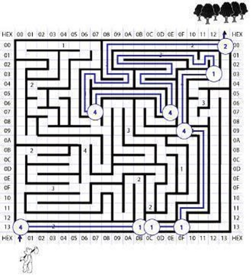
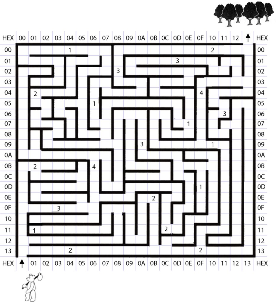
The problem we will be trying to solve for the semester was originally taken from a puzzle book. Here is the problem as defined by the puzzle book.
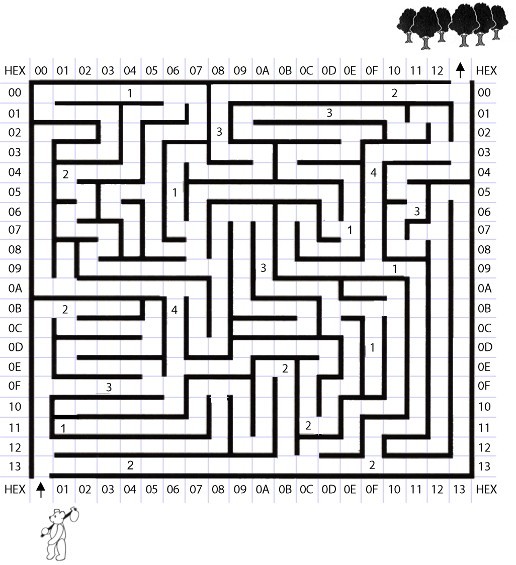
“In the forest, you will find beehives and more importantly honeycombs. Along the path are bees. The number of bees at any given location is indicated by a number. There are a few ways your bear can travel to the forest. Your aim is to teach your bear how to make his way to the forest while encountering as few bees as possible.”
Take a few minutes and see if you can solve the puzzle. While the problem may seem trivial, we will be using this as an example to show how various programming methods can be used to develop a solution that can be implemented with the assembly language that you learned in lecture. Hopefully, later on in your engineering careers, this sequence of labs will help you realize how there are many ways to resolve a problem and that creating a program may simplify the solution.
Draw a Flowchart
Now let’s see if you can translate your path through the maze into a flowchart. We will need to break it down into the individual actions that the bear can take and make sure that it can be executed by the program. This leads to the following assumptions.
- Assume the hungry Bear is initially facing north with his knapsack. In the knapsack is a blank notepad with a pencil and eraser. (This is our explanation for how the bear keeps track of various values) The length of each step is exactly one square.
- There are certain things that the bear can do or check in the attempt to exit the maze. The bear could take a step into the next room, check to see what type of room is encountered, or decide on which way to go next.
The entire list of instructions that the bear can take are listed below. Compare it with your own list of instructions that you thought to see how close you were.
Actuators and corresponding unconditional instructions
- Take a step
- Turn left
- Turn right
- Turn around
- Count and record the number of bees in your notepad
Sensors and corresponding conditional instructions
- Did you hit a wall?
- Can your left paw touch a wall?
- Can your right paw touch a wall?
- Are you in the forest?
- Do you see any bees?
- Are you thinking of a number {not equal, less than, greater than, or equal} to 0?
- Is the number on page N of the notepad {not equal, less than, greater than, or equal} to some constant?
Notepad operations
The bear can remember 8-bit unsigned and 1-bit (binary) numbers. The bear records a number in his notepad. He can only save one number per page. You may assign a descriptive name to a page (ex. bees), simply use the page number (page1), or think of it as a variable (X). In the following example X = 0.
| Pseudocode | C++ Equivalent Instructions |
|---|---|
| 1. Erase page X. | page0 = 0; |
| 2. Increment the number on a page. | page0++; |
Nodes
- Start
- Stop
Tips and Tricks
- You may not need all the instructions provided.
- Although not required, you can use subroutines.
Take a few minutes to see if you can sketch-out your flowchart. If you don’t know where to start; don’t worry, in the next few sections I will step you through how to write your own flowchart.
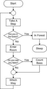
The path through the maze can be modeled as follows. Figure 2 provides an overview of the process we will be implementing in our labs. Each block can be considered a collection of the various actions described above and will be expanded on in future labs to describe exactly what our assembly program will be doing. For example, this pre-lab will focus on defining the “Which Way” block, which determines the direction the bear should face while going through the maze.
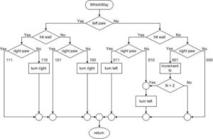
Creating the Which Way Flowchart
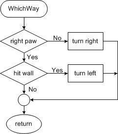
First, we need to clarify what the WhichWay block will be doing. From Figure 2, we know that the bear has just entered a room in the maze and now needs to determine which direction to go. The bear will be taking another step after the Which Way block, so we only need to make sure that the bear is in the correct orientation. There are two ways the bear can decide which way to turn when entering a room. You can count how many rooms the bear has passed or identify what type of room the bear is in. We will be doing the latter for our lab. Based on this information, these are the only instructions needed for this flowchart.
- Turn left
- Turn right
- Turn around
- Did you hit a wall?
- Can your left paw touch a wall?
- Can your right paw touch a wall?
- Increment the number on a page
- Is the number on page N of the notepad {not equal, less than, greater than, or equal} to some constant?
With that in mind, we need to define a way to identify the rooms the bear enters.
Square Naming Convention
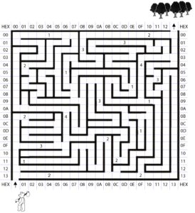
Here is a standardized naming convention to help you define the decision points in any maze. In order to provide a design example, the following maze identifies the squares (i.e., intersections) where the bear needs to make a decision for the shortest path solution.
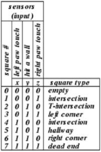
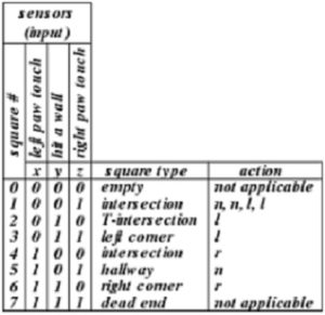
Squares are numbered by concatenating the binary values (yes = 1, no = 0) for the answers to the following three questions (sensor inputs).
Can your left paw touch a wall? – Did you hit a wall? – Can your right paw touch a wall?
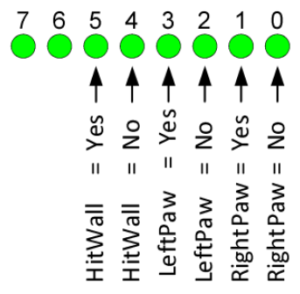
The answers to these three questions provide all the information that our bear can know about any given square. Let’s look at a few examples to see how this works. After taking the first step the bear can touch a wall with his left paw (1), has not hit a wall (0), and cannot touch a wall with its right paw (0). For our convention, this would correspond to input condition 4 = 1002. As seen in the illustration, those types of squares are labeled number 4. Assuming the bear turns right; after taking another step the bear finds himself in a hallway where his left and right paws touch a wall and he does not hit a wall. This corresponds to square 5 (1012). Although you could write a 5 in this square, for the sake of brevity, the square is left blank (your bear walks down a lot of hallways). Notice that the numbers are based on the direction the bear is facing and not a universal reference point, like facing north. This corresponds to the fact that within the maze our bear has no idea where north, or any direction for that matter, is (our bear forgot his compass). So, let’s continue to the next intersection. Here the bear’s left paw cannot touch a wall (0), he does not hit a wall (0), and his right paw can touch a wall (1). We therefore would write a 1 (0012) in this square. Continuing in this fashion all intersections are identified for our minimum solution.
Shortest Path Solution
Using the naming convention and the shortest path through the maze presented in the last section, let’s design a solution for the shortest path.
Build a Truth Table
Here are all the possible squares our bear could encounter and a short description of the situation he is facing.
For your minimum solution your bear should encounter squares 1, 3, 4, 5, and 6. Once again we did not include in our illustration situations where the bear has no choice (3 = left corner, 6 = right corner, and 5 = hallway).
Draw your Flowchart – Solution for a Fully “Deterministic” Maze
A fully deterministic maze is one where for any given intersection the bear will always (it is predetermined) take the same action. For example, for your puzzle solution, whenever the bear encounters intersection 4 he will always turn right. Fora a non-deterministic maze he may turn right one time and turn left another. If you look at our shortest solution to the maze you will discover that it is fully deterministic, and so it lends itself to this simple solution.
It is always a good idea to check your answer (or the given one) to see if it actually teaches the bear how to count bees and find the shortest path out of the maze. Once you have your flowchart, implementation in the C programming language or Assembly is fairly straightforward.
Pre-Lab Assignment
In subsequent labs, we will be working with the same bear in the same maze; however you will all be mapping out and trying to teach your bear how to follow a different path. To help everyone plot a unique path, you will need to locate your target square.
Please use the maze included at the start of this lab and “theMaze.bmp” that is linked in the Page 2 section under Deliverable for Prelab 1.
Find Your Target Square
Write down the last four digits of your student ID as two 2-digit decimal numbers. These digits will provide the coordinates (row and column) of your target square. For example, if the last four digits of your student ID were 7386, your two 2-digit numbers would be 73 and 86. Divide by 20 using long division on each number and write the remainder down. Those remainders are now your row and column numbers. In our example, 20 dives into 73 three times with a remainder of 13 and into 86 four times with a remainder of 6. Next convert both numbers into a hexadecimal number. For our example, 13 = 0x0D (where the prefix 0x signifies a number in hexadecimal) and 6 = 0x06. Your target square would therefore be in row 0x0D and column 0x06.
How to Find Your Path
Find a path through the maze such that:
- The bear goes through the target square.
- The bear must get lost at least once. Specifically, he must at some point turn-around. This is typically, but does not need to be, at a dead end.
- There are any number of paths that can take your bear through the target square, get lost, and into the forest, you now want to find the one that results in the numbers of bees encountered being closest to but not exceeding 15 (inclusive).
- Finally, the maze must be non-deterministic. This means that at some intersection along the path the bear will need to take a different action. For example, the first time he encounters a T-intersection he turns left and the second time he turns right. The good news is that, if your path meets the first three criteria, the odds are extremely high that it will be non-deterministic.
Let’s look at how you can develop a flowchart for your unique path.
Design Methodology for a Non-deterministic Maze
As previously mentioned, most maze solutions are non-deterministic. The phrase “not fully deterministic” means, while one set of input conditions in one part of the maze will determine one action (go straight), in another part of the maze the exact same conditions will require a different action (turn right). By looking at your truth-table you can recognize a “non-deterministic” path as having two or more 1’s in the same row. A quick inspection of my truth table reveals that, for the shortest path solution (Figure 4), the bear follows a fully deterministic path. Specifically, for any given intersection the bear will always take the same action. For example, if the bear’s left paw is touching a wall (1), he does not hit a wall (0), and his right right paw is not touching a wall (0), then the bear will always turn right. Following is one path example that illustrates how to solve a non-deterministic maze.
Let’s begin by looking at the sequential actions that must be taken as we encounter each intersection.
The good news is that with the exception of square number 1 all other actions are deterministic. The bad news is that only when we encounter room 1 after the second time do we start turning left. To solve this more difficult problem, we will create a binary tree that allows us to resolve all 8 squares, allowing us to then take any action needed. This binary tree can now be easily translated into C++ or Assembly.
A Modular Solution
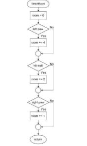
A more modular solution separates the identification of the square (referred to as a room) from the action to be taken. Identification of the room is placed into a C++ or Assembly subroutine which returns the room number. The calling program must then determine the action to be taken based on the room number returned. The flowchart for the room subroutine is provided here and once again easily implemented in C++ using if or switch conditional instructions as discussed in the next lab.
Step-by-Step Instructions
Here are step-by-step instructions for solving your maze.
Begin by making a copy (electronic or paper) of the maze and drawing your bear’s path through the maze. When you are happy with your new path, follow the methodology previously discussed to build your truth table. Verify that your path meets the design criteria (passes through the target square while encountering the minimum number of bees and getting lost once). Remember, your target square may not be along the original solution path.
It is now time to teach your bear how to navigate the new path by writing a flow chart. To accomplish your goal you will need to apply everything you have learned so far plus add a few Notepad operations. The notepad pages (i.e., variables) are used to determine which path your bear should take when he enters an intersection in which more than one action is possible. For example, the first time he enters intersection 1 you may want the bear to go straight, while the second time he encounters intersection 1 you want him to turn left. To resolve this conflict you would record in your notepad how many times intersections 1 had been encountered and then check your notepad before taking any action.
In addition to previously stated conditions, your solution must also meet the following negative criteria.
- Your solution may not use a variable (notepad) to simply count how many steps the bear has taken in order to make a decision.
- Your solution should use a variable(s) and not the number of bees encountered to help it make a decision.
Deliverable for Pre-Lab 1
Turn in the following material on the following pages (i.e., no more, no less). All work must be typed or neatly done in ink.
All labs should represent your own work – DO NOT COPY.
Title Page (Page 0)
The title page (Page 0) includes your picture (one that will allow me to match a name with a face), the lab number, your name, today’s date, and the day your lab meets.
Page 1
At the top of the page provide the last four digits of your student ID and describe how you calculated your target square. Include in your discussion how the resulting path met the design requirements defined in the pre-lab. For example how many paths did you consider before choosing your final path – how close did you come to 15.
Page 2
Next, using your favorite illustration (Visio, Illustrator, or Photoshop) program or the drawing tools included with your favorite Office program (PowerPoint, Excel, and Word) mark your target square with an X and illustrate your bear’s path through the maze). Also include on this page a table of “Sensor input combinations and actions” similar to Table 2. If you do not have access to any of those programs, there is a free online website called draw.io that works just fine.
Many drawing programs allow you to import a bitmap file, in this case the maze. You can find a bitmap and vector formatted picture of the Maze here. Once imported, draw your path, typically using the line tool. Next, number your intersections (but not corners or hallways) as illustrated in Figure 5 “Nondeterministic path example.”
Page 3
Again using your favorite drawing program, draw the flowchart for programming problem.
Your flowchart should resemble the one included with the lab and only use the provided instructions. Artwork of the sample flowchart is included here.
Page 4
Answer the following questions and complete the following table of binary, decimal, and hexadecimal numbers. You must show your work:
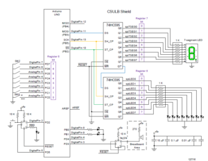
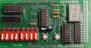
Shown below is a diagram of the CSULB Shield that you will be working with in the labs. As the semester goes on, you will be learning more about the different parts and how they interact with each other. For now, we will be focusing on the eight switches, the 7 segment display, and the eight discrete LEDs that are used in Lab 1.
Each of the switches is connected to an input pin of the Arduino Uno and the state of the switch (on or off) is represented by a value of 0 or 1. Those values are placed into register r6 by the code we will be suing in Lab 1. This way, we could figure out the state of the switches by looking at the values that are in r6. For example, if switch 7 was on, but 7 of r6 would have a value of 1.
The goal of Lab 1 is to connect the eight switches with both the 7 segment display and the eight discrete LEDs. This means that the values that are in r6 will also be copied or transferred to registers r7 and r8 respectively. If a value of 1 is copied over, that corresponding segment or LED will turn on. Answer the following questions using that knowledge.
Question 1: If switches 3 (SW.3) and 1 (SW.1) were moved to the ON position (value of 1 in r6), which segments on the 7 segment display will light up?
Question 2: Which switches need to be turned ON in order to display the number 2 on the seven segment display? Do not include the decimal point segment in your answer.
Checklist
- Your pre-lab report includes a title page (Page 0) with your picture (one that will allow the professor to match a name with a face). Title information includes lab number, your name, today’s date, and the day your lab meets (Monday or Tuesday)
- Pages are in the order specified (see Deliverable)
- You do not have any extra pages
- You describe how you arrived at your path
- Maze is not copied from another student (zero points)
- Path is computer drawn.
- Maze Path meets specified requirements
- Intersections ar not drawn by hand and appear as shown in the example
- Intersections are numbered
- Intersections are numbered correctly
- Truth table
- Truth table is on the same page as the maze
- Truth table is typed
- Truth table matches the maze
- Flowchart
- Flowchart matches your truth table
- Flowchart is correct
- Questions are answered with all work shown
Lab 1: An Introduction to Assembly
This lab is designed to introduce you to the Arduino Microcontroller Board, Atmel (part of MicroChip) Integrated Development Environment (IDE) and AVR Assembly Language programming. Plus, you will learn about the power of library files. Library files are simply files that you instruct AVR Studio to include in your program. In this lab you are going to include two library files. One named m328pdef and the other spi_shield.
Note: Please do the step-by-step simulation tutorial at the end of this lab. At the end of this tutorial you should be able to set switches to a given value by toggling Ports D and C pins. For example, after the tutorial you should be able to show how you would simulate an input of 0xAA.
Table of Contents
What is New?
The following instructions and assembly directives are used in Labs 1. If you have any questions on any instructions or assembly directives a nice source of information, in addition to your textbook, is the Atmel AVR Assembler User Guide
AVR Assembly Instructions
Data Transfer
in r6, PINC // Input port C pins (0x09) into register R6
out PORTB, r7 // Output to Port B from register R7
mov r8, r7 // Move data from register R7 into register R8
Arithmetic and Logic
clr r16 // Clear register R16
ser r17 // Set register R17
Control Transfer
call WriteDisplay //Subroutine Call
rjmp loop // Jump to the label named loop
AVR Studio Assembly
Directives
.INCLUDE // < > means the file is in the AVR Studio folder
.INCLUDE “spi_shield.inc” //” ” means the file is in the project folder
.CSEG // Code Segment
.ORG 0x0000 // Code Origin
Labels
loop:
Comments
; // /* */
Introduction to AVR Studio
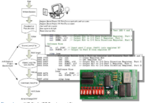
In lab you will be spending most of your time working within an IDE. For our labs we will be working in the AVR Studio IDE. As shown in the figure and discussed in the next few sections the IDE lets us write our program in a human readable form, known as assembly, and then translate it into a machine readable form understood by the ATmega328P.
Create a New Project
The best way to learn about the AVR Studio IDE is to start playing with it. So let’s get things started by launching AVR Studio and Opening a New Project.
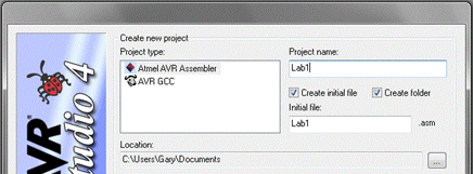
Select Atmel AVR Assembler and check both check boxes(Create initial file and Create folder). Name your project (Lab1) and browse to location where you want it saved. Click Next >>.
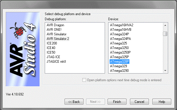
In the next window select AVR Simulator 2. For the Device, select ATmega328P. Click the Finish button.
Congratulations, you are ready to start programming within the AVR Studio IDE!
Assembly Directives
All assembly programs contain assembly directives and assembly instructions. Assembly directives are instructions to be read by the assembler. In our lab, the assembler is included with AVR Studio IDE. As you have seen, AVR Studio is a program that runs on your computer and is responsible for translating your human readable assembly program into the machine language of the microcontroller.
We begin our program with an Assembly Directive. First, locate the program window within the IDE. This is the blank window in the center of your AVR Studio application. The title bar should include the location of your program and end with the name of your program and the “.asm” extension. Enter the following lines into the program window.
You can probably guess that here we are telling the assembler that we would simply like to include some comments for the individual reading our code. To include comments, you can use the C language notation // comment line and /* block comment */ or unique to assembly a semicolon ; character.
Now let’s add some code which intended strictly for the assembler, not the reader or the microcontroller. The difference is important.
.INCLUDE.CSEG .ORG 0x0000
The “dots” tell the assembler that these lines are talking to the assembler and not to be turned into machine instructions.
Without overly complicating our first program, I will just note that the INCLUDE assembly directive tells the assembler to copy into our program all the text contained in a file named m328pdef.inc. For now, we do not need to know what is in this file, other than to note it will help us in writing a more human readable program.
The CSEG statement tells the AVR Studio Assembler to place the following material in the Code SEGment of memory. For the ATmega328P, this means Flash Program Memory. The ORG statement tells the assembler to start placing code at this address in Flash Program memory.
Programming Convention Because it is so important to remember when a line is intended for the Assembler (Assembly Directive) and when a line is to be converted to a machine instruction intended for ATMega328P microcontroller (Assembly Instruction), I always capitalize Assembly Directives and place in lower case letters Assembly Instructions. AVR Studio is not case sensitive, so this convention is not required for your assembly program to assemble correctly – it is however required by the instructor.
Now let’s add our first label. Enter the following line after the .ORG 0x0000 assembly directive:
RST_VECT:
The label RST_VECT stands for ReSeT VECTor and is only there as a point of programming style (i.e., it helps the reader know that the code to be executed on reset follows). What the assembler does is quite a different story. Whenever the assembly sees a label, it places the label name and its corresponding address, in this case we know it is 0x0000, into a look-up table.
| Label Name | Program Address |
|---|---|
| RST_VECT | 0x0000 |
Now if you ever want to reference this location in your program, you can use the name and let the assembler worry about the address.
Congratulations, you have for now completed your initial conversation with the assembler. You have asked it to include some comments, include more assembly directives located in another file, setup to write some code at address at 0x0000 in program memory, and finally to associate this address with the name RST_VECT. What you haven’t done is write anything that the AVR microcontroller will ever read. Once again it is important to know when you are talking to the assembler and when your code will be used to generate machine instructions to be run by the microcontroller. So let’s start generating assembly instructions intended for the microcontroller.
Assembly Instructions
Just as you are reading the step-by-step instructions on this page so you can write your first program, the microcontroller in Figure 5 reads the step-by-step instructions contained in the program to learn what is intended by the programmer. This is the “Machine Language” of the computer. This language is comprised of only ones and zeros. For example, this binary sequence 0010011100000000 tells the AVR computer (aka microcontroller) to set all the bits in register 16 to zero. All these 0’s and 1’s are not very easy for us humans to understand. So instead we humans have created a human like language comprised of abbreviations (known as mnemonics). This is known as Assembly Language. By definition then, there is a one-to-one correspondence between a machine instruction and an assembly instruction. For our machine code example, the equivalent assembly instruction is clr r16.
Registers Our microcontroller contains 32 general purpose registers labeled R0 to R31. For now you can think of registers like variables which can hold up to 8-bits of information (000000002 = 010 to 111111112 = 25510). To learn more about number system read Chapter 1 “Introduction” in your textbook or Appendix A – Number Systems in my Lecture 1 notes.
It is finally time to write our first assembly instruction. Add the following assembly instructions to your program.
rjmp reset // jump over the IVT, tables and include file(s)
The assembly instruction rjmp Reset instructs the microcontroller to jump to the yet to be defined label named Reset. You will also see I have included a comment. The meaning of this comment will become more clear over the remainder of the semester.
The Anatomy of an Assembly Instruction
Each assembly instruction is defined by an operator and one or two operand fields. For our clr r16 example, the clear instruction’s operator is clr and it has one operand r16. Our first program line also contains a single operand instruction. In this case, the operator is rjmp and the operand is reset.
Introduction to the Arduino Proto-shield
A schematic of our Arduino Proto-shield is shown in Figure 6. It includes 8 switches, 1 push button, 10 discrete LEDs, 1 seven segment display, and 2 D flip-flops. If you were to add up all the inputs and outputs required to support this proto-shield you would come up with 29. The Arduino Uno board, designed with the ATmega328P microcontroller, only has 23 general purpose digital I/O pins. So how do we solve the problem? Luck for us the ATmega328P includes a Serial Peripheral Interface (SPI) subsystem which allows us to send 8-bits of data as a serial string of 1’s and 0’s. By adding two 74HC595 8-bit Serial-to-Parallel shift registers to our Proto-shield as shown in Figure 6, and using the SPI subsystem, we are able to generate 16 new outputs. We will use these outputs to drive 8 discrete LEDs and our 7-segment display.
The ATmega328P Serial Peripheral Interface
Additional information can be found in Chapter 10 of the textbook or Section 18.2 of the ATmega328 Datasheet.
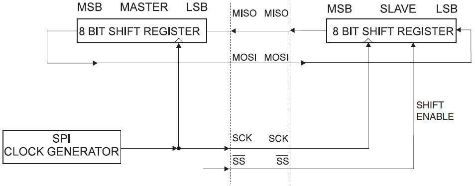
A conceptual representation of how the ATmega SPI subsystem works with our Arduino Proto-shield is shown in Figure 7 “SPI Master-slave Interconnection.” You can find the original of this picture in Section 18 “SPI – Serial Peripheral Interface” in the ATMEL doc8161.pdf document. On the left is the SPI subsystem, it includes the 8-bit Shift Register and the SPI Clock Generator. To send 8 bits of data to the Arduino proto-shield you simply need to write to this register. The SPI subsystem takes care of the reset including generating the serial data stream and clock signal. On the right is an 8-bit shift register used to convert the serial data stream back to 8 discrete bits of data. For our proto-shield this 8-bit shift register is physically realized as a single 74HC595 Serial-to-Parallel shift register. Two generate the 16 output bits used on the proto-shield we daisy chain two 74HC595s and write to the SPI’s 8-bit shift register twice.
The SPI_Shield.inc Include File
To simplify your life – it is after all the first lab – I have already written all the assembly code you need to work with the Proto-shield. This code is contained in a separate file named spi_shield.inc. We will add this file to our program in the same way we included the m328pdef.inc “include” document an earlier part of this lab. Let’s begin.
- Download and add to your Lab1 project folder my spi_shield.inc file.
- Unlike, the m328pdef.inc file which contains equate statements, the spi_shield.inc file includes subroutines which need to be run by the microcontroller.
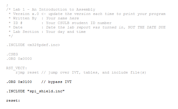
- Add the following lines of code to your Lab1 project file. Original code that you should have already added is shown in gray.
 Quick Review and New Instructions for the Assembler
- Can you Identify the comments?
- Can you tell which lines contain Assembly Directives and which contain Assembly Instructions? Remember assembly directives typically, but not always start with a period and use upper case letters; while assembly instructions use lower case letters.
Do you remember the first INCLUDE assembly directive from earlier in the lab? The m328pdef.inc library is written by Atmel and allows you to use names in place of numbers. For example PINC which was introduced in lab 1 is equated to the number 0x06 in the library. Here is the actual equate statement from the library.
.EQU PINC = 0x06
So when you press the reset button, the AVR processor will first run the rjmp reset instruction. The rjmp instruction tells the processor to jump to the code starting at the reset label. This means the program will jump over (bypass) a table known as the IVT (to be covered later in the semester) and all the code included in spi_shield.inc. Which is a good thing; because we do not want to run any of the included programs until we are ready.
I wrote the spi_shield library. This library includes subroutines InitShield, ReadSwitches, WriteDisplay which allow you to work with the Arduino Proto-shield without knowing the details of how it works.
Why are the two include files placed at different locations in the program?
The m328pdef.inc library is written by Atmel and allows us to use mnemonics (abbreviations like PINC) in place of numbers (like hexadecimal 6). To allow us to use these mnemonic names as quickly as possible we insert this library at the beginning of the program. The spi_shield library is written by the instructor and contains instructions. This code must not be executed at reset so the library is inserted after the first jump instruction (rjmp reset) and above the label reset.
If you have played around with the Arduino IDE, you know that all Arduino programs have an initialization section named setup() and a looping section named loop(). Our assembly program written within the AVR Studio IDE will be configured in a similar fashion. In our case, the initialization section is labeled reset: and the looping section is again named loop:. In the next section you will write the initialization section to be used throughout the semester.
Initialization Section
How to Initialize the Stack
To accomplish almost anything useful in assembly you write a subroutine. To allow us to work with the Proto-shield I have written a number of ready-made subroutines for you to use. When you call a subroutine you need to save your current location on a stack. All computers have built-in hardware stack support. However, before we can save our return address on the stack we need to initialize our stack pointer (SP) register. You will learn more about stacks as the semester progresses. Add the following lines of code to your program right after the reset label.
ldi    r16,high(RAMEND)    // SP = 0x08FF
out    SPH,r16
ldi    r16,low(RAMEND)
out    SPL,r16
How to Use the InitShield Subroutine
We are now ready to call our first subroutine. Add the following line to your program.
call InitShield
The InitShield subroutine takes care of all the initialization required to use the Arduino Proto-shield. You only need to call it once at the beginning of your program, just after stack initialization. That is it, you are now ready to use the ATmega328 GPIO Ports and SPI subsystem to work the Arduino Proto-shield – allowing you to read the 8 switches and whenever you want to update the 7 segment display and/or 8 discrete LEDs. To make your life even simpler the spi_shield file also includes the subroutines ReadSwitches and WriteDisplay.
Looping Section
To programmatically connect our switches to the 7 Segment display we will (1) read the 8 switches into register r6, (2) move register r6 into r7, and (3) then write r7 to the 7 Segment display. We will maintain the connection by looping the program around these three instructions using the Relative Jump (rjmp) instruction. To accomplish steps 1 and 3 you will use two subroutines that I have already written for you named ReadSwitches and WriteDisplay. In the next two sections we will take a closer look at both.
You can find out more about these and other instructions in AVR Studio by clicking Help in the menu bar and selecting Assembler Help. Let’s take a little closer look at our program and how it works.
How to Use the ReadSwitches Subroutine
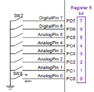
In Figure 6, on the left hand side, you see bits in Register 6 (in purple) assigned to each of the 8 switches. Register 6 is not hardwired to the switches. Instead, we will use the ReadSwitches subroutine to read the GPIO ports and perform all the logical operations needed to map these switches to Register 6.
Remember, changing the switches does not automatically change the value in register r6 – you must call ReadSwitches.
How to Use the WriteDisplay Subroutine
In Figure 6, on the right hand side, you see bits in Register 7 and Register 8 (in purple) assigned to each of the lines controlling the input pins of the 7 segment display and 8 discrete LEDs. To change the 7 segment display or any one of the discrete LEDs, you make the change to bit(s) within the associated register and call the WriteDisplay subroutine. The WriteDisplay subroutine will take care of all of the housekeeping required to map these bits within the registers to their corresponding pins. Please, do not get confused. These registers are not hardwired to the 7 segment display and discrete LEDs. Instead they are used as arguments to the WriteDisplay subroutine which sends them to the SPI Serial Register, which in turn sends them as a serial stream of data to the 74HC595 ICs on the Arduino Proto-shield (see Figure 7).
If you are asking yourself “What is a 7 segment display?” and “What is a 74HC595?” among probably many other questions, you can find many of your questions answered in Appendix B “How the Parts of the Arduino Proto-Shield Work.”
Remember, changing bits within these registers does not automatically change the pins on the 7 segment display or discrete LEDs – you must call WriteDisplay.
In the next section we will see how the ReadSwitches and WriteDisplay subroutines can be used to create software wires between the 8 switches and 7 Segment display.
Making SPI Software Wires
Because the switches are not physically connected to the 7 segment display, we must create software wires to transfer the data. In this section, we want to connect all 8 switches to their corresponding segments of the 7 Segment display (the numeric display on the top right in Figure 8) using our two new subroutines and a new assembly instruction. Once you have completed this section, the CSULB shield should work as discussed in the questions from Prelab 1.
Let’s review what you have accomplished to date. In “The SPI_Shield.inc Include File” section you initialized the stack pointer and included SPI subroutines InitShield, ReadSwitches, and WriteDisplay. You ended by calling InitShield to setup the SPI Subsystem of the ATmega328P microcontroller.
In the “How to Use the ReadSwitches Subroutine” section you learned how to connect the 8 switches on the Proto-board to Register 6 (in purple) as illustrated on the left hand side of Figure 8. In the “How to Use the WriteDisplay Subroutine” section you learned how Register 7 and Register 8 (in purple) can control the input pins of the 7 segment display and 8 discrete LEDs. To make our software wires we simply need to move the contents of Register 6 into Register 7. To do that, we will use the assembly mov instruction. Add the following lines to your program.
The rjmp instruction loops back so that future changes made to the switches are sent to the 7 segment display.
On Your Own
Apply what you have learned by connecting the 8 switches to the eight discrete LEDs. Add the appropriate instruction to do this to the main loop. Like the 7 segment display which is mapped to register r7, the eight discrete LEDs are mapped to register r8. Your code should now update both the 8 discrete LEDs and 7 segment display. You only need to call the WriteDisplay subroutine once.
Debug Workshop 1 — Simulate Your Program
Important The following section summarizes what you learned in Debug Workshop 1 covered in Lab 1 Part A and introduces the step over button ![]() to skip over subroutine calls. You must complete this section before starting lab 2. You may/will be tested (ex. Quiz 1) on the information contained in both Debug Workshops (1 and 2) plus you will need to demonstrate proficiency with the simulator (i.e., debugger) as part of the sign-off for lab 1.
to skip over subroutine calls. You must complete this section before starting lab 2. You may/will be tested (ex. Quiz 1) on the information contained in both Debug Workshops (1 and 2) plus you will need to demonstrate proficiency with the simulator (i.e., debugger) as part of the sign-off for lab 1.
PLEASE REFER TO THE SIMULATION TUTORIAL FOR ADDITIONAL INFORMATION AND TO UNDERSTAND WHAT YOU ARE DOING.
Assemble your program by pressing the Assemble F7 ![]() icon. If there are no syntax errors you should see the following line in the Build window pane (usually located at the bottom of the screen).
icon. If there are no syntax errors you should see the following line in the Build window pane (usually located at the bottom of the screen).
Assembly complete, 0 errors. 0 warnings
Important – Reading and Remembering can SAVE HOURS OF TIME!
- One very common misconception is that when the assembler says there are 0 errors and 0 warnings that your program will work. That is almost always not the case! This message only tells you that the assembler understood everything you entered. Technically speaking, it is saying that your syntax is correct. Unfortunately, ninety-nine times out of a hundred your program still contains “programming” or logical errors. You have to find these errors all by yourself. Luckily, AVR Studio includes a Simulator to help you.
- Students try to make their broken programs work by making random changes and downloading them to their Arduino boards to see if they “now” work. This process is repeated for hours upon hours until more errors are introduced than corrected. I typically receive an email after 4 to 8 hours of frustration, asking why the program doesn’t work. The first thing I ask is if they have simulated the program. The typical answer is NO. One of the reasons I am including this lab at this early stage in the course, is so you cannot download to your Arduino board and so make this common mistake. ALWAYS SIMULATE YOUR PROGRAM.
Once your program has assembled successfully enter AVR Studio’s debug mode by pressing the Assemble and Run ![]() icon.
icon.
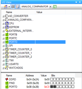
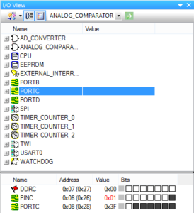
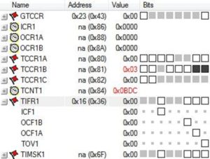
If closed, expand the Registers folder in the Processor pane and PORTC and PORTD in the I/O View pane within AVR Studio. Select PORTD. In the window below the I/O View, you will notice that PORTD has three rows of eight bits, represented by square boxes.
Each box corresponds to a flip-flop or pin as defined in Table 1 “Port Pin Configurations.”
| Inputs | Outputs | |||
|---|---|---|---|---|
| DDRXn | PORTXn | I/O | Pull-up | Comments |
| 0 | 0 | Input | No | Read “Synchronized” PINXn |
| 0 | 1 | Input | Yes | |
| 1 | X | Output | N/A | Write bit to PORTXn |
Looking at Figure 9, lets start with the first row and the Port D Data Direction Register (DDRD). Each box in this row corresponds to flip-flop. As defined in Table 1, if this box is filled in (Flip-Flop DDRXn = 1) then this port pin will be an output. Conversely, if the box is not selected then the port pin will be an input.
The second row of Figure 9 may be visualized as a physical Port D pin (PIND). If you want to simulate a change on an input pin, say from a switch being toggled, this is the box you would set (input = 1) or clear (input = 0).
The third row contains the Port D register (PORTD). Each box in this row corresponds to flip-flop PORTxn. As described in Table 1, these flip-flops are interpreted differently based on if the port pin is defined as an input (DDRXn = 0) or an output (DDRXn = 1). If DDRXn = 0 (input), then the corresponding PORTXn flip-flop adds (PORTXn = 1) or removes (PORTXn = 0) a Pull-up resistor (see fourth column in Table 1). If DDRXn = 1 (output), then the corresponding PORTXn flip-flop defines the output state of the pin. For example, if PORTXn = 1, the pin is driven high. If you want to see how your program modifies a pin defined as an output, PORTXn is the box you would look at.
As an example, lets assume all Port D pins are to be inputs with pull-up resistors assigned to the two most significant inputs. In this case all the boxes in the DDRD (second row) would be empty (logic 0) and the two most significant boxes of the last row would be filled in (logic 1). This is the case depicted in Figure 9.
The above example corresponds to switches 7 and 6. To simulate turning a switch ON simply check the box corresponding to the desired input pin (PIND).
By clicking on the Step Over (F10) ![]() button, single step the program to the last line of your program.
button, single step the program to the last line of your program.
Now, open the PORTC window by selecting PORTC in the I/O View window.
Let’s simulate switch SW0 in the up/ON position (logic 1) by checking the first box in the PINC Register.
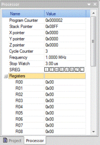
With respect to Table 1 “Port Pin Configurations” and the above image (Figure 10), note that PORT C bit 0 has been configured as an input with a pull-up resistor and the input is currently at logic 1. If it is not already open, expand the Register entry in the Processor window pane (normally located in the upper-left window pane). Notice that register R06 is cleared (0x00)
Single step (using Step Over) through your program so the input instruction is executed:
call ReadSwitches // read switches into r6
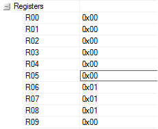
In the Processor window you should now see r06 now set to 1 (0x01).
Single step your program so the output instruction is executed:
call WriteDisplay // write r7 to the 7 segment display
If you have followed the lab instructions exactly and correctly written your one line of code, you should now see the following in the processor window:
Lab Sign-off
At signoff, you will be given an arbitrary hexadecimal number. You should be able to convert this number to binary and simulate the corresponding switch configuration using the PINC and PIND registers in AVR Studio. You should also be able to use the processor window to demonstrate that your program does, in fact, programmatically “wire” the switches to the 7-segment display (r7) and discrete LEDs (r8).
For example: given 0xA2, input 0b10100010 into PINC and PIND registers.
How to Create and Print-out a List (.lst) File
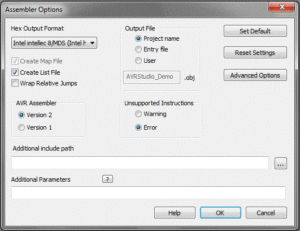
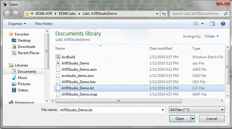
At the end of each lab, you will turn in a List file version of your program. A list file contains both your assembly program and the machine program generated by the assembler. First let’s verify that AVR Studio is set to generate a List file. In the menu bar select Project and then Assembler Options
Now whenever you assemble your program, a file with a .lst extension will be created in your project folder. Assemble your program and then open the generated list file.
You will see that along with your program the list file includes a lot of other stuff. Most of this is the text from the included m328pdef.inc document. This is the document that includes all the equate Assemble Directives which allow us to use mnemonics for all our registers in place of their actual addresses. If you have not done so already browse this material to see how AVR Studio does it. You should see something like the following.
AVRASM ver. 2.2.7 c:\users\Documents\Lab1\Lab1.asm Tue Aug 21 13:05:53 2018

[builtin](2): Including file 'C:/Program Files (x86)\Atmel\Studio\7.0\Packs\atmel\ATmega_DFP\1.2.209\avrasm\inc\m328pdef.inc'
c:\users\Documents\Lab1\Lab1.asm(10): Including file 'C:/Program Files (x86)\Atmel\Studio\7.0\Packs\atmel\ATmega_DFP\1.2.209\avrasm\inc\m328pdef.inc'
c:\users\Documents\Lab1\Lab1.asm(16): Including file 'c:\users\Documents\Lab1\spi_shield.inc'

/* Lab 1 - An Introduction to Assembly

* Version x.0 <- update the version each time to print your program
* Written By : Your name here
* ID # : Your CSULB student ID number
* Date : Date the lab report was turned in, NOT THE DATE DUE
* Lab Section : Your day and time
*/

;***** Created: 2011-02-09 12:03 ******* Source: ATmega328P.xml **********
;*************************************************************************
;* A P P L I C A T I O N N O T E F O R T H E A V R F A M I L Y
;*
;* Number : AVR000
;* File Name : "m328Pdef.inc"
;* Title : Register/Bit Definitions for the ATmega328P
;* Date : 2011-02-09
There is a lot of extra material that is not useful, so there are several things to remove. Everything that comes from any include file must be removed since it is not a part of the main code. Delete material from this line…
;***** Created: 2009-12-11 15:36 ******* Source: ATmega328P.xml **********
;*************************************************************************

up to and including this line.

; ***** END OF FILE ******************************************************
Your list file must include the AVR Studio Assembler version and time stamp!
AVRASM ver. 2.1.42 Tue Aug 23 16:57:15 2011
The “Resource Use Information” should also be deleted before you print out your list file.
Delete material from this line…
RESOURCE USE INFORMATION
------------------------
up to, but not including this line.
Assembly complete, 0 errors, 0 warnings
You can clean up and format the final version of your file in AVR Studio or your favorite text editor. Regardless of the text editor your final document should be formatted as follows.
Font: Courier or Courier New
Size: 9 or 10 point
Paragraph Spacing: 0 pt before and after
Line Spacing: Single
Page Layout: Landscape
Next, clean up unwanted spaces so your code is aligned and easy to read. DO NOT FORGET THIS STEP. Your touched up list file should now look something like this template.
AVRASM ver. 2.1.42 Tue Jan 10 11:24:47 2013 /* Lab 1 - An Introduction to Assembly * Version x.0 <- update the version each time to print your program * Written By : Your name here * ID # : Your CSULB student ID number * Date : Date the lab report was turned in, NOT THE DATE DUE * Lab Section : Your day and time */ .CSEG .INCLUDE.ORG 0x0000 RST_VECT: 000000 c131 rjmp reset // jump over IVT, tables, and include files .ORG 0x0100 // place all the code that follows starting at the address 0x0100. .INCLUDE "spi_shield.inc" reset: // Initialize the stack pointer 000132 e008 ldi r16, HIGH(RAMEND) // IO[0x3e] = 0x08 000133 bf0e out SPH, r16 000134 ef0f ldi r16, LOW(RAMEND) // IO[0x3d] = 0xFF 000135 bf0d out SPL, r16 000136 940e 0100 call InitShield loop: 000138 940e 0116 call ReadSwitches // read switches into r6 00013a 2c76 mov r7,r6 // wire switches to the 7 segment display 00013b 940e 0121 call WriteDisplay // write r7 to the 7 segment display 00013c cffb rjmp loop Assembly complete, 0 errors, 0 warnings
NOTE: THIS IS JUST AN EXAMPLE. YOUR LIST FILE SHOULD CONTAIN THE CODE FOR THE LAB YOU ARE SUBMITTING.
Finally, if you have not done so already, set your printer page layout to landscape mode. Preview your printout before you actually print it out to save paper. Double check your document to make sure there is no word wrap. Your printout should never include word-wrap. If you do see a line wrapping in the print-out, go back and correct the line and re-print your list file. Print your list file.
Now single step ![]() your program noting how the change input modify the registers. Use the step over button
your program noting how the change input modify the registers. Use the step over button ![]() to skip over the subroutine call instructions. This button tells the simulator to run the code in the subroutine without showing you.
to skip over the subroutine call instructions. This button tells the simulator to run the code in the subroutine without showing you.
Follow the instructions in Lab 1 “Debug Workshop 1” to simulate your program and verify your program reads the switches and moves them to register r7. Until you actually build your own proto-shield you will have to assume that my WriteDisplay subroutine works.
Design Challenge (2 Points)
You can skip this section if you are happy receiving a passing or even a good grade on the lab. If you want to receive an excellent grade you will need to accept the challenge. Specifically, the maximum grade you can receive on this lab if you do not accept the challenge is 18 points.
The purpose of this design challenge is to help you better understand how the I/O ports work and to how the subroutines ReadSwitches and WriteDisplay are written.
The SPI Shield which you will be assembling soon has two green status LEDs. They are connected to the two least significant bits of PORTB, as shown in Figure 15. The design challenge for Lab 1 is to create software “wires” between switches 6 and 3, connected to PIND6 and PINC3, and these two green LEDs. Make sure that switch 6 connects to PORTB1 and switch 3 goes to PORTB0.
This can be accomplished by implementing something similar to the ReadSwitches subroutine, where the inputs are read from the desired I/O port and then written to the output I/O port. Refer to Appendix A for an explanation of how the InitShield and ReadSwitches subroutines work. Note that if you are correctly calling the InitShield subroutine, you do not need to modify any of the Data Direction Registers (DDRx). PORTB should look like this if both LEDs are turned on after correct execution of this challenge:
Lab 1 Deliverable(s) / Checklist
STOP Read the Lab READ ME document contained in the Labs Folder. Be absolutely sure you have followed all instruction in the “Lab Formatting” section of this document. Points will be deducted if you do not follow these instructions. You have been warned.
If you have not done so already, please purchase a Lab Notebook. Follow the guidelines provided in the “Lab Notebook” section of the Lab READ ME document.
Make sure you have read and understand the “Plagiarism” section of the Lab READ ME document, especially if you are repeating the class.
All labs should represent your own work – DO NOT COPY.
Remember before you turn in your lab…
- Does your software program “wire” the switches to the 8 discrete LEDs and the 7 segment display?
- Your lab report includes a title page with your picture (one that will allow me to match a name with a face), lab number, your name, today’s date, and the day your lab meets
- The above information is duplicated in the title block of your assembly program as described in the lab. Do not forget to include the first line of your program containing the title of the lab. If you are not careful this line may be deleted and points deducted.
- Your list file should include the AVR Studio Assembler version and time stamp.
- Your list file should not include material from the m328pdef.inc or spi_shield libraries or Resource Use Information.
- Include the Assembly line indicating that your Assembly program contains no errors or warning in syntax.
- Your list file should be formatted as defined here.
Font: Courier or Courier New
Size: 9 to 10.5 point
Paragraph Spacing: 0 pt before and after
Line Spacing: Single - All fields within the program area (address, machine instruction, label, operand, destination operand, source operand, comment) must be aligned.
- Your list file printout should be in landscape and not have any lines wrap from one line to the next.
- Never turn in a program that is not debugged (i.e., contains logical errors).
Appendix
Appendix A: A Quick Look at SPI_Shield
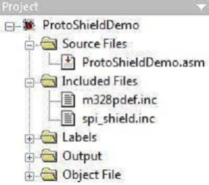
To look at the assembly code in spi_shield.inc; inside the Project window, double-click the spi.inc file in the Included Files folder. You may need to reassemble ![]() the program if the folder is empty.
the program if the folder is empty.
You should now be able to tab between the Lab2.asm (named ProtoShieldDemo in the screen capture) and spi_shield.inc files open in the Workspace window. In the Workspace window select the Lab2.asm tab to view this file.
How the InitShield Subroutine Initializes the GPIO Ports C and D
We begin by initializing PORT D bits 7 to 6 and PORT C bits 5 to 0 as inputs with pull-up resistors. To find out the correct bit settings study Table 1 “Port Pin Configurations.”
| DDRXn | PORTXn | I/O | Pull-up | Comments |
| 0 | 0 | Input | No | Read “Synchronized” PINXn |
| 0 | 1 | Input | Yes | |
| 1 | X | Output | N/A | Write bit to PORTXn |
In this lab we want to configure 8 switches so a byte wide solution makes the most since. The Set Bit(s) in Register (sbr) and Clear Bit(s) in Register (cbr) assembly instructions provide us with our 8-bit solution. The sbr and cbr work with registers, so we will have to first load the Data Direction registers (DDRC, DDRD) and PORT (PORTC, PORTD) registers into one of our 32 general purpose registers, before you can set or clear any of the bits. The sbr, cbr give us the ability to set or clear multiple bits. This is done by setting the bit you want set or cleared to 1, with 0 indicating don’t change.
Reviewing Figure 1 you will notice switches 7 and 6 are wired to Port D bits 7 and 6 and switches 5 to 0 are wired to Port C bits 5 to 0. Consequently, it is these bits within the two Ports that we want to configure as required by Table 1 “Port Pin Configurations.” Study the comments following each of the instructions below to see how this was done.
; Initialize Switches with Pull-up resistors and Test LEDs
in r16,DDRC // input Port C DDR (0x07) for switches 5 to 0
cbr r16,0b00111111 // define bits 5 to 0 as input (clear bit reg.)
out DDRC,r16 // output
in r16,PORTC // input Port C Reg. (0x08) for switches 5 to 0
sbr r16,0b00111111 // add pull-up resistors (PUR)
out PORTC,r16 // output
in r16,DDRD // input Port D DDR (0x0A) for switches 7 to 6
cbr r16,0b11000000 // define bits 7 to 6 as input (clear)
out DDRD,r16 // output
in r16,PORTD // input Port D Reg. (0x0B) for switches 7 to 6
sbr r16,0b11000000 // add pull-up resistors (PUR)
out PORTD,r16 // output
How ReadSwitches Subroutine Maps the 8 Switches to General Purpose Register 6
In this section I am going to show you how I wrote the code to wire the 8 switches to their corresponding bits in Register 6. This virtual connection of the switches to Register 6 is illustrated on the left hand side (in purple) in Figure 1.
Looking at Figure 1 you will notice that while switches 7 and 6 are wired to Port D bits 7 and 6, switches 5 to 0 are wired to Port C bits 5 to 0. Consequently, I needed to read the pins of both ports and then concatenate bits 7 and 6 of Port D with bits 5 to 0 of Port C.
loop:
; SPI Software Wires
in r17, PINC // input port C pins (0x06) into register r17
in r16, PIND // input port D pins (0x09) into register r16
Before I could concatenate (combine) the two registers I needed to clear the unused bits. The Clear Bit(s) in Register (cbr) assembly instructions works perfectly when you want to selectively clear more than one bit while not modifying other bits within the destination register.
cbr r17, 0b11000000 // clear non-switch bits 7 and 6
cbr r16, 0b00111111 // clear non-switch bits 5 to 0
The notation 0b tells the assembler that the following bits are in binary. So 0b11000000 = 110000002. I could just as easily have typed 0xC0. In this case I used binary to more easily show which bits were being cleared (a 1 is placed in the position to be cleared) and which were not being modified (a 0 is placed in the position to not be modified). Finally, I was ready to combine the bits. The logical or operator is used to accomplish this goal. Reviewing what you learned in your Digital Logic Design class.
| x | y | x OR y | |
| 0 | 0 | 0 | |
| 0 | 1 | 1 | |
| 1 | 0 | 1 | |
| 1 | 1 | 1 |
Because I had set to 0 the bits to be set or cleared by the other register, we only need to look at the first two lines in the table to see how it works. If the target bit is 0 it will remain 0 and if it is 1 it will remain 1. After we have merged our two registers we move the result into register 6 as required by Figure 1.
or r16, r17 // concatenate switches SW7 – SW6 : SW5 – SW0
mov r6, r16 // move to standardized switch register
; SPI interface registers
.DEF spiLEDS=r8
.DEF spi7SEG=r7

; Switches
.DEF switch=r6

; Temporary storage of AVR Status REGister Flag bits
.DEF reg_F=r15

; 7-segment display
.EQU seg_a=0
.EQU seg_b=1
.EQU seg_c=2
.EQU seg_d=3
.EQU seq_e=4
.EQU seg_f=5
.EQU seg_g=6
.EQU seg_dp=7

InitShield:
; Disable interrupts and configure stack pointer for 328P
cli

; Initialize Switches with Pull-up resistors and Test LEDs
in r16,DDRC        // input Port C Data Direction Register (0x07) for switches 5 to 0
cbr r16,0b00111111 // define bits 5 to 0 as input (clear bit register)
out DDRC,r16       // output

in r16,PORTC       // input Port C Register (0x08) for switches 5 to 0
sbr r16,0b00111111 // add pull-up resistors (PUR)
out PORTC,r16      // output

in r16,DDRD        // input Port D Data Direction Register (0x0A) for switches 7 to 6
cbr r16,0b11000000 // define bits 7 to 6 as input (clear)
out DDRD,r16       // output

in r16,PORTD       // input Port D Register (0x0B) for switches 7 to 6
sbr r16,0b11000000 // add pull-up resistors (PUR)
out PORTD,r16      // output

; Initialize SPI Port
in r16,DDRB        // Input from Port B Data Direction Register (DDRB) at i/o address 0x04
sbr r16,0b00101111 // Set PB5, PB3, PB2 (SCK, MOSI, SS) and PB1, PB0 (TEST LEDs) as outputs
out DDRB,r16       // Output to Port B Data Direction Register (DDRB) at i/o address 0x04

ldi r16,0b01010001 // Set SPCR Enable (SPE) bit 6, Master (MSTR) bit 4, clock rate fck/16 (SPR1 = 0,SPR0 = 1)
out SPCR,r16       // Output to SPI Control Register (SPCR) at i/o address 0x2c

cbi PORTB,2 // Clear I/O Port B bit 2 (SS) at i/o address 0x05
cbi PORTB,1 // Clear I/O Port B bit 1 (TEST LED1)
cbi PORTB,0 // Clear I/O Port B bit 0 (TEST LED0)
ret

ReadSwitches:
; SPI Software Wires
push r17
push r16

in r17, PINC // input port C pins (0x06) into register r17
in r16, PIND // input port D pins (0x09) into register r16

cbr r17, 0b11000000 // clear non-switch bits 7 and 6
cbr r16, 0b00111111 // clear non-switch bits 5 to 0

or r16, r17 // concatenate switches SW7 - SW6 : SW5 - SW0
mov r6, r16 // move to standardized switch register

pop r16
pop r17
ret

WriteDisplay:
; Save SREG
push reg_F
in reg_F, SREG
; Start transmission of data
out SPDR,spiLEDS
rcall spiTxWait
out SPDR,spi7SEG
rcall spiTxWait
sbi PORTB,PB2 // strobe latches
cbi PORTB,PB2
; Restore SREG
out SREG, reg_F
pop reg_F
ret

SpiTxWait:
push r16
; Wait for transmission complete
spiPolling:
in r16,SPSR
bst r16,SPIF
brtc spiPolling
pop r16
ret

; --------------------------
Appendix B: How the Parts of the Arduino Proto-Shield Work
This appendix was written by Bryan Everett, and is designed for the student who does not want to wait to find out how the proto-shield works. In addition to this material you may also want to read “ATmega328P Serial Communications.”
The 74HC595 Shift Register
The 74HC595 is a high speed CMOS shift register. It has one serial data input with eight (8) parallel output. In this section we will learn how each of these pins control the 74HC595 shift register and what is going on inside the “595”
Let’s discuss the components that make up the 74HC595 shift register.
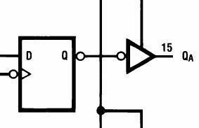
Tri-State Output Buffers
The eight parallel-out pins of this shift register are driven by tri-state buffers. A tri-state buffer is a device commonly used on shift registers, memory, and many other kinds of integrated circuits.
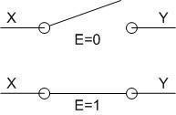
The tri-state buffer shown above has two inputs, data (X) and control (E), which control the state of the output (Y). Just as the name implies, there are three output states: high, low and high impedance. When the pin labeled “E” is high, the output is equal to the input (Y=X).
Not very interesting, right? Well, when the pin labeled “E” is low, the output is in high impedance mode. In high impedance mode, the output is virtually disconnected from the input, neither high nor low. The basic operation of a tri-state buffer can also be easily understood if compared to a switch. When the “E” pin is high, the switch is closed, and when the “E” pin is low, the switch is open. In the context of our shift register, the output pins will either contain our data or will be in high impedance mode.
For more information regarding tri-state buffers, click here.
National Semiconductor – Tri-State Buffer IC
Storage Registers (D Flip-flops)
Looking further into our shift register we see the storage registers. These registers are made up of D-type flip flops. The D-type flip flop is capable of storing one bit of memory. The D-flip flop’s function is to place on the output whatever data is on its input when the flip flop detects a rising edge signal (input buffer inverts clock before input of FF shown) on the clock port. This works by placing the data to be stored (1 or 0) on the D pin. Once the data is on the D line, the clock pin must be pulsed high. On the rising edge of the pulse the data on the D pin will appear on the Q pin.
In context to our shift register, when the data appears on D pins of the storage registers and is ready to be displayed, the clock pin is pulsed and the data is sent to the tri-state buffers.
For more information regarding D-type flip flops, click here.
Fairchild Semiconductors – D-Flip Flop
Shift Registers (D Flip-flops
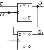
The shift registers are final stage and are made up of D-Flip flops as well. These are the heart of our 74HC595 shift register. Below is a simplified version of what makes our shift registers work. What we have there is two D-type shift registers. The output of the first D flip flop is connected to the input of the second D flip flop. The clock pins are connected together on all D flip flops.
To understand how this shift register works, we will look at a two bit shift register:
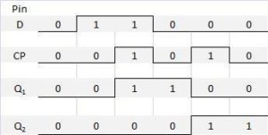
Suppose we want to set Q2 high and Q1 low:
- The D pin is set high.
- The clock pin is pulsed high once. (This makes the output Q1 high. Q1 is connected to the input of the second D flip flop)
- The D pin is brought low.
- The clock is pulsed once again.
- The result is Q1 = 0 and Q2 = 1.
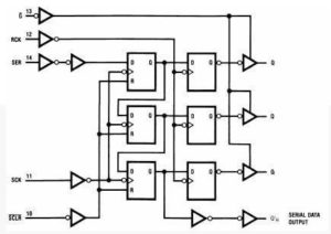
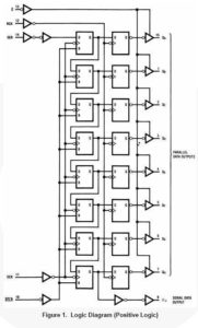
The above example only covers a two bit shift register. Below is the logic diagram of our 74HC595 8-bit shift register.
MM74HC595 Logical Diagram by Fairchild Semiconductor
Below is the timing diagram of our 74HC595 8-bit shift register.
MM74HC595 by Fairchild Semiconductors
For more information regarding shift registers, see AllAboutCircuits.com
Seven Segment Display
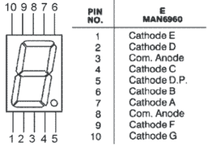
Just as you learned in EE-201, seven segment displays made up of seven (eight with a decimal point) LEDs arranged and shaped such that numbers between 0 and 9 can be displayed. There are two basic kinds of seven segment displays, common anode and common cathode. This simply means that they share either a supply or ground connection. Other than that, these seven segment displays function just as seven separate LEDs. The Arduino Proto-Shield uses a common cathode display.
Source: ElectronicsLab – Common Anode.
Each of the segments includes a 1 Kohm resistor to limit current though the LED. The resister values are calculated by: (VDD – VLED)/ILED.
Since the segments function as individual LEDs, see LED Basics for more information.
Appendix C: Reference
- Here is a New York University (NYU) lab for the 74hc595 shift register and the Arduino: http://www.makingthingsmove.org/blog/?p=248
- Serial to Parallel Shifting-Out with a 74HC595, http://www.arduino.cc/en/Tutorial/ShiftOut
- 74HC595 Data Sheet: 8-bit serial-in, serial or parallel-out shift register with output latches; 3-state multiplying arduino outputs/inputs
- Atmel ATmega328 datasheet doc2545.pdf, Section 16 SPI – Serial Peripheral Interface (pages 160 to 162)
- Atmel AVR Microcontroller Primer: Programming and Interfacing by Steven F. Barrett, Section 2.3.3 Serial Peripheral Interface (pages 34 to 39[1]
- Programming and Customizing the AVR Microcontroller by Dhananjay Gadre, Section 6.6.1 I/O Expansion using Shift Register (page 110 to 1111)
- Embedded C Programming and The Atmel AVR 2nd Edition by Richard H. Barnett, Section 2.10 Serial Communication using the SPI (page 151 to 157[2])
- University of Maryland – Tri-state Buffer
- Hobby Projects – D-type Flip Flop
[1] Assumes ATmega16
[2] Assumes ATMega16 and ATMega128
Pre-Lab 2: Room Builder and Direction Finder
Table of Contents
Introduction
The Wake-up Machine
Plus Arduino Uno Version
In this prelab you will (1) learn more about the assembler, (2) learn how a 7-segment display works, (3) apply what you learned to display rooms within the maze on the 7-segment display and finally apply what you learned in EE201 “Digital Logic Design” and CECS100 to display the direction the bear is facing using (4) Boolean Expressions and (5) A flowchart.
The Assembler
Seven Segment Display
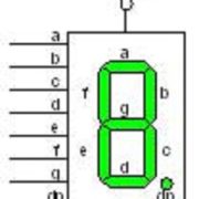
In this section, you will learn how a 7-segment display works. A 7-segment display is comprised of 7 LEDs labeled a-to-g plus the decimal point (dp).
Each LED segment can be represented as a single LED as shown schematically here with one of the in-line resistors.
When the input (anode) of the LED is connected to a 5v source through a limiting resistor and the output (cathode) is connected to ground, the LED is said to be forward biased. The LED emits light when operating in this mode (ON). If instead we wire the anode of the LED to ground, then no current can flow in the circuit and the LED is said to be reverse biased (OFF).
Traditionally, a 7-segment display is used to form all 10 digits (0-9) by turning on or off the LEDs in different combinations. For example to create the number 1 you would turn on segments b and c.
Part A – Room Builder
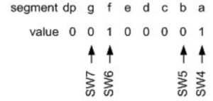
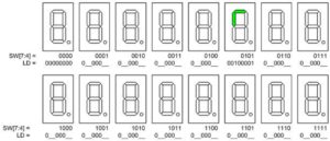
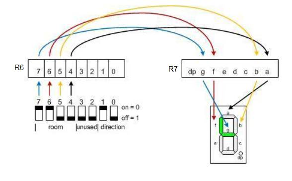
In the first half of the lab, instead of numbers we will be using our 4 switches and the 7-segment display to draw the 24 = 16 different rooms that our bear may encounter in any maze. As an example, let’s use our four switches to draw a room with a north and west facing wall. For this room we would turn on (up position) switches 6 and 4, leaving switches 7 and 5 in the off position (down). The resulting room configuration is shown in Figure 2.
Here are the sixteen possible situations or “rooms” our bear may find as he explores the maze. The decimal point dp and segments c, d, and e are always “off.” Segments a, b, g, and f are turned “on” and “off” to show the room configuration. Working from Figure 2, complete the drawing below by filling in the LED pin values and coloring in the LEDs that are turned “on” for each switch SW[7:4] combination. I have included a file named Room_Combination.JPG here for you to use.
After completing the drawing above you may have noticed that the following relationships exist between our switches SW[7:4], returned in register r6 by ReadSwitches, and the 7-segment LEDs, sent in register r7 as an argument to WriteDisplay. Figures 4 “MazeRoom” graphically shows how your program will work.
In the previous lab you connected your eight (8) switches to the 7-segment display by using the mov instruction. In essence you created a “software” wire between register 6 bit 0 and register 7 bit 0, register 6 bit 1 and register 7 bit 1, etc. As seen from a quick look at the crossing lines in Figure 4, this solution will unfortunately not work for your room builder code. Instead you will use two new bit instructions. The “Bit Store from Bit in Register to T Flag in SREG” (bst Rd, b) and the Bit Load from T Flag in SREG to Bit in Register” (bld Rd, b) instructions. Here is how these two bit instructions would be used to create the blue “software wire” between register 6 bit 7 and register 7 bit 6 (seven segment display segment G).
call ReadSwitches
bst r6,7 // wire switch 7 to segment g (south wall)
bld r7,6
call WriteDisplay
As shown in Figure 4, the call to ReadSwitches places the state of the eight (8) switches on the proto-shield into register r6 and the call to WriteDisplay copies the bits in register 7 to the 74HC595 8-bit Shift Register IC wired to the 7-segment display (see proto-shield schematic). The two lines bst and bld therefore functionally wire switch 7 to segment g. Let’s take a closer look.
Turn to “Appendix C ATMEGA328P Assembly Instructions” in your textbook and specifically Table C.4: “Bit and Bit-Test Instructions” or the free 8-bit AVR Instruction Set document 0856 available from Atmel, you can find it here.
The bst “Bit Store from Register to T” instruction copies bit 7 from register 6 into the T flag bit located in the status register (SREG) of the AVR processor. You can think of T as our general purpose 1-bit register. As most 8-bit data uses one of our 32 general purpose, single bits of data use the T bit. The bld “Bit load from T to Register” completes our “software” wire by sending the contents of the T bit to register 8 bit 6.
Working from the above example you should be able to write the next six assembly instructions to wire switches 6, 5 and 4 to 7-segment LEDs f (west wall), b (east wall) and a (north wall) respectively.
call readSwitches
bst r6,7 // wire switch 7 to segment g (south wall)
bld r7,6
… your code goes here
call writeDisplay
Part B – Direction Finder
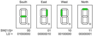
In the second half of the lab you will be using two (2) more switches and the same 7-segment display to show the direction you want your bear to walk. For example, if your bear is heading north, and enters a room requiring a right-hand turn (see Figure 5), then you would turn on segment b indicating that the bear should go East.
For this lab, we will use Switches 1 and 0 on the development board to input the direction we want the bear to go. These switches correspond to port pins PINC.1 and PINC.0 respectively. As before, we will assume that these port pins have been input to register r6 as illustrated in the arduino-proto-shield schematic. The logic value corresponding to each switch position is defined by variables dir.1 and dir.0. The following table translates these two switch positions into their corresponding dir input values and outputs signals to LED segments f, a, b, and g of the 7-segment display.
| Inputs | Outputs | |||||||
| Direction | SW1 | SW0 | dir.1 | dir.0 | Direction Segment ON = 1, OFF = 0 |
|||
| LDg | LDb | LDf | LDa | |||||
| South | DWN | DWN | 0 | 0 | 1 | 0 | 0 | 0 |
| East | DWN | UP | 0 | 1 | 0 | 1 | 0 | 0 |
| West | UP | DWN | 1 | 0 | 0 | 0 | 1 | 0 |
| North | UP | UP | 1 | 1 | 0 | 0 | 0 | 1 |
Continuing with our initial example; we have a bear in a room with north and west facing walls (SW[7:4] = 0101), we want the bear to go east (SW[1:0] = 01). For this situation the switches would be set as shown in the illustration below.
Now that we know what we want we will look at two different ways to implement it using our microcontroller.
Boolean Logic
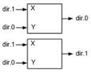
Applying what you learned in your Digital Logic Design class, construct a sum-of-products (SOP) expression for each direction segment. For our example, we would want to light the direction segment pointing east. All work should be included in your lab notebook.
To draw the Boolean equations in Microsoft Word select Insert – Equation …
Flowchart
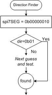
In the last section, you applied what you learned in EE201 “Digital Logic Design” to create your Boolean equations to calculate the segment to be turned ON. In this section, you will apply what you learned in your programming class and in pre-lab 1, to construct a flowchart to determine which segment to turn on based on dir bit 1 and bit 0. Specifically, you will translate the flowchart into a series of conditional statements. For example, if dir bit 1 is equal to 0 and dir bit 0 is equal to 1 then turn on bit 1 of register r8. From the introduction to this section (Direction Finder) we know this will turn on segment b (i.e., spi7SEG = 0b00000010).
Draw your flowchart using your favorite drawing program (Visio, Illustrator, etc.).
Part C – Questions
- A student flips the switches on their proto-shield, such that, switches 7, 2, and 0 are up, and the rest are down, as represented by the following blocks:

The student then runs ReadSwitches and executes the following assembly code:
clr r7
bst r6, 2
bld r7, 5
bld r7, 3
bst r6, 4
bld r7, 7
a. What is the binary value of register 6 (r6)?
b. What is the binary value of register 7 (r7)?
c. What is the value of the T bit in SREG? - The eighth bit of register 17 (bit # 7) needs to be moved into the fourth bit of register 18 (bit # 3).
a. Write two lines of code to achieve this task using bst and bld.
b. If the starting hexadecimal value of r17 is 0x7A, and the starting hexadecimal value of r18 is 0xEC, what will be the final hexadecimal value of r18 after performing your code? - A student is debugging their code for the proto-shield, and has tried to simulate a switch input as in problem 1. She has checked the following pins in the AVR simulator:


When she runs ReadSwitches, register 6 (R06) and the watch window for “switch” contain a hex value of 0x80.
a. Why does register 6 contain 0x80 and not 0x85?
b. Show how the student should have clicked the pins in AVR simulator:


What Should I Turn In?
Turn in the following material. The page numbers may change if you need more room for certain parts but the order must be followed. Points will be deducted if this instruction is not followed. Make sure all your original work is in your Lab Notebook. All written material must be typed or neatly done in ink. Once again please do not copy.
Page
- Title page with the pre-lab number, your name and picture, today’s date, and the day your lab meets.
- A completed version of the Figure 3 “Room Combinations” picture.
- Your assembly code from “Part 1 – Room Builder” Your code must be typed, but does not need to be assembled.
- Four (4) Boolean Expressions for the four direction segments
- A Flowchart of Direction Builder
- Questions and answers to all questions.
Lab 2A: Build a Test Bench Room Builder
Table of Contents
Introduction
As you hopefully remember from the previous lab, our long term objective is to help guide a bear through the following maze.
Towards that goal, in this lab you be writing code to create a software test-bench that can generate all the rooms by reading the left-most 4-switches, and turn on and off direction indicator LEDs based on the right-most 2-switches. To help you remember how everything should operate by the end of this lab, I have generated the following reference card.
PRINT OUT THE MAZE (FIGURE 1) AND THIS REFERENCE CARD (FIGURE 2) AND ALWAYS KEEP THEM WITH YOUR BOARD.
What is a Test Bench?
Over the semester, you will be writing assembly code subroutines to help our bear find his way out of the maze. But how do you know that a subroutine works unless you have built the whole thing? Testing subsystem elements has been a challenge since before computers were even invented. For electrical components, it was traditionally done on a “test bench” which was equipped with power supplies and signal generators to provide the input to the Device Under Test (DUT), also referred to as a Unit Under Test (UUT), and Volt Ohm Meters (VOM) and oscilloscopes to measure the output of the DUT. We have carried this nomenclature forward into the world of computer engineering.
To help us test our future software modules (DUTs), we will build a simple test bench comprised of switches to provide our inputs and the 7-segment display to let us view the output. As our design matures, we will no longer need our test bench and in fact in the latter labs you will not even use the switches. Specifically, in this lab, you will use the switches and seven-segment display to draw the different rooms that our bear may encounter in any maze and to provide him with directional information.
Ironically, one of the most difficult parts of any project is understanding what you (or the customer) want. Applying this principle to the task at hand, one of the most difficult parts of any lab is trying to understand what the instructor wants. To help you understand the overall objectives of a lab, I will from time-to-time include an “Owner’s Manual.” In these sections I will talk about how your program should operate when completed.
What is New?
Here are some of the new concepts you will be exploring in this lab.
- Working with Bits
- More on Simulation and Debugging
- Uploading to the Arduino
The following instructions and assembly directives are used in Labs 1 and 2. New items are underlined.
AVR Assembly Instructions
Data Transfer
mov r8, r7 // Move data from register r7 into register r8
in r7, PINC // Input port C pins (0x09) into register R7
out PORTB, r7 // Output to Port B from register R7
Arithmetic and Logic
clr r16 // Clear register r16
ser r17 // Set register r17
Control Transfer
call WriteDisplay // Subroutine Call
rjmp loop
Bit and Bit-Test
bst r7,7 // Bit store from register r7 bit 7 to SREG T bit
bld r8,6 // Bit load from SREG T bit to register r8 bit 6
AVR Studio Assembly
Directives
.DEF spiLEDS = r9 // Replace spiLEDS with the text r9
.EQU seg_a = 0 // Replace seg_a with the number 0
.CSEG // Code Segment
.ORG 0x0000 // Code Origin
.INCLUDE “spi_shield.inc” // “ “ means the file is in the project folder
.INCLUDE // < > means the file is in the AVR Studio folder
Labels
loop:
Comments
; // /* */
Working with the Arduino Shield
You will be using your Lab 1 spi_shield file for the remainder of the semester. Before we begin, let’s review how to use the subroutines included in spi_shield.inc.
To read the switches on the Arduino Shield, you call an assembly function named ReadSwitches which will return the state of the switches in register r6. To turn ON and OFF the 8 discrete LEDs on the shield, you write to register r8. To turn ON and OFF each segment of the 7-segment display, you write to register r7. To send the r8:r7 register pair to the Arduino Proto-shield, you call the WriteDisplay subroutine. The switches, LEDs, and 7-segment display on our Arduino Proto-shield implement positive logic, which means that for the switches UP = 1 and DOWN = 0, and for the lights ON = 1 and OFF = 0. Remember: changes made in the r8:r7 register pair (see Note 1) will not be displayed until you call WriteDisplay.
Note 1: The colon “:” means concatenate (i.e., combine) these two 8 bit registers to create a 16-bit register.
Create the Lab2 Project
If you are using a lab computer I would recommend erasing everything in Drive D and using this area for your project. Do not forget to save often. At the end of the lab do not forget to save to your Flash drive.
- Open AVR Studio and create a new Project named Lab2 (see Lab 1 for detailed instructions)
- Copy over your spi_shield.inc written in Lab 1.
- Copy the text in Lab1.asm into Lab2.asm
- Update the title block

- Build your project and verify you are starting with zero errors and zero warnings.
Add Software Wires to Make a Room
First delete the line wiring the switches to the seven segment display.mov r7, r6 // wire to 7-segment displayThis should leave only the line wiring the switches to the discrete LEDs. mov r8, r6 // wire to discrete LEDs Next make the changes to the code after the label loop as shown here.
 You should now be able to create all the rooms in the maze by toggling the 4 most significant switches. Let’s make sure by simulating your program.
Debug Workshop 3 – Simulate Your Program
You must complete this section before starting lab 3. You may/will be tested on the information contained in any Debug Workshop plus you will need to demonstrate proficiency with the simulator (i.e., debugger) as part of the sign-off for this lab sequence (both Parts A and B).
Once your program has assembled successfully enter AVR Studio’s debug mode by pressing the Assemble and Run ![]() icon.
icon.
If closed, expand the Registers folder in the Processor pane and PORTC and PORTD in the I/O View pane within AVR Studio. Select PORTD. In the window below the I/O View, and shown in Figure 1, you will notice that PORTD has three rows of eight bits, represented by square boxes.
Each box corresponds to a flip-flop or pin as defined in the table “Port Pin Configurations.”
| DDRXn | PORTXn | I/O | Pull-up | Comments |
| 0 | 0 | Input | No | Read “Synchronized” PINXn |
| 0 | 1 | Input | Yes | |
| 1 | X | Output | N/A | Write bit to PORTXn |
Looking at Figure 1, let’s start with the top row and the Port D Data Direction Register (DDRD). Each box in this row corresponds to flip-flop. As defined in Table 1, if this box is filled in (Flip-Flop DDRXn = 1) then this port pin will be an output. Conversely, if the box is not selected then the port pin will be an input. The second row of Figure 1 may be visualized as a physical Port D pin (PIND). If you want to simulate a change on an input pin, say from a switch being toggled, this is the box you would set (input = 1) or clear (input = 0). The third row contains the Port D register (PORTD). Each box in this row corresponds to flip-flop PORTxn. As described in Table 1, these flip-flops are interpreted differently based on if the port pin is defined as an input (DDRXn = 0) or an output (DDRXn = 1). If DDRXn = 0, then the corresponding PORTXn flip-flop adds (PORTXn = 1) or removes (PORTXn = 0) a Pull-up resistor (see fourth column in Table 1). If DDRXn = 1, then the corresponding PORTXn flip-flop defines the output state of the pin. If you want to see how your program modifies a pin defined as an output, PORTXn is the box you would look at.
For our application, all Port D pins are to be inputs with pull-up resistors assigned to the two most significant inputs wired to the two most significant (left-most) switches. In this case all the boxes in the DDRC (top row) would be empty (logic 0) and the two most significant boxes of the last row would be filled in (logic 1) as shown in Figure 1. Set a break-point at the line that calls our readSwitches subroutine.
![]()
Run to this line ![]() and verify that the PORTD registers have been initialized in Figure 1. Next simulate turning on the switch on the left by selecting the left most check-box in PIND. Now step over the call to readSwitches
and verify that the PORTD registers have been initialized in Figure 1. Next simulate turning on the switch on the left by selecting the left most check-box in PIND. Now step over the call to readSwitches ![]() . The subroutine still runs, AVR Studio simply does not show you the step-by-step details. Verify that register R06 = 0x80. This means ReadSwitches read PIND pin 7 and moved it into register r6.
. The subroutine still runs, AVR Studio simply does not show you the step-by-step details. Verify that register R06 = 0x80. This means ReadSwitches read PIND pin 7 and moved it into register r6.
Single step ![]() your program to the line…
your program to the line…
bld r7,6
Verify that the most significant bit of register r6 has been copied to the SREG T bit. Based on your program the other SREG bits may be different from the ones shown below. At this time we are only concerned with the T bit.
![]()
Now execute the line we are on and verify that the T-bit has been moved to bit 6 of register r7.
![]()
From our prelab we know that this corresponds to Segment g on our 7 segment display – a south facing wall
In a similar fashion, verify that the code you wrote in your pre-lab is wiring the other switches to their respective segments as defined in Figure 2.
Making Your Code More Readable
Open the spi_shield.inc file (double-click in Project window) in AVR Studio.

As touched on in Lab 1 and covered in more detail here in Appendix A, the m328pdef.inc include file makes our code more readable by the use of equates (.EQU) and define (.DEF) assembly directives. The equate assembly directive performs a numeric substitution. Simply put, whenever the assembler encounters text which has an equate assigned to it, it replaces the text with the numeric value defined in the equate statement. For example, in m328pdef, the text PORTD is equated to the number 0x0b.
.EQU PORTD = 0x0b
Consequently, whenever the assembler encounters the text PORTD it substitutes the number 0x0b.
The define (.DEF) assembly directive works in a similar fashion performing a textual substitution. Simply put, whenever the assembler encounters text which has a define statement assigned to it, it replaces the text with the text value in the define statement. For example, in m328pdef, the text XH is defined as meaning the text r27.
.DEF XH = r27
Consequently, whenever the assembler encounters the text XH it substitutes the text r27. Following the lead of m328pdef, I have added a few definition and equates of my own in spi_shield.inc to make working with the proto-shield a little easier.
; SPI interface registers
.DEF spiLEDS=r8
.DEF spi7SEG=r7

; Switches
.DEF switch=r6

; 7-segment display
.EQU seg_a=0
.EQU seg_b=1
.EQU seg_c=2
.EQU seg_d=3
.EQU seq_e=4
.EQU seg_f=5
.EQU seg_g=6
.EQU seg_dp=7
To read the switches on the Arduino Shield you call readSwitches which returns the state of the switches in register r6. Now, instead of writing r6 to look at the switches you can use the more descriptive word switch, which means the same thing (.DEF switch=r6). To turn ON and OFF the 8 discrete LEDs on the shield you used to write to register r8. Now you can use the more descriptive mnemonic spiLEDs (.DEF spiLEDS=r8).
For example here is the instruction wiring the switches to the discrete LEDs.
mov r8, r6 // wire to discrete LEDs
By replacing the register numbers with the more descriptive mnemonics the instruction becomes much more understandable.
mov spiLEDS, switch // wire to discrete LEDs
Now lets make your code more readable. When specifying a single discrete LED bit, the number of the bit was clear enough (7, 6, 5,… 0). For the 7-segment display knowing which segment is which is a little more confusing. The final series of equates lets you specify the segment (bit) you want to work with by name (seg_dp, seg_g, seg_f, …seg_a) as defined in Figure 3 7 Segment display.
Now let’s use our newly created define assembly directives to make our code more readable. For example the two lines wiring the leftmost switch with its corresponding south wall segment…
bst r6,7 // wire switch 7 to segment g (south wall)
bld r7,6
now becomes much more readable..
bst switch,7 // wire switch 7 to segment g (south wall)
bld spi7SEG,seg_g
Following my example rewrite your code to make it more understandable.
This completes Lab 2A. You will be continuing with this code in Lab 2B. The submission for Lab 2 is the combination of both Lab 2A and 2B.
You are finally ready to upload and test your program on your Arduino.
How to Upload your Hex file using AVR Dude
If you have not done so already, download and install AVR Studio, WinAVR, and Arduino IDE from http://www.atmel.com/dyn/products/tools_card.asp?tool_id=2725, http://sourceforge.net/projects/winavr/, and http://arduino.cc/en/Main/Software
If you are running Windows 7 and have an Arduino Duemilanove (not an Arduino Uno) you may need to download the Virtual COM Port Drivers from Future Technology Devices, used by the winAVR software to upload programs to your board.
At this time you should have verified that your Arduino works by uploading and running blink from the Arduino IDE (Integrated Development Environment) and that the Protoshield works by running sketch_shiftOut_16-bit. Instructions are provided in “How to Build the Arduino Proto-Shield.”
Open notepad from your computer and type in the following two commands:
avrdude -p m328p -c arduino -P \\.\COM4 -b 115200 -U flash:w:Lab2.hex
pause
You will need to confirm which com port the Arduino UNO is using, so you may have to change it from COM4 to the correct number. Additionally, the file name has to match exactly. If you named your project lab_2, the file name to use will be lab_2.hex .
In order to save the file as a batch file in the same folder as the project, make sure to add .bat to the end of the name and make sure that the Save as type option is set to all files instead of text document. You can name the batch file whatever you like but it is suggested to be upload328P.bat . You can copy this file and make modifications to the contents in order to upload future labs.
Here is a short description the options and how you will need to modify them. For a complete list of avrdude command line options go to http://www.nongnu.org/avrdude/user-manual/avrdude_4.html#SEC4 her
-p partno Use -p ? option in the command window (Windows - R Open:cmd) to get a list of part numbers
-c programmer-id You can also use stk500v1
-P port Set to your port number. The \\.\ provides support for com port numbers greater then 7.
-b baudrate For the Arduino Uno keep the baud rate at 115200. For the Arduino Duemilanove change the baud rate to 57600
-U memtype:op:filename[:format] Enter the name of your file (ex. Blink.hex)
memtype flash The flash ROM of the device.
op w Read the specified file and write it to the specified device memory.
In the future if you need to create a new batch file or if you modified this one; be sure to save the file with a .bat extension (not .txt) in the folder containing your hex file (look in the folder named ‘default’).
To find your port number, in the control panel open the Device Manager, expand Ports (COM & LPT). Look for the Arduino, it should say something like USB Serial Port (COM4).
![]()
Using Notepad change the port setting in the upload.bat file to this port number.
To upload your program run the batch file (right-click open or double-click). For the Arduino Duemilanove you may to simultaneously press the reset button. The order is not important; but both must be done within less than a second of each other. Don’t panic if you get it wrong. You will simply see the message including the text “not in sync.” Wait until you see the line “Press any key to continue . . .” press any key and then try again.
Appendix A The m328pdef Include File
Open the m328pdef.inc file (double-click in Project window) in AVR Studio.

Each port register (DDRXn, PORTXn, and PINXn) has its own unique address within both the Data Memory and I/O area of the ATmega microcontroller as defined in Table A.1. For this lab we will use the I/O address of each of our ports.
Table A.1 General Purpose Digital I/O Port Register Definitions
You can find the original version of this table in the ATmega328P doc8161.pdf document in Section 30 “Register Summary.” A similar version is in Appendix B ATmega328P Registers and specifically, Section B.1 Register Summary of your textbook. The I/O address of each register is shown on the left (see Table above). The Data Memory address is shown in parenthesis. For example, you can input register PINC from the address 0x06. Where the 0x simple means this is a hexadecimal number (0x06 = 0616).
While we could use the actual address in our assembly instruction; our code is more readable if we use its mnemonic (i.e., PINC = 0616). The “equating” of these mnemonics with their corresponding values is done in the m328pdef.inc “include” document. This is a text document so you can open it in AVRStudio or even Notepad at any time and take a look at what is going on under the hood. Here is the relevant section for our ports…
.EQU PORTD = 0x0b
.EQU DDRD = 0x0a
.EQU PIND = 0x09
.EQU PORTC = 0x08
.EQU DDRC = 0x07
.EQU PINC = 0x06
.EQU PORTB = 0x05
.EQU DDRB = 0x04
.EQU PINB = 0x03
The “dot” tell the assembler that this line is talking to the assembler and not to be turned into a machine instruction. The mnemonic equ tells the assembler to make the following equate. For example, the first line would tell the assembler to replace PORTD with the value 0B16 whenever it comes across it in the assembly code portion of the program.
To have the assembler read (include) the m328pdef.inc text file we use the include assembly directive. One again an “assembly directive” is an instruction to the Assembler; in contrast with an Assembly instruction which the assembler turns into an ATmega328P machine instruction.
.INCLUDE
Because it is so important to remember when a line is intended for the Assembler (Assembly Directive) and when a line is to be converted to a machine instruction intended for the ATMega328P microcontroller (Assembly Instruction), I always capitalize Assembly Directives and place in lower case letters Assembly Instructions. AVR Studio is not case sensitive, so this convention is not required for your assembly program to assemble correctly – it is however required by the instructor.
Lab 2B — Build a Test Bench Direction Finder
Please quickly scan the lab before starting. This is a new class of lab that you can tailor to your own learning and academic goals. Specifically, you can follow a step-by-step or do-it-yourself approach – you decide. You can also decide how simple or difficult you would like to make the lab, based on the grade you would be happy receiving.
Table of Contents
Introduction
In the first part of this lab (Lab 02A) you designed a circuit with four (4) switches wired to four (4) LEDs of the 7-segment display. Using the four switches you were then able to draw all 16 rooms that the bear might encounter in his journey through the maze. This was the beginning of building your test bench to be used to verify the code you will write in future labs.
In the second part of the lab (Lab 02B) your goal is to design a digital circuit with two (2) switches that will turn on one of the rooms 4 LED segments indicating the direction you want your bear to walk. Like the previous lab, this code will become an important component of your test bench.
What is New?
Here are some of the new concepts you will be exploring in this lab.
- More Working with Bits
- Logical Instructions
- Conditional Branch Instructions
The following instructions and assembly directives are used in Labs 1 to 2. New items are underlined.
AVR Assembly Instructions
Data Transfer
ldi r16, 0x03 // Load immediate the number 3 into register r16
lds r16, dir // Load data from SRAM variable room into register r16
sts dir, r16 // Store data from register r16 into SRAM variable room
mov r8, r7 // Move data from register r7 into register r8
in r7, PINC // Input port C pins (0x09) into register R7
out PORTB, r7 // Output to Port B from register R7
Arithmetic and Logic
cpi a, 0x03 // compare immediate a with 0x03
cbr r16, 0xF0 // Logical and of r16 with complement of constant 0xF0
or r16, r17 // logical bit-wise or of r16 and r17, result placed in r16
com r16 // complement (not) of register r16
clr r16 // Clear register r16
ser r17 // Set register r17
Control Transfer
brne next_test // branch is not equal to label next_test
call WriteDisplay // Subroutine Call
rjmp loop
Bit and Bit-Test
brts next_test // Branch if T set
swap r5 // Swap high and low nibbles in register r5
bst r7, 7 // Bit store from register r7 bit 7 to SREG T bit
bld r8, 6 // Bit load from SREG T bit to register r8 bit 6
AVR Studio Assembly
Directives
.DSEG // Data Segment
.BYTE 1 // reserve 1 byte in SRAM
.DEF spiLEDS = r9 // Replace spiLEDS with the text r9
.EQU seg_a = 0 // Replace seg_a with the number 0
.CSEG // Code Segment
.ORG 0x0000 // Code Origin
.INCLUDE “spi_shield.inc” // “ “ means the file is in the project folder
.INCLUDE // < > means the file is in the AVR Studio folder
Labels
loop:
Comments
; // /* */
Review and a few new pieces of the puzzle
Configuration
Here is how the top-level configuration section of your program should look.
;
 /* Lab2.asm - Show a Room
 * Version 1.0 <- update this number each time you print your program
 * Created: 1/27/2013 11:01:03 AM
 * Author: Your Name Here
 * Lab: Tu 7:00pm - 9:45pm
 */

.INCLUDE

.CSEG
.ORG 0x0000

RST_VECT:

rjmp reset // jump over IVT, tables, and include file(s)

.ORG 0x0100 // bypass IVT

.INCLUDE "spi_shield"
Lets take a look at this code, with an eye to reviewing what we have learned to date, while adding a few more pieces to the puzzle.
Title Block
The title block provides a top-level description of the program and information about who wrote it.
INCLUDE
The include assembly directive (.INCLUDE) tells the assembler to load the text file m328pdef.inc at this point in the code. This is a simple block copy-paste operation. If it is not already open, open the m328pdef.inc file located in the Included Files folder in the Project window pane (left side of window). If you do not see it you may need to expand the folder (click the + box) or build the project (click the ![]() Assemble icon). If all else fails you can open the file directly. From the menu bar select Project and Open File. Navigate to and select C:\Program Files\Atmel\AVR Tools\AvrAssembler2\Appnotes\m328Pdef.inc. This file is unique to your AVR microcontroller and provides useful mnemonics for mapping AVR standardized mnemonics with their respective locations in the data and i/o address space.
Assemble icon). If all else fails you can open the file directly. From the menu bar select Project and Open File. Navigate to and select C:\Program Files\Atmel\AVR Tools\AvrAssembler2\Appnotes\m328Pdef.inc. This file is unique to your AVR microcontroller and provides useful mnemonics for mapping AVR standardized mnemonics with their respective locations in the data and i/o address space.
CSEG and ORG
The code segment assembly directive (.CSEG) tells the assembler we are about to start writing assembly instructions to be translated into machine code and placed into program memory.
The origin assembly directive (.ORG) immediately following, tells the assembler that we want it to start placing this code at location 0x0000 in code memory.
When you press the reset button on the Arduino the reset pin on the AVR microcontroller is placed at logic 0 and the Program Counter (PC) begins executing the first instruction at program address 0x0000 (RST_VECT) .
For us the first instruction executed is a jump instruction to the code identified by the label reset (rjmp reset).
Notice that another origin assembly directive (.ORG 0x0100) places this code after location 0x0100. This is done to place our program code after the AVR’s Interrupt Vector Table (IVT) which we will learn about in the future. Between the .ORG 0x0100 directive and the start of your code is another .INCLUDE directive. Which was first introduced in Lab 2. If you have already forgotten Lab 2, here is a quick review.
.INCLUDE “spi_shield”
While the Arduino Duemilanove board is a great low priced microcontroller board it is i/o pin poor. Specifically, it does not include enough general purpose i/o pins to support our 8 switches, 8 discrete LEDs, the 8 pins needed for the 7-segment display, and the other miscellaneous components that make up our Proto-Shield. To solve this problem the shield uses the Serial Peripheral Interface (SPI) of the AVR microcontroller. You will learn about this peripheral device in the future but to minimize your confusion I have hidden it inside the spi_shield.inc file. As before, the assembler simply does a block copy of the material in this file and pastes it at this point in the program.
If you open the spi_shield include file, you will see it includes some definitions (.DEF) and equates (.EQU). Unlike definition (.DEF) assembly directives, equate (.EQU) directives do a numeric substitution. For example, in our program anywhere the assembler sees “seg_a” it will replace it with the number 0. Like the define directive the equate directive is used to add clarity to our assembly program. Looking around you will also see three subroutines (InitShield, ReadSwitches, and WriteDisplay and SpiTxWait). In the language of C++ you can think of InitShield, WriteDisplay, and ReadSwitches as public and SpiTxWait as private. Which means we will call InitShield, WriteDisplay, and ReadSwitches from our main program.
SRAM Variable Definition
Now might be a good time to let AVR Studio know about an SRAM variable named dir. Add the following two lines just after the first .INCLUDE assembly directive.
.INCLUDE

.DSEG
 dir: .BYTE 1

.CSEG
.ORG 0x0000

RST_VECT:

rjmp reset

.ORG 0x0100 // bypass IVT

.INCLUDE "spi_shield.inc"
DSEG and BYTE
This is the first time we have placed anything into SRAM, so lets take a closer look at what is happening. The .DSEG assembly directive tells the AVRStudio assembler that we are going to be talking about the Data Segment (DSEG). This is just another way of saying SRAM Data Memory. The .BYTE assembly directive tells the AVRStudio assembler that we want to reserve N bytes of RAM whose starting address should be associated with the specified name. In this example the variable named dir and the number of bytes to be associated with this name is 1.
Initialization
Here is how the initialization (reset) section of your program should look.
reset:

 ldi r16, low(RAMEND) // RAMEND address 0x08ff
 out SPL, r16
 ldi r16, high(RAMEND)
 out SPH, r16

; Initialize Stack, and GPIO Ports, and SPI communications
 call InitShield
The reset section initializes our stack (see Lab 2 “Stack Pointer Initialization”), and configures our SPI peripheral device by calling the InitShield subroutine included with spi_shield.inc.
Variable Initializations
A good programming practice is to initialize all variables on reset. Within the reset section of your program lets set variable dir equal to the number 3 (hex 0x03).
ldi r17, 0x03 // your descriptive comments here
sts dir, r17
Highlight in yellow your descriptive comments. Please do not simply repeat the name of the mnemonic instruction. For example, for the mnemonic instruction ldi r6, 0x03 do not write the comment “load imediate register r16. In this example, the load immediate (ldi) instruction is paired with the store in sram (sts) instruction on the next line. The purpose of this pair of instructions is to initialize the direction variable so the bear is facing north (0x03). Therefore, a good comment would be something like “the bear enters the maze facing north”
It would be nice if we could simply set variable dir directly equal to the number 3. However, this is not how a load-store architecture works. The idea behind our RISC architecture is that instructions operate on registers not variables in memory. If you want to therefore perform some operation with a variable you need to…
- Load the data (e.g., lds, ldi, in),
- Do something (typically an arithmetic or logical instruction), and then…
- Store (sts, out) the result.
We are initializing variable dir so we do not care what their current value is and can therefore skip the load (lds) step. The selection of register r16 is somewhat arbitrary. For example in place of register r16, I could have chosen any register between r16 and r31.
Loop
We finish our review with the main loop.
loop:
 ; SPI Software Wires

call ReadSwitches
mov spiLEDS, switch // wire to discrete LEDs

clr spi7SEG // start with all 7-segments OFF

bst switch, 7 // wire switch 7 to segment g (south wall)
bld spi7SEG, seg_g
...
call WriteDisplay
rjmp loop
The main loop section of our program clears the 7-segment display and discrete LEDs, reads the switches, implements the “software wires” used to manually build a room. The program ends with an rjmp, which repeats the process.
Direction Finder
In this section you are going to write the code to turn on the 7 segment LED corresponding to the direction the bear is currently facing.
Some Electrical Engineers are more comfortable working with truth tables and Boolean logic, others prefer writing programs using conditional expressions, while a few like programming challenges. In this lab you can choose which path you take. Specifically, you may choose to program your direction finder using one of three different approaches.
- Your Boolean expressions from the pre-lab.
- Your flowchart from the pre-lab.
- Model the Arduino C++ solution by creating a one-dimensional array and using the indirect addressing mode to translate the direction. (design challenge)
The maximum number of points you can receive on a lab is governed by which approach you select. These points are estimates only and may be adjusted by the instructor.
| Design | Basic Lab (points) |
Design Challenge | Total Possible |
| Boolean Logic | 16 | 4 | 20 |
| If-Then Flowchart | 17 | N/A | 17 |
| If-Then-Else | 17 | N/A | 17 |
| Indirect Addressing | 20 | N/A | 20 |
Regardless of which option you choose, the first thing that needs to be added to your code is updating the newly created direction variable with the value from the direction switches in the main loop. Place the following lines of code after the clr spi7SEG.
mov r16, switch // move switch (r7) to temporary register r16
cbr r16, 0xFC // mask-out most significant 6 bits
sts dir, r16 // save formatted value to SRAM variable dir.
These three lines of code are taking the input from the switches, clearing out the unused bits and saving it to the dir variable. By doing this, the user can quickly get the direction value from the dir variable instead of taking it from the switches and clearing out the unused bits every time.
Programming Option 1: Convert your Digital Logic Expressions into Subroutines
For this solution you will be translating the Boolean expressions from your pre-lab into assembly code. To translate each Boolean expression into assembly code you will use AVR 8-bit logical instructions com, and. Because you are implementing only one gate at a time, you will only need 1 of the 8 bits. For my example I have arbitrarily picked bit 0. To help you get started here is the the code needed to decode 7-segment LED segment b.
loop:
 ; SPI Software Wires

 call ReadSwitches
 mov spiLEDS, switch // wire to discrete LEDs

 mov r16, switch // move switch (r7) to temporary register r16
 cbr r16, 0xFC // mask-out most significant 6 bits
 sts dir, r16 // save formatted value to SRAM variable dir.
 ...
 call WriteDisplay

 ; Lab 2 Direction Finder

 lds r16, dir // load direction into temporary register r16
 clr spi7SEG // start with all 7-segments OFF

 ; facing east (segment b)

 mov r18, r16 // your comments here
 bst r16, 1
 bld r17, 0

 // B = /A * B
 com r17 // your comments here
 and r18, r17

 bst r18, 0 // store answer into T
 bld spi7SEG, seg_b // load answer from T into segment
Bits versus Bytes
For this lab I want to implement a series of logical expressions, working with one bit at a time. The AVR processor logical instructions work with bytes and not bits. If you think about it, this is not really a problem. For example, in the above code, I work with bit 0 and simply do not worry about the other bits.
We begin by loading the direction the bear is currently facing (SRAM variable dir) into scratch pad register r16 and making sure all our 7-segment display elements (LEDs) are off (at logic zero).
Our initial objective is to move bit 0 into register variable B bit 0. This one is easy, Direction bit 0 is already in bit 0 of register r16 so I can simply move it to register r18. Direction 1 is a little trickier. In this case I move bit 1 into bit 0 through the T bit in the status register sreg. This is the technique you first learned about in Lab 3. I then use the 8-bit logic instructions to implement my Boolean expression – again I am only interested in bit 0. It is important to note that the left hand operand (in this case r18) of any arithmetic and logic instruction acts as both a source and a destination. Consequently, the original source bit(s) are destroyed.
Once you understand how my “digital logic gate” works, write the missing parts of the program for the remaining 3 segments (g, f, and a). If you need to, refer to the Arduino Proto-Shield schematic for switch and 7-segment LED assignments.
 ; facing south (segment g)
 mov r18,r16
 bst r16,1
 bld r17,0

Write your direction code (translating your circuit schematics from the prelab) for segments g here along with your comments.

 bst r18,0 // store answer into T
 bld spi7SEG,seg_g // load answer from T into segment

 ; facing west (segment f)
 mov r18,r16 // your comments here
 bst r16,1
 bld r17,0

Write your direction code (translating your circuit schematics from the prelab) for segment f here along with your comments.

 bst r18,0 // store answer into T
 bld spi7SEG,seg_f // load answer from T into segment

; facing north (segment a)
 mov r18,r16 // your comments here
 bst r16,1
 bld r17,0

Write your direction code (translating your circuit schematics from the prelab) for segments a here along with your comments.

 bst r18,0 // store answer into T
 bld spi7SEG,seg_a // load answer from T into segment

 call WriteDisplay
 rjmp loop
Verify the basic operation of the program using AVR Studio. For detailed step-by-step instructions see Debug Workshops 1, 2, and 3. Remember, before you debug/run any program you should know what values will be contained in the affected registers.
Design Challenge for Option 1 – Byte Implementation
Some of you find the material difficult enough and appreciate step-by-step instructions, while others like to figure things out for themselves. This section is designed for the later group. If you are happy with your basic solution please proceed to the next section and decide if you want to accept the design challenge.
The code provided in this and future labs is designed for instructional purposes and may not be as optimized for size and speed as possible. This optimization of code is the primary reason that engineers program in assembly versus a high level language like C++. It is also one of the things that makes assembly programming so much fun for many engineers. If you like a challenge, then see if you can rewrite the above code to make it smaller and faster.
The code provided in lab requires 28 instructions to implement. My “optimized” solution to this coding problem only takes 16 instructions to do the same thing. I limited my optimized solution to only use instructions you already know, including bst (4), mov (1), com (1), bld (8), and (1), cbr (1). The number in parenthesis is the number of times my minimum solution used the instruction.
I was able to optimize the code by observing that I was always working with bit 0 and forgetting about the other 7 bits in the register. But what if I aligned the bits to be operated on based on the segment to be turned on or off. If I were to rewrite my code in this fashion I would only need a single and instruction, thus greatly simplifying my program, while also adding clarity.
If you like challenges, see if you can implement my parallel solution, or come up with an even better solution.
Programming Option 2: Implement your Flowcharts using an “If-Then” Binary Tree Structure
In the last section you applied what you learned in EE201 “Digital Logic Design” to create your Boolean equations to calculate the segment to be turned ON. In this programming based solution you will apply what you learned in your programming class, to construct a flowchart to determine which segment to turn on based on dir bit 1 and bit 0. Specifically, you will translate the flowchart you built in the pre-lab into a series of conditional If-Then statements. For example, if dir bit 1 is equal to 0 and dir bit 0 is equal to 1 then turn on bit 1 of register r8. From the introduction to this section (Direction Finder) we know this will turn on segment b (i.e., spi7SEG = 0b00000010).
Begin by replacing each decision diamond with a compare bit store (bst) instruction and a brts conditional branch if T flag set instruction. The bst instruction saves the bit to be tested to the T bit in SREG. We then test this bit using the brts instruction. As a general rule use the complementary form of the conditional branch in your decision diamond. For example, if you want to branch if dir bit 1 (dir.1) is clear you would use the brts instruction as shown here.
 lds r16, dir // move direction bit 1 (dir.1)
 bst r16, 1 // into SREG T bit
 brts case1X // your comment here
 bst r16, 0
 brts case01
 ; code to be executed if bit 1 and 0 are zero (case00)
 ; 7 segments gfedcba
 ldi r16, 0b01000000 // spi7SEG = r8, seg_g = 1
 rjmp found

 case01:
 ; code to be executed if bit 1 and 0 = 01
 ; 7 segments gfedcba
 ldi r16, 0b00000010 // spi7SEG = r8, seg_b = 1
 rjmp found

case1X:
; more code and comments...

found:
mov spi7SEG, r16
Programming Option 3: Implement your Truth Table using an Optimized “If-Then-Else” Structure
Compare Immediate (cpi) Instruction
For this solution you will be using the compare immediate instruction to implement the conditional expression in the Table 1.
| Inputs | Outputs | |||||||
| Direction | SW1 | SW0 | dir.1 | dir.0 | Direction Segment ON = 1, OFF = 0 |
|||
| LDg | LDb | LDf | LDa | |||||
| South | DWN | DWN | 0 | 0 | 1 | 0 | 0 | 0 |
| East | DWN | UP | 0 | 1 | 0 | 1 | 0 | 0 |
| West | UP | DWN | 1 | 0 | 0 | 0 | 1 | 0 |
| North | UP | UP | 1 | 1 | 0 | 0 | 0 | 1 |
For this solution each line of the truth table becomes a guess, followed by a compare immediate cpi instruction, and finally a conditional branch instruction.
The Guess
In assembly, it’s all about code optimization. One technique assembly programmers use with conditional expressions to optimize code is to guess an answer and then test for the condition. If the guess was correct then no additional work is required. This typically results in simpler and less confusing code which runs as fast or faster (if the guess was correct) than the more traditional approaches. Here is how our flowchart for seg_b would look applying this technique.
Notice that the code is more linear than the if-then binary tree solution. Here I guess that the return value will be 0b00000010. Specifically, segment seg_b is on with all other segments off. For this to be true, the bear would need to be facing East (dir = 0b01). If my guess is correct then I can jump to my found label. Now lets look at the assembly code needed to implement this flowchart.
Code Example
The code provided here implements the direction finder flowchart defined above. Note: 0b01 assumes that the leading bits are zero and therefore 0b01 = 0b00000001.
 lds r16, dir ; load direction bear is facing into r16
 ; 7 segments gfedcba
 ldi r17, 0b00000010 ; guess bear is facing east (seg_b = 1)
 cpi r16, 0b01 ; if bear is facing east then we are done
 breq found
 ; 7 segments gfedcba
 ldi r17, 0b01000000 ; guess bear is facing south (seg g = 1)
 cpi r16, 0b00 ; if bear is facing south then we are done
 breq found
 ; more code and comments...

found:

mov spi7SEG, r17 ; transfer correct guess to 7 segment register
When comparing the above code with the flowchart one difference you will immediately notice is that the ldi instruction only works with registers r16 to r31 and spi7SEG is in r8, which means we can not directly place our “guess” in r8. Instead I will temporarily place my guess in r17 and only when I reach the found label move r17 (the correct guess) into r8 (spi7SEG).
Programming Option 4: Implement the Arduino C++ Solution in Assembly
This is a design challenge solution, which simply means less instructional information is provided and the solution requires the use of assembly instructions not yet covered in class. Design challenges were created as a response to students who requested more open-ended problem definitions.
Open the Lab02B.ino file within the Arduino IDE. Here the direction segment is chosen by first creating a one-dimensional array of segments (g, b, f, and a). The location of each segment within the array corresponds to the direction the bear is facing. For example, looking at Table 1 above if you are currently facing South (dir = 00), then you want to turn on segment g. Therefore, in the lookup table, the first entry is segment g. Here is the C++ code.
static const byte truth_table[] = {_BV(seg_g), _BV(seg_b),_BV(seg_f),_BV(seg_a)};
 seg7_val |= truth_table[dir_val];
The macro _BV(bit) is defined as 1<<bit.The symbol << being the C left shift operator. In words, the compiler is directed to shift the number 0x01 to the left bit tiresulting a Byte Value (BV) with a 1 in the bit position. For example, _BV(6) would equal 0b01000000. Our assembler does not support the Byte Value (_BV) macro, so we will substitute its definition (1<<bit)
Create the array in assembly using the Define Byte (.DB) assembly directive. Access the array using the indirect addressing mode instruction lpm.
RST_VECT:
 rjmp reset // jump over IVT, tables, and plus INCLUDE code
 .ORG 0x0050 // bypass IVT
 dir_table: .DB 1<<seg_g, 1<<seg_b,="" 1<<seg_f,="" 1<<seg_a<="" em=""></seg_g,>

 .ORG 0x0100 // bypass IVT
 .INCLUDE "spi_shield.inc"
Lab 2 Deliverable(s)
STOP Read the Lab READ ME document contained in the Labs Folder. Be absolutely sure you have followed all instruction in the “Lab Formatting” section of this document. Points will be deducted if you do not follow these instructions. You have been warned.
Make sure your lab notebook is up to date. Follow the guidelines provided in the “Lab Notebook” section of the Lab READ ME document.
Make sure you have read and understand the “Plagiarism” section of the Lab READ ME document, especially if you are repeating the class.
All labs should represent your own work – DO NOT COPY.
Pre-Lab 3: Subroutines
Table of Contents
Before you begin I recommend reviewing the Introduction to Lab 02
In this Lab you will begin by writing four (4) subroutines. TurnLeft, TurnRight, TurnAround, and HitWall. These four subroutines are the subject of this pre-lab. After you have completed these four subroutines you will write two new subroutines named RightPaw and LeftPaw. These two subroutines will illustrate the power of subroutines by simply using the previously written subroutines to answer the questions “Did the bear’s right paw touch a wall?” and “Did the bear’s left paw touch a wall?”
Teaching the Bear to Turn Left, Turn Right, and Turn Around
In the first part of this Lab you are going to teach the bear how to change directions – turn left, turn right, and to turn around. Let’s first consider the TurnLeft subroutine (i.e, pseudo-instruction).
| Facing Direction | Direction after turning Left | ||||
|---|---|---|---|---|---|
| dir.1 | dir.0 | dir.1 | dir.0 | ||
| x | y | ||||
| South | 0 | 0 | East | 0 | 1 |
| East | 0 | 1 | North | 1 | 1 |
| West | 1 | 0 | South | 0 | 0 |
| North | 1 | 1 | West | 1 | 0 |
Note: The syntax dir.1 is a shorthand way of saying variable dir bit 1.
As an example, if the bear is facing north (dir = 11) and you tell him to turn left, then after calling the TurnLeft subroutine, he should be facing west (dir = 10).
As you did in the previous lab, the above table can be viewed as a truth table with inputs dir and outputs dir.
Having variable dir for both input and output can be a little confusing so I have added x as a pseudonym for inputs dir.1 and y for dir.0 and broken the problem into two blocks as shown above and represented as two truth tables. Again inputs dir bit 1 (dir.1) and dir bit 0 are now renamed x and y respectively.
|
|
||||||||||||||||||||||||||||||||||||
Boolean Logic
Applying what you learned in your Digital Logic Design class construct a sum-of-product (SOP) expression for each table entry (min term). To review, begin by writing a product expression for each one (1) in the output . These are the input conditions where you want to produce an output of 1. In other words, if the first condition OR the second input condition are true (1) you want to output a 1. This reasoning leads directly to our first SOP expression for Table 1.
Now write the SOP expression for dir.1 shown in Table 2.
dir.1 = ?
Simplify your two expressions (dir.1 and dir.0) by observation or using Boolean algebra. You may find it helpful to refer to this Basic Laws and Theorems of Boolean Algebra document. Please, do not draw a 2 variable Karnaugh map. Include all your work in your lab notebook.
Distributive Law
Law of Complements
Dual of Identity Law
After all that work you can, by simple observation, see that our solution is correct. To draw the Boolean equations in Microsoft Word select Insert – Equation …
Flowchart
Applying what you learned in your programming class construct a flowchart for subroutines TurnLeft, TurnRight, and TurnAround. Each flowchart should show how to determine a new value for variable dir based on the current value of dir. For example, if I am writing the flowchart for TurnLeft I will start by testing if dir is equal to 0x00. If it is the bear is facing south and because I want the bear to turn left I will set variable dir equal to 0x01.
Did the Bear Hit a Wall?
Reading: Before you begin this part of the pre-lab, you may want to review Chapter 1 of your textbook on logical operators. For this pre-lab you will need to understand AVR Logical Instructions COM, AND, OR, and EOR by reading about each in AVR Studio’s Assembler Help document.
- Complete the following truth table.
Table 4: Switch to LED0 Truth Table Input Output Logic Gate Selected SW1 SW0 LED0 AND 0 0 0 1 1 0 1 1 OR 0 0 0 1 1 0 1 1 EOR (Exclusive OR) 0 0 0 1 1 0 1 1 COM(Inverter) 0 1 To give you a little practice using the Assembler Help window in AVR Studio (Help – Assembler Help), look-up the CBR and SBR instructions. Use the information from the help provided for these two instructions to answer the following two questions.
- The Clear Bit(s) in Register (CBR) instruction performs what logical operation to clear individual bits in a register?
- The Set Bit(s) in Register (SBR) instruction performs what logical operation to set individual bits in a register?
- What byte-wide logical instruction can be used to test if a bit or bits are set? You only need to indicate the appropriate operator. Do not worry about the entire instruction. (IE the focus is on MOV from MOV R7, R6) To help you answer this question, consider the following drawing depicting 8 2-input gates.

The type is unknown at this time so I have simply drawn 8 boxes. I then named one of the inputs to each of the gates “test.” To test if a bit or bits are set (bn = 1), you set the corresponding “test” bit to 1. If any of the bit or bits being tested is 1 the corresponding output will be a non-zero value.
In the following example I want to see if bit 1 in register r24 is set. Consequently, I would set bit 1 in my “test” byte (register r16) to 1. The answer is no so the contents of output register r24 is zero.

- Write the single logical instruction that would be used to test the bits, using inputs R19 and R24. R19 and R24 are two of the AVR’s 32 8-bit general purpose registers. Assume r24 initially contains the byte you want to test, and register r19 contains the test sequence (in our example 000000102). The output of the test should be into R24.
- What would the contents of R26 be after the instruction COM R26 is executed if it originally has the value 0b11001010?
What Should I Turn In?
Turn in the following material. Make sure all your original work is in your Lab Notebook. All written material must be typed or neatly done in ink. Once again please do not copy.
Page
- Title page with the pre-lab number, your name and picture, today’s date, and the day your lab meets.
- Truth tables and simplified Boolean expressions for TurnLeft, TurnRight, and TurnAround
- Flowcharts for TurnLeft, TurnRight, and TurnAround You may use more than one page to show your flowcharts
- The problem statements (remove explanatory text) and solutions to the five (5) pre-lab questions in Part B of the pre-lab. Circle and/or highlight your answers. Make sure all your original work is located in your lab notebook. This part of your pre-lab must be typed. You may use more than one page to write the question and answer these five questions.
Lab 3A: Pseudo-instructions TurnLeft, TurnRight, and TurnAround
Ironically, one of the most difficult parts of any project is understanding what you (or the customer) want. Applying this principle to the task at hand, one of the most difficult parts of any lab is trying to understand what the instructor wants. To help you understand the overall objectives of a lab, I will from time-to-time include an “Owner’s Manual.” In these sections I will talk about how your program should operate when completed.
Owner’s Manual
As you hopefully remember from the previous labs, our long term objective is to help guide a bear through the following maze.
Towards that goal, you have already written test-bench code that can generate all the rooms by reading the left-most 4-switches, and turn on and off direction indicator LEDs based on the right-most 2-switches. To help you remember how everything should operate up to this point I have generated the following reference card.
If you have not done so already (Lab 2), print out the maze and reference card above. I highly recommend keeping these open and on your desktop when doing any of the labs.
You may have already noticed that I have included two new switches on the reference card named “turn.” The purpose of the switches is to test pseudo-instructions TurnLeft, TurnRight, and TurnAround which you worked on in the pre-lab and will now implement in lab. To test these three new pseudo-instructions you will write a subroutine named WhichWay which will call the three new pseudo-instructions based on the position of the turn switches as shown in the reference card. For example, let’s say the direction switches are both in the up position (11). By the compass on the card we see that this means the bear is facing North (n), If you completed Lab 2 correctly, then segment-a should be ON. For our example, we want to see if pseudo-instruction TurnLeft is working. By looking at the card we see that, to simulate turning left we need to set the switches to UP = 1 and DOWN = 0. If pseudo-instruction TurnLeft is working then the bear should now be facing west and consequently segment-a should be OFF and segment-f should now be ON. To completely verify the functionality of the TurnLeft pseudo-instruction you will need to test it for all four (4) directional cases (initially facing North, South, West, and finally East). Do not get confused. Turns are always made relative to the direction the bear is facing. That means if the bear is facing south and you are testing the TurnRight pseudo-instruction then segment-d should turn OFF and segment-f should turn ON.
Table of Contents
What is New?
Lab 03 represents a reset of the lab sequence. Specifically, I am providing subroutine versions of the in-line code you wrote in Labs 01 and Lab 02. These subroutines named DrawRoom and DrawDirection are located in a new include file named testbench. Like almost all the subroutines you will be writing in this and future labs, they are C++ compliant by using register r24 for sending arguments and returning function values.
To work with my two new subroutines, I am providing a new Lab03 assembly file and the testbench.inc file. While functionally equivalent to your Lab 2 program, Lab03 calls both of my new subroutines.
You do not need any code from previous labs.
AVR Assembly Instructions
Here are some of the new instructions you will be learning in this lab.
Data Transfer
push r16 // place register r16 onto the stack
pop r16 // remove register r16 from the stack
Control Transfer
brts cond_01 // branch if T is set
rcall WhichWay // relative subroutine call
Bit and Bit-Test
lsr r24 // shift contents of r24 right by 1 bit
Lab03.asm code
; ---------------------------------------- ; Lab 3 - Pseudo-instructions ; Version 1.1 ; Date: February 10, 2017 ; Written By : Your Name ; Lab Hours : Tuesday 7:00pm - 9:45pm ; For questions regarding this code, contact your email address ; ---------------------------------------- .INCLUDE.DSEG room: .BYTE 1 // Defines the SRAM variable called room dir: .BYTE 1 // Defines the SRAM variable called dir .CSEG .ORG 0x0000 RST_VECT: rjmp reset // jump over IVT, plus INCLUDE code .ORG 0x0100 // bypass IVT .INCLUDE "spi_shield.inc" .INCLUDE "testbench.inc" // DrawRoom and DrawDirection reset: ldi r17,HIGH(RAMEND) // Initializes Stack Pointer to RAMEND address 0x08ff out SPH,r17 // Outputs 0x08 to SPH ldi r16,LOW(RAMEND) out SPL,r16 // Outputs 0xFF to SPL call InitShield // initialize GPIO Ports and SPI communications clr spiLEDS // clear discrete LEDs clr spi7SEG // clear 7-segment display ;Initialize SRAM Variables clr r17 // initializes r17 to 0 and then stores data from r17 into variable room sts room, r17 ldi r17, 0x03 // loads the hex number 3 into r17 and then stores that value into variable dir sts dir, r17 loop: call ReadSwitches // read switches into r6 // dir = switch & 0x03; mov r17, switch // move switch (r6) to temporary register r17 cbr r17, 0xFC // mask-out most significant 6 bits sts dir, r17 // save formatted value to SRAM variable dir. /* Read Switches and update room and direction */ // room = switch >> 4; mov r17, switch // move switch (r6) to temp register r17 cbr r17, 0x0F // mask-out least significant nibble swap r17 // swap nibbles sts room, r17 // save formatted value to SRAM variable room. /* Draw Direction */ lds r24, dir // calling argument dir is placed in r24. rcall DrawDirection // translate direction to 7 segment bit mov spi7SEG, r24 // Displays DrawDirection on the 7 segment display. call WriteDisplay /* Room Builder */ lds r24, room // calling argument room is placed in r24. rcall DrawRoom // translate room to 7-seg bits mov spi7SEG, r24 // return value, the room, is saved to 7 segment display register call WriteDisplay // display the room rjmp loop
testbench.inc code
; ----------------------------------------
; Testbench Utility
; Version 1.1
; ----------------------------------------

;directions (most significant 6 bits zero)
.EQU south=0b00
.EQU east=0b01
.EQU west=0b10
.EQU north=0b11

; --------------------------
; --- Draw the Room ---
; input argument in r24 is the room
; return value in r24 is the room formatted
; for a 7-segment display
; No general purpose registers are modified,
; while SREG is modified by this subroutine.

DrawRoom:

	push   reg_F 	        // moving this register onto the stack so
	in     reg_F,SREG       // it can be used to save the value in SREG
	push   r17

        mov    r17, r24         // move input to temporary register
	cbr    r24, 0b11111100  // room bits 1 and 0 are already aligned to segments b and a
        cbr    r17, 0b11110011
	swap   r17
        lsr    r17              // room bits 3 and 2 are now aligned to segments g and f
	or     r24, r17         // SW7:SW4 now mapped to 7 segment display

	pop    r17 		// restore original contents of r17
	out    SREG,reg_F
	pop    reg_F
	ret

; --------------------------
; --- Set Direction Bit ---
; The input argument in r24 is the direction
; and return value in r24 is the 7-segment display
; no registers are modified by this subroutine

DrawDirection:
	push  reg_F
	in    reg_F,SREG
	push  r16

        mov   r16, r24          ; move direction bear is facing into r16
        ldi   r24, 1<
        cpi   r16,south         ; if bear is facing south then we are done
        breq  found
        ldi   r24, 1<
        cpi   r16,west          ; if bear is facing west then we are done
        breq  found
	ldi   r24, 1<
        cpi   r16,east          ; if bear is facing east then we are done
        breq  found
        ldi   r24, 1<

found:
	pop    r16
	out    SREG,reg_F
	pop    reg_F
	ret
Create the Lab3 Project
If you are using a lab computer I would recommend erasing everything in Drive D and using this area for your project. Do not forget to save often. At the end of the lab do not forget to save to your Flash drive.
- Open AVR Studio and create a new Project named Lab03.
- Copy over the code for Lab03.asm that was provided above.
- Create a new file and copy over the code for testbench.inc. Make sure to save it with that exact name.
- Within windows, copy over your version of spi_shield.inc from Lab02.
- Within windows, copy over your upload.bat from Lab02. Open the text file in notepad (right-click edit) and change the file name from Lab02.hex to Lab03.hex
- Update the information in the title block.
- Build your project and verify you are starting with zero errors and zero warnings.
Subroutines TurnLeft, TurnRight, and TurnAround
SRAM Variable turn
Before we write our first three subroutines, let’s define and initialize a new variable in SRAM named turn.
- Applying what you learned in Lab 02B “SRAM Variable Definition,” define a new variable named turn.
- Applying what you learned in Lab 02B “Variable Initialization,” initialize your new SRAM variable too.
Now that the assembler knows what the word turn means and the AVR processor has initialized it, we can use it in our code.
The least significant two bits of SRAM variable turn will hold the values in switches SW3 and SW2.
In the following code taken from Lab03, each block of code is preceded by its C++ equivalent. You may want to open the Lab04A.ino sketch within the Arduino IDE to see these C++ statements in context. To help you write the code to extract the variable turn from the switch input, I have again included the C++ code equivalent.
Comparing the preceding lines of code you can see we have pretty much done the same thing for SRAM variables room, and dir. Specifically, we moved the switch values into a temporary register (r16), masked out the bits we will not be using (cbr), and then we used different bit manipulation instructions to right justified the remaining bits. For the turn variable you will again follows these steps. For the bit manipulation you will need to right justified switches SW3 and SW2 by using the logical shift right instruction twice. In C++ this is double shift is accomplished with the shift operator (>> 2). In assembly this is done by using the logical shift right instruction (lsr) twice. As the name implies, this instruction shifts the contents of the source/destination register by 1 bit, while shifting 0 into the most significant bit.
loop:

; Test Bench

call ReadSwitches // read switches into r7

/* Read Switches and update room, direction, and turn */

// dir = switch & 0x03;
 mov r17, switch // move switch (r6) to temporary register r16
 cbr r17, 0xFC // mask-out most significant 6 bits
 sts dir, r17 // save formatted value to SRAM variable dir.

// room = switch >> 4;
 mov r17, switch // move switch (r7) to temporary register r16
 swap r17 // swap nibbles
 cbr r17, 0xF0 // mask-out most significant nibble
 sts room, r17 // save formatted value to SRAM variable room.

// turn = (switch >> 2) & 0x03;
 … write your assembly code with comments here.
 ...
 rjmp loop
Write Subroutines TurnLeft, TurnRight, and TurnAround
In this section you are going to write subroutines TurnLeft, TurnRight, and TurnAround.
You may now choose to write each subroutine using one of three different approaches.
- Your Boolean expressions from the pre-lab.
- Your flowcharts from the pre-lab
- Model the Arduino C++ solution by creating a one-dimensional array and using the indirect addressing mode to translate the direction. (design challenge)
The maximum number of points you can receive on a lab is governed by which approach you select. These points are estimates only and may be adjusted by the instructor.
| Design | Basic Lab (points) | Design Challenge | Total Possible |
| Boolean Logic | 15 | 2 | 17 |
| Flowchart | 15 | 2 | 17 |
| Indirect Addressing | 20 | N/A | 20 |
As you work through your own solutions do not forget to show all your work in your lab notebook.
Rules for Working with Subroutines
Please read Appendix A “Rules for Working with Subroutines” at the end of this lab for rules you must always follow when writing subroutines. I have included this material as an Appendix so you may more quickly review it in subsequent labs.
Place the following empty subroutines TurnLeft, TurnRight, and TurnAround just after the main section of your code.
 ; -------------------------------------
 ; -------- Pseudo Instructions --------
 ; --------------------------
 ; ------- Turn Left --------
 ; Called from WhichWay subroutine (see Table 5.1)
 ; The input and output is register r24
 ; register SREG is modified by this subroutine
 TurnLeft:

Your AVR Instructions and comments here
 ret

; --------------------------
 ; ------- Turn Right -------
 ; Called from WhichWay subroutine (see Table 5.1)
 ; The input and output is register r24
 ; register SREG is modified by this subroutine
 TurnRight:

Your AVR Instructions and comments here
 ret

; --------------------------
 ; ------- Turn Around -------
 ; Called from WhichWay subroutine (see Table 5.1)
 ; The input and output is register r24
 ; register SREG is modified by this subroutine
 TurnAround:

Your AVR instructions and comments here
 ret
Highlight in yellow your descriptive comments. Please do not simply repeat the name of the mnemonic instructions as I have done in the TurnLeft sample code (next section). I did this to help you learn the instructions. In practice I would have written the comment differently. For example, for the mnemonic instruction mov r16, r24 I would have written something like,
/* Register r24 is used as both an input and an output. The remaining code works with r24 as an output. Consequently, I am moving the input to scratch pad register r16. */
It is good programming rule, not to mention making your subroutine much more portable, to protect registers modified by your subroutine. In the spirit, of simplifying the course/lab I have not enforced this rule – up to this point. Subroutine TurnLeft uses register r16 as a temporary register. Following our new rule I have saved the value in r16 onto the stack before my subroutine modifies it. I then restore the original value before I exit the subroutine. You should not save/restore registers used to return values.
It is now time to decide which path you wish to follow in implementing your pseudo-instructions. You may want to quickly read over the next three sections before deciding which path you want to take.
Programming Option 1: Convert your Digital Logic Expressions into Subroutines
In this section I will show you how to translate each simplified SOP expression, generated in the pre-lab, into assembly code. As you hopefully discovered, this can be done with a little bit manipulation and the complement (com) instruction. I have included my TurnLeft subroutine to help you get started. As you can see, each result is accomplished by moving bits through our 1-bit T flag in the Status Register (SREG).
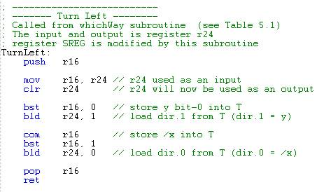
Programming Option 2: Convert your Flowcharts into Subroutines
Translate your flowcharts, generated in the pre-lab, into assembly code. Begin by replacing each decision diamond with a compare immediate cpi and a conditional branch instruction. As a general rule use the complementary form of the conditional branch in your decision diamond. Here is my TurnLeft subroutine to help you get started.

To help make the code more readable I introduced the following equate statements in the testbench include file provided with this lab. Do not add these to your assembly file.
;directions (most significant 6 bits zero)
 .EQU south=0b00
 .EQU east=0b01
 .EQU west=0b10
 .EQU north=0b11
Programming Option 3: Implement the Arduino C++ Solution in Assembly
This is a design challenge solution, which simply means less instructional information is provided and the solution requires the use of assembly instructions not yet covered in class. Design challenges were created as a response to students who requested more open-ended problem definitions.
Open the Lab03A.ino file within the Arduino IDE. Here the turn left and right subroutines are implemented by first creating a one-dimensional array of directions. The location of each direction within the array corresponds to the turn to be made. Once created to make a turn you only need to use the direction, a number from 0 to 3, as an index into the array. For example, looking at Table 1 from the pre-lab if you are currently facing South (dir = 00), and you turn left you will end up looking East (dir = 01). Therefore, in the turn left array, you want the first entry to be East.
| Facing Direction | Direction after turning Left | ||||
|---|---|---|---|---|---|
| dir.1 | dir.0 | dir.1 | dir.0 | ||
| x | y | ||||
| South | 0 | 0 | East | 0 | 1 |
| East | 0 | 1 | North | 1 | 1 |
| West | 1 | 0 | South | 0 | 0 |
| North | 1 | 1 | West | 1 | 0 |
Create the array in assembly using the Define Byte (.DB) assembly directive. Access the array using the indirect addressing mode instruction lpm.
WhichWay – Testing the T flag
To find out if your pseudo-instructions work, you are going to write a new subroutine named WhichWay. Call WhichWay from the main program just after moving the SRAM variables dir and turn into temporary registers r24 and r22 respectively. Unlike your in-line code written in Labs 1 and 2, our subroutines do not work directly with variables dir and turn. Instead these variables are loaded into registers r24 and r22 and then sent as arguments to WhichWay. Subroutine WhichWay also does not change the variable dir directly. Instead, it returns the new direction value in register r24, which we then store in variable dir. We are doing this for two reasons. First, it makes our subroutines more general purpose, allowing them to possibly be used in other parts of our program and second it allow our assembly programs to be called from a top level C++ program. Add the following code to the main loop right after the section that updates the SRAM variables.
// turn = (switch >> 2) & 0x03;
… write your assembly code with comments here.
...

; Direction Finder

 lds r24, dir   // load direction bear is facing into r24
 lds r22, turn  // load direction bear is to turn into r22
 rcall WhichWay // change direction based on variable turn
 sts dir, r24   // save formatted value to SRAM variable dir.

; Draw Direction

   lds r24, dir        // calling argument dir is placed in r24.
   rcall DrawDirection // translate direction to 7 segment bit
   mov spi7SEG, r24    // Displays DrawDirection on the 7 segment display.
   call WriteDisplay
We will be using switches 3 and 2, now right justified and located in register r22 bits 1 and 0 respectively to input which action we want the bear to take as defined by the following table.
| r22 bit 1 |
r22 bit 0 |
action |
| 0 | 0 | do not turn |
| 0 | 1 | turn right |
| 1 | 0 | turn left |
| 1 | 1 | turn around |
Step-by-Step Instructions for writing WhichWay
- Let’s begin with the header block so we will know how to use our subroutines. Although you may place this subroutine anywhere after the rjmp loop instructions, I would recommend placing it right at this point.

Like all subroutines the last instruction is always return (ret). - The basic objective of our WhichWay subroutine is to translate two switch bits into four subroutine calls. One way to accomplish this is by testing each bit at a time as shown in the following flow chart. This is the same technique used in Pre-lab 02 to determine the room number the bear had entered.
I began by testing bit 1, if it is one (1) then I know that I am looking at condition (cond) 112 or 102. At this point I do not know which so I will label this point cond 1X, where the X could be 1 or 0. Following this path I next test bit 0. If it is 1 then I know I have condition 112 and I need to turn around. If it is 0 then I have condition 102 and I need to turn left. The 0X condition follows a similar train of logic.
Now we have to turn our flowchart into assembly code. The key is the use of the branch if T set (brts) instruction. Here is the start of my version of WhichWay. I use my handy bst instruction to sequentially copy each switch value into the T flag and branch based on its value (1 or 0) using the brts instruction.

Repeat the above strategy to implement the cond_1X one bit test and then branch to conditions 10 and 11 (cond_10 and cond_11) accordingly.
Design Challenge – Dueling Subroutines (2 points)
You can skip this section if you are happy receiving a passing or even a good grade on the lab. If you want to receive an excellent grade you will need to accept the challenge. If you implemented the third solution (one-dimensional array with indirect addressing mode) then you should skip this design challenge.
Create a new Project named Lab03C. Copy the contents of your Lab03.asm file into your new Lab03C.asm file. Place a copy of your spi_shield.inc and testbench.inc files along with the upload.bat file into your new project folder. Update the file name in the upload.bat file. Build your project and verify you are starting with zero errors and zero warnings.
Using the Programmer’s Reference Card (Figure 2) and the following switch assignments, we would know that the bear was going North when he entered a room with North and West facing walls. Given no choice, the bear is instructed to turn right. Run the program on your Arduino and verify that this is in fact what happens.

What if we had not told the bear to turn right, but instead had taken no action and let the bear continue north.

Enter these switch settings and see what happens. At first you will probably not see any difference; however, if you look a little closer you will see that segment a is a little brighter than the others. What is going on? The part of your code which builds the room is interfering with the code which generates the direction. Both program elements modify the same bits in spi7SEG register r8 before calling WriteDisplay, so one may turn a segment on while the other turns it off.
Your challenge is to solve this problem. For my solution I defined a byte in SRAM named room7segment.
.BYTE room7segment 1
Variable room7segment is different from variable room. The latter holds a 4-bit value corresponding to the room number, while the former contains the actual LEDs to be turned on or off. Do not get confused.
I then replaced spi7segment with an instruction to save the room to be displayed in variable room7segment in my room builder program. Next I deleted the first call to WriteDisplay. Next I wrote a new subroutine named Display; replacing my last call to WriteDisplay with this new subroutine. In my new Display subroutine I combined room7segment and spi7SEG using a logical or instruction.
lds r24, room7segment
 or spi7SEG, r24
Now if a room or direction LED is on it stays ON. Now all I needed to do was call WriteDisplay before returning to the calling program.
This is a design challenge so you may run into problems. If you do, don’t forget to use the simulator to help you figure out what is going wrong.
Appendix A Rules for Working with Subroutines
In the last lab I introduced three steps for writing a program for a load-store RISC based architecture.
- Load the data (lds),
- Do something (typically an arithmetic or logical instruction), and then…
- Store (sts) the result.
When working with subroutines an analogous set of steps applies.
- Load argument(s) into input registers (parameters) specified in the header of the subroutine. Following the gcc C++ calling convention, this would be register r24 if only one calling argument is specified (lds r24, myData).
- Call the Subroutine
- Do something with the return value(s) stored in the output register(s) specified in the header of the subroutine. Following the gcc C++ calling convention, this would be register r24 if a single byte value is returned. In most cases you will storing this return value(s) into SRAM data memory (sts myData, r24).
You call a subroutine using the rcall or call assembly instruction and return using the ret instruction. Here are a few rules to remember when writing your main program and subroutines.
- Your subroutine should always include a header block. As a minimum, the header must define the input arguments to the subroutine, the values returned, and what if any registers are modified by the subroutine.
- Always initialize variables and registers at the beginning of your program. Do not re-initialize variables or registers within a loop or a subroutine. For example, you only need to configure the port pins assigned to the switches once.
- Never jump into a subroutine. Use a call instruction to start executing code at the beginning of the subroutine.
- Never jump out of a subroutine. Your subroutine should contain a single return (ret) instruction as the last instruction.
- You do not need an ORG assembly directive. As long as the previous code segment ends correctly (rjmp loop, ret, reti) your subroutine can start at the next address.
- Subroutine names start with a capital letter.
- Your subroutine should contain only one return instruction (ret, reti) located at the end of the subroutine (last instruction). All blocks of code within the subroutine should exit the subroutine through this return (ret).
- Push (push r7) any registers modified by the subroutine at the beginning of the subroutine and pop (pop r7) in reverse order the registers at the end of the subroutine. This rule does not apply if you are using one of the registers or SREG flags to return a value to the calling program. Comments should clearly identify which registers are modified by the subroutine.
- You cannot save the Status Register SREG directly onto the stack. Instead, first push one of the 32 registers on the stack and then save SREG in this register. Reverse the sequence at the end of the subroutine.
push r15
 in r15, SREG
 :
 out SREG, r15
 pop r15
- Once again, never jump into or out of a subroutine from the main program or any other subroutine. However, subroutines may call other subroutines.
Lab 3B: Pseudo-instruction HitWall, LeftPaw, and RightPaw
This lab sequence (3a and 3b) is all about subroutines. In part one (Lab 3a) you were given two new subroutines named DrawRoom and DrawDirection, which implemented your code from Labs 1 and 2. In part A of this lab, you wrote your first three pseudo-instructions (implemented as subroutines) named TurnLeft, TurnRight and TurnAround. In addition to these three new pseudo-instructions you wrote a subroutine named WhichWay to test them. Hopefully by now you realize that subroutines can clean up your code and make it more readable. In part one (lab 3A) you also learned a few rules about how to make a nice general purpose subroutine.
In this second part of the lab you will now discover that subroutines can act as building blocks in the construction of more complex programs. Specifically, you will now use subroutines DrawRoom, DrawDirection, TurnLeft,and TurnRight in more than one place to solve what initially may appear as an unrelated problems.
First, you will use the two subroutines I provided to you (DrawRoom and DrawDrection) to write a new general purpose subroutine named HitWall. You will then write two new subroutines named LeftPaw and RightPaw using subroutines TurnRight, and TurnLeft from lab 3A and your new HitWall. One unexpected benefit you will discover, is that you can write all these new subroutines (HitWall, LeftPaw,and RightPaw) while only needing to learn a few new assembly instructions (and, tst).
Table of Contents
What is New?
Here are some of the new concepts you will be exploring in this lab.
- Application of a general purpose subroutine
Here are some of the new instructions you will be learning in this lab.
AVR Assembly Instructions
Arithmetic and Logic
tst r24 // r24 = r24 & r24
and r24, r16
Pseudo-instruction HitWall
In this part of the lab you are going to start helping the bear to explore a room by answering the question “Did you hit a wall?” Within your assembly program you will ask the question by calling a new subroutine named HitWall. To answer the question, your new subroutine will need to know the room the bear is currently in and the direction the bear is facing. This information is saved in variables room and dir respectively.
While the subroutine could directly load variables room and dir, we will continue to follow our programming practice of sending arguments as required by the gcc C++ compiler for mixed C++/Assembly programming.
Sending Arguments as Required for Mixed C++/Assembly Programming
In a mixed C++/Assembly application program, the first argument is sent in the r25:r24 register pair, the second in r23:r22, the third in r21:r20, etcetera. In the past, now, and in the future we will assume the most significant register of the pairs (r25, r23, r21,…) are zero. For our HitWall subroutine we will somewhat arbitrarily send the direction dir variable in r24 and the room in r22. So how do these variables get in the registers? The answer to this question leads to the basic structure of all our subroutine calls.
lds r24, dir // first argument
lds r22, room // second argument
call HitWall
In a similar fashion to the calling arguments being sent in these register pairs, function return values are returned in the same registers in the same sequence – r25:r24 register pair, the second in r23:r22, the third in r21:r20, etcetera.
Write a new subroutine named HitWall using register r22 (room) and register r24 (dir) as arguments and using byte-wide logical operators (com, and, or) such that if the answer to the question is no (the bear did not hit a wall) the r24 register is set to zero.
Conceptually, we want to first, using our new subroutines DrawDirection, and DrawRoom, convert SRAM variables dir (now in register r24) and room (now in r22) into their respective 7-segment images. Now that the bits have been aligned to a segment we want to test if the bit set to 1 in r24 (a wall in the room) corresponds to a bit set to 1 in r16 (the direction the bear is facing). If it is, we want to set the register r24 to a non-zero value. I have provided the C++ equivalent statement as a comment to help you get started.
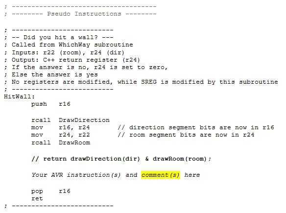
Write a Subroutine to Test HitWall
To find out if your new HitWall pseudo-instruction works, add the following call to TestHitWall in your main loop after the bear’s direction has been updated from WhichWay. The TestHitWall as the name implies a temporary subroutine we are adding simply to verify the operation of the HitWall subroutine. As such it has no calling arguments and will itself load up the arguments for our HitWall subroutine.
In the following test code, I send the answer to the question to two of the discrete LEDs on the Arduino Proto-Shield. This is a great way to track your programs as they become more complex.
This is a temporary subroutine only intended to test if the HitWall subroutine works. For this reason the subroutine does not have to be callable from C++ and therefore does not follow our rules for passing arguments in registers (e.g. r24, r22).
Place your TestHitWall in the test subroutine area of your code.
Update Code

The above subroutine introduces the “Test for Zero or Minus,” mnemonic tst instruction. The tst instruction, like the compare instruction, is used to modify SREG flag bits, without modifying any operands. For our test, we are interested in the zero flag, which will be set if r24 = 0, and 1 otherwise. We then test the Z flag bit using the branch if equal (breq) instruction in order to take the correct action (turning on and off two test LEDs).
Test the HitWall Subroutine using the Proto-shield
As you have hopefully learned, it is always a good idea to test your code as often as possible. Using the TestHitWall subroutine test your HitWall subroutine on the protoshield. If it does not work simulate the program and locate the bug. The next two subroutines you will write call HitWall, so if it does not work, neither will they.
Pseudo-instructions RightPaw and LeftPaw
Our programming goal in this part of the lab is to continue to help the bear explore a room. Specifically, we now want to teach the bear to answer the questions “Can your right paw touch a wall?” and Can your left paw touch a wall?”
Here is my RightPaw subroutine using subroutines TurnRight and HitWall as building blocks . If the answer to the question is yes (the paw touches a wall) then I return a value not equal to zero.
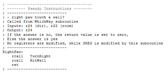
By using RightPaw as a guide, write LeftPaw.
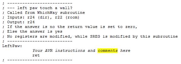
Test RightPaw and LeftPaw using the AVRStudio Simulator
Verify the basic operation of your RightPaw and LeftPaw subroutines using the AVR Studio Debugger. Remember, before you debug/run any program you should know what values will be contained in the effected variables (RAM) and registers. In this case you want to
- Run to ReadSwitches
- Set the maze and direction switches (your choice)
- Set a breakpoint at the entry to both RightPaw and LeftPaw.
- Watch r22 and r24
- Step over each subroutine and see if register r24 is being correctly set to TRUE or FALSE based on the switch positions you set.
- If you are not getting the answer you are expecting, reset the simulator, repeat steps 1 to 5, and this time step into the subroutine to be debugged. If everything looks good, repeat steps 1 to 5 until you are happy that your subroutines are working.
Test RightPaw and LeftPaw using the Proto-shield
Using my TestWall code from the previous lab as an example, write two new test subroutines named TestRightPaw and TestLeftPaw, to find out if your two new pseudo-instructions RightPaw and LeftPaw really work. Send the answers to the questions to four new discrete LEDs on the Arduino Proto-Shield board as defined below. Notice that an LED will light if the answer is yes or no. This allows positive feedback whether or not your subroutine is even being called. For example, if you only had an LED light up if the answer was yes, how would you know the difference between a subroutine that was never called and a subroutine that was called but always returned no?
Call TestRightPaw and TestLeftPaw from your main loop as shown below.
loop:
     /* start of the loop (readswitches, update variables) */
     sts turn, r17
     lds r24, dir
     lds r22, turn
     rcall WhichWay
     sts dir, r24
     rcall TestHitWall
     rcall TestRightPaw
     rcall TestLeftPaw

     /* Draw Direction */
     lds r24, dir
     rcall DrawDirection
     ....
     /* other code */

     ....
     call WriteDisplay
     rjmp loop
Using AVR Studio, simulate your new Test programs and then download and test your completed program. Like you, I always just download and then test. I mean who wants to wait! And like you the first time I tested my new subroutines they did not work. In AVR Studio I first set and ran to a break point at rcall DrawRoom. I did this to make sure my I/O ports had been configured. I then set my pin values on Ports D and C to match my switch settings and ran to a break point at the end of my program rjmp loop. I then looked at register r9 (spiLEDS) to confirm that what I saw on the board was what I saw in the simulator. That is a good thing; because, it means that I can find the bug using the simulator. I then set a break point at the beginning of TestRightPaw so I could single step and watch my test bench and new subroutines in action.
Debug Tips
Run a simulation on the main loop – enter a value and see if the output matches the simulation. If yes you can isolate quickly to the problem. If not you are missing something. Verify r8 and r9’s value every time WriteDisplay is called.
Common mistakes… Subroutines must input and output r22 and r24 only!!!! They must not modify any other registers like spi7SEG, spiLED, r8, or r9. They must not call WriteDisplay. The registers must be updated after the calls along with you call to WriteDisplay. Do not clear any registers like r8 or r9 within the main loop or in the subroutines. Verify that the stack does not change within the main loop. Again try and find out how or if the simulation output is different from what you are seeing on the upload version.
Design Challenge and Creative Corner
If you have not completed the Lab 3 Design Challenge or the Creative Corner; defined at the end of Lab3a you may do so at this time.
Lab 3 Deliverable(s)
STOP Read the Lab READ ME document contained in the Labs Folder. Be absolutely sure you have followed all instruction in the “Lab Formatting” section of this document. Points will be deducted if you do not follow these instructions. You have been warned.
Make sure your lab notebook is up to date. Follow the guidelines provided in the “Lab Notebook” section of the Lab READ ME document.
Make sure you have read and understand the “Plagiarism” section of the Lab READ ME document, especially if you are repeating the class.
All labs should represent your own work – DO NOT COPY.
Table of Contents
- Basic Lab
a. Main Program (Title Block, Initialization, Main Loop)
b. Subroutines (WhichWay, LeftPaw, HitWall, TurnRight, TurnAround, TestHitWall, TestRightPaw, and TestLeftPaw) - Design Challenge – Turn using Indirect Addressing Mode or Display
Pre-Lab 4A: Polling
Table of Contents
- The ATmega328P is equipped with two 8-bit timer/counters and one 16-bit counter. These Timer/Counters let you…
- Turn on or turn off an external device at a programmed time.
- Generate a precision output signal (period, duty cycle, frequency). For example, generate a complex digital waveform with varying pulse width to control the speed of a DC motor
- Measure the characteristics (period, duty cycle, frequency) of an incoming digital signal
- Count external events
Nomenclature
Frequency
The number of times a particular event repeats within a 1-s period. The unit of frequency is Hertz, or cycles per second. For example, a sinusoidal signal with a 60-Hz frequency means that a full cycle of a sinusoidal signal repeats itself 60 times each second, or every 16.67 ms. For the digital waveform shown, the frequency is 2 Hz.
Period
The flip side of a frequency is a period. If an event occurs with a rate of 2 Hz, the period of that event is 500 ms. To find a period, given a frequency, or vice versa, we simply need to remember their inverse relationship, where F and T represent a frequency and the corresponding period, respectively.
Duty Cycle
In many applications, periodic pulses are used as control signals. A good example is the use of a periodic pulse to control a servo motor. To control the direction and sometimes the speed of a motor, a periodic pulse signal with a changing duty cycle over time is used.
Duty cycle is defined as the percentage of one period a signal is ON. The periodic pulse signal shown in the Figure 1 is ON for 50% of the signal period and off for the rest of the period. Therefore, we call the signal in a periodic pulse signal with a 50% duty cycle. This special case is also called a square wave.
Timer 1 – Normal Mode Operation (default)
In lab you will be using the timer subsystems of the ATmega328P to generate a square wave with a frequency of 2 Hz.
We will be working with 16-bit Timer/Counter 1 due to the large delays (250 msec) needed to generate our 2 Hz frequency square wave. To keep things as simple as possible we will be operating Timer 1 in its default Normal mode. In this mode the counting direction is always up (incrementing). The counter overruns when it passes its maximum 16-bit value (MAX = 0xFFFF) and then restarts from the BOTTOM (0x0000). In normal operation the Timer/Counter Overflow Flag (TOV1) will be set in the same timer clock cycle as the TCNT1 becomes zero.

The TOV1 Flag in this case behaves like a 17th bit, except that it is only set, not cleared.

Maximum Delay
So can TCNT1 generate the 250 ms delay required to generate our 2 Hz square wave? To answer that question we will need to determine the maximum delay possible. Assuming a system clock frequency of 16.000 MHz and a prescale divisor of 64, the largest time delay possible is achieved by setting both TCNT1H and TCNT1L to zero, which results in the overflow flag TOV1 flag being set after 216 = 65,536 tics of the Timer/Counter1 clock.
fT1 = fTclk_I/O/64, given fTclk_I/O = fclk then fT1 = 16.000 MHz / 64 = 250 KHz
and therefore T1max = 65,536 tics / 250 KHz = 262.14 msec
Clearly, Timer 1 can generate a delay of 250 msec. Our next step is to calculate the TCNT1 load value needed to generate a 250 ms delay.
Step to Calculate Timer Load Value (Normal Mode)
To generate a 250 msec delay assuming a clock frequency of 16 MHz and a prescale divisor of 64.
Variables
tclk_T1 – Period of clock input to Timer/Counter1
fclk – AVR system clock frequency
Solution
- Divide desired time delay by tclk_T1 where tclk_T1 = 64/fclk = 64 / 16.000 MHz = 4 µsec
250msec / 4 µs = 62,500 - Subtract 65,536 – step 1
65,536 – 62,500 = 3,036 - Convert step 2 to hex.
3,036 = 0x0BDC
For our example TCNT1H = 0x0B and TCNT1L = 0xDC
Question 1 What values would need to be loaded into TCNT1H and TCNT1L to generate a 38 ms delay with a system clock frequency of 10.000 MHz and a prescale divisor of 8 (show your work)?
Initialization
Applying what we learned lets setup our timer to set overflow flag TOV1 after 250 ms.
ldi r16,0x0B // load value high byte (Sect 15.2-15.3)
sts TCNT1H,r16
ldi r16,0xDC // load value low byte
sts TCNT1L,r16
In the next step we simultaneously turn on the clock to Timer 1, and apply a prescaler of 64, as defined in Table 7.10: Timer1 Clock Select Bit Description in your textbook.
; Initialize Timer/Counter1
ldi r16,(1<<cs11)|(1<<cs10) // prescale of 64 Sect 15.11.2
sts TCCR1B,r16 // Table 15-5 Clock Select Bit Description
The C++ bit-wise left shift operator
The C++ bit-wise left shift operator << is used to move a one (1) into a specified bit location within a byte. In the first half of the expression an 8-bit value is built with the CS1 bit 1 set to 1 ( 0b00000010). In the second half of the expression an 8-bit value is built with the CS1 bit 0 set to 1 ( 0b00000001). The C++ bit-wise or operator | is used to combine these two bytes to form the byte to be stored in register r16 (0b00000011).
Question 2 The first two lines of code set both CS11 and CS10 bits to 1 in Timer 1 register TCCR1B, while setting all other bits to zero. What hexadecimal value is saved in TCCR1B? Register TCCR1B is shown in Figure 9-18 TCCR1B (Timer 1 Control) Register of your textbook. If you do not have the textbook you can also find this register in Section 15.11.2 TCCR1B – Timer/Counter1 Control Register B in the ATmega328P_doc8161 pdf file found in the reference folder on my website. Once you find register TCCR1B locate bits CS11 and CS10 and set these to one (1), set all other bits to zero (0). Convert this binary number to hexadecimal and you have the answer.
Polling
At this point the timer has been initialized so it will set the overflow flag TOV1 in the TIFR1 register after 250 ms, and the timer’s clock has been started.
Polling the overflow flag TOV1 is a very simple way to keep track of time. Specifically, with a polling routine we loop until the overflow flag bits is set (TOV1 = 1), once this event occurs, we know the desired time has elapsed.
Question 3 Write a small assembly subroutine named delay to poll the TOVF1 flag. When the flag is set (TOV1 = 1), clear theTOV1 flag by writing a 1 (sbi TIFR1, TOV1), and reset the timer value (TCNT1H:TCNT1L = 0x0BDC). You may think I just made a mistake by saying write a 1 to the TOV1 flag to clear it – but this is in fact how you clear a flag within the ATmega architecture. Do not ask me why.
Question 4 You have now written a subroutine to generate a delay of 250 ms, now let’s use that delay to toggle a byte in SRAM at a frequency of 2 Hz. I am going to do this by introducing a new variable named next_state whose value toggles between all 0s and all 1s. Complete my code to accomplish this goal. You may assume that next_state is initially equal to zero.
; — 250 msec —-
rcall Delay
; — next_state —
lds r20, next_state // toggle next_state
ldi r16, 0x
___ r20, r16
sts next_state, r20
Question 5 In this lab you will be generating a 2-state FSM. You have now written a subroutine to generate a delay of 250 ms and can toggle variable next_state at a frequency of 2 Hz, but how will you know it really works?
Over the next few labs you will be upgrading your FSM from 2 to 3 states and finally to 4 states. At the present time the LEDs are no longer required, so we are going to use the most significant 2 LEDs to display the current state of the FSM (the value in register r20).
Write a short program 4 to 5 line program to move bits 1 and 0 in register r20, to discrete LEDs (spiLEDS) bits 7 and 6.
What Should I Turn In?
Turn in the following material three pages. Make sure all your original work is in your Lab Notebook. All written material must be typed or neatly done in ink. Once again please do not copy.
Page
- Title page with the pre-lab number, your name and picture, today’s date, and the day your lab meets.
- The problem statements (remove explanatory text) and solutions to all pre-lab questions. Circle and/or highlight your answers. Make sure all your original work is located in your lab notebook.
- Your delay subroutine. This should be done in AVR Studio and assemble without errors.
Lab 4A: Timers — Polling
Steps to Program a Simple Delay (Normal Mode)
With the introduction of subroutines, things are now more organized; however, it is still difficult to distinguish between a room segment and a direction segment. In this lab, you will solve this problem by writing a software polling routine using Timer 1 to toggle the direction LED on and off with a period long enough for you to see it blink (2 Hz).
Table of Contents
What is New?
Here are some of the new concepts you will be exploring in this lab.
- Implementing a Finite State Machine (FSM) in software.
- Working with Timers and Counters
No new assembly directives or instructions are introduced in this lab.
Create the Lab 4A Project
If you are using a lab computer I would recommend erasing everything in Drive D and using this area for our project. Do not forget to save often. At the end of the lab do not forget to save to your Flash drive.
- Open AVR Studio and create a new Project named Lab04 (see Lab 1 for detailed instructions)
- Copy over spi_shield.inc, testbench.inc, and upload.bat from Lab03.
- Open the upload.bat file in notepad (right-click edit) and change the file name from Lab03.hex to Lab04A.hex
- Copy the text in Lab03.asm into Lab04A.asm
- Update the information in the title block.
- Build your project and verify you are starting with zero errors and zero warnings.
Build pseudo_instr Include File
At this point your program has become fairly large and hard to manage. To simplify things a little you are going to make a new include file to hold the pseudo instructions that you completed in the last lab.
- In AVR Studio open a new file (File – New File)
- Cut and Paste the following material from your Lab03B.asm file over to this new file.
a. Subroutines TurnLeft, TurnRight, TurnAround, RightPaw, Leftpaw, and Hitwall
b. If you like you can also move or simply delete the test routines for these subroutines (TestHitWall, TestRightPaw,and TestLeftPaw)
c. Move and/or delete any assembly directives (.EQU, .DEF) associated with these subroutines. If you have done the basic lab sequence, you probably did not write any new assembly directives. - Save the file with the name pseudo_instr.inc
- Assemble and upload to your board. Verify that your program is still working.
- Make a backup copy of your project folder so you can return to a working program if needed.
Lab Reset
Now that you know that your pseudo instructions work you no longer need the test bench code created in Lab 3 (A and B).
- Download and unzip my Lab03.zip
- Open the Lab03.asm file (File – Open) in AVR Studio.
- Select All the text in Lab03.asm (CTRL-A, CTRL-C) and copy over your to your Lab04A.asm file (CTRL-A, CTRL-V).
- Close the Lab03.asm file (you no longer need it).
- In your main program (Lab04A.asm) add the INCLUDE assembly directive to include your new pseudo_instr.inc file.
.INCLUDE “spi_shield.inc”
.INCLUDE “testbench.inc” // DrawDirection and DrawRoom
.INCLUDE “pseudo_instr.inc” // Pseudo Instructions - Assemble and upload to your board. Verify that your basic program is still working. Specifically, you can draw a room and direction.
Delay
In the initialization (reset) section of your code set the Timer 1 prescale value and start Timer 1. You may also want to initialize the TCNT1H:TCNT1L register pair.
call InitShield
; Set prescale and start Timer/Counter1
; Add your code to initialize Timer Counter 1 (TCNT1) from the pre-lab
; and add comments explaining the code.
ldi r16,(1<<cs11)|(1<<cs10) // prescale of 64
sts TCCR1B,r16 // Clock Select Bit Description
The C++ bit-wise left shift operator
The C++ bit-wise left shift operator << is used to move a one (1) into a specified bit location within a byte. In the first half of the expression an 8-bit value is built with the CS1 bit 1 set to 1 ( 0b00000010).In the second half of the expression an 8-bit value is built with the CS1 bit 0 set to 1 ( 0b00000001). The C++ bit-wise or operator | is used to combine these two bytes to form the byte to be stored in register r16 (0b00000011).
Add the Delay subroutine from your answer to Question 3 in your pre-lab.
; ————————————-
; ——- Support Subroutines ———
; ————————–
; —— Delay 250ms ——
; Called from main program
; Input: none Output: none
; no registers are modified by this subroutine
Delay:
push r16
wait:
Place your commented polling routine from pre-lab question 3 here
pop r16
ret
Testing Delay using the Proto-shield
You have now added a subroutine to generate a delay of 250 ms, but how will you know it really works? In this section we will add the toggle code you wrote in the prelab.
Define a new byte variable named next_state. Later in the lab you will be generating a 2-state Finite State Machine (FSM), at which time this name will hopefully make sense.
.DSEG
room: .BYTE 1
dir: .BYTE 1
next_state: .BYTE 1
.CSEG
This is the third variable we have saved in SRAM, so let’s review what is happening. The .DSEG assembly directive tells the AVRStudio assembler that we are going to be talking about the Data Segment (DSEG). The .BYTE assembly directive tells the AVRStudio assembler that we want to reserve N bytes of RAM whose starting address should be associated with the specified name. In this example the variable name is next_state and the number of bytes to be associated with this name is 1.
We will be using variable next_state to tell us if the direction bit is currently ON or OFF. A good programming practice is to initialize all variables on reset. Within the reset section of your program clear variable next_state.
clr r16 // your comment here
sts next_state, r16
Call Delay
Place your code to toggle next_state from the prelab (Question 4) at the beginning of the loop section of your program as shown here.
loop:
call ReadSwitches // read switches into r7
/* Read Switches and update room, direction, and turn */
Block of code to update variables room and dir based on switch values.
// state = next_state;
lds r20, next_state // toggle next_state (prelab question 4)
___ ___, ____
___ r20, ____
sts next_state, r20
Include your code to blink the discrete LEDs and your call to the Delay routine at the end of the loop section after drawing the room.
/* Room Builder */
lds r24, room // calling argument room is placed in r24.
rcall DrawRoom // translate room to 7-seg bits
mov spi7SEG, r24 // return value is saved to 7 segment display register
call WriteDisplay // display the room
/* update discrete red LEDs */
Insert your solution to prelab question 5 here
call WriteDisplay
rcall delay // insert a delay of 250 ms
rjmp loop
Verify that your new code is working before proceeding to the next section. You may need to simulate, in which case be sure and follow the debug tip here and keep the TIMER_COUNTER_1 window open.
You may notice that the LEDs do not change as quickly as before. This is a by-product of polling which blocks all other instructions from being executed until the 250 ms delay times-out. You will have a chance to correct this problem by accepting the design challenge.
Debug Tip 1
Waiting for a 16-bit Timer/Counter to time-out in a simulator even when you are simply running the simulation ![]() (not single stepping
(not single stepping ![]() the program) can take a long time.
the program) can take a long time.
You have two ways you can set the overflow flag. The simplest is to set a breakpoint anywhere in your loop and once the program is stopped manually set the overflow flag bit.
You can also speed things along during testing by short-counting the first time-out and resetting the count in the Delay subroutine, by initializing the timer/counter to a relatively high value as shown here.
ldi r16,0xFF // Short-count (originally 0x0B)
sts TCNT1H,r16
ldi r16,0xDC // load value low byte
sts TCNT1L,r16
DO NOT FORGET TO PUT THE ORIGINAL TIMER VALUE BACK ONCE YOU HAVE IT WORKING ON THE SIMULATOR.
Once you know the Delay routine is working you can test the remainder of your code by simply commenting out your call to delay.
// rcall delay // insert a delay of 250 ms
DO NOT FORGET TO UNCOMMENT THE CODE BEFORE YOU UPLOAD THE CODE TO YOUR BOARD.
Blink Direction Segment
Software Implementation of a 2-State Finite State Machine
You are now ready to blink the direction segment. This is the first time in the labs that the output of the display is dependent on what has occurred in the past. In your digital logic design class you learned that to solve this problem you must design a Finite State Machine (also known as Sequential Logic). In our case we only need to design a two state FSM to solve the problem.
Technically, we will be implementing a Moore FSM. Which means that the output is completely defined by the current state and is independent of the inputs. As shown in Figure 2 on reset the FSM enters state S0 and only the room segments are displayed. On the next clock cycle the FSM unconditionally moves from state S0 to state S1. The term clock cycle is not the same as the 16Mz clock running the ATmega328P. Instead it is the software “clock” of our FSM. Specifically, one “clock cycle” is defined by the program looping back (rjmp loop) to the start of the loop section of code. Now, when the FSM enters state S1 both the room and direction segments are displayed. In this way, as the FSM continuously goes from state S0 to state S1 and then back again every 250 ms, the direction segment is turned on and then off – it “blinks.”
Following is a block diagram of our Moore FSM.
Here is how our FSM would translates into C++ (see Arduino Script Lab04A).
state = next_state;
switch (state){
state S0:
{
// output
seg7 = drawRoom(room);
// next state decoder
next_state = S1;
break;
}
state S1:
{
// output
seg7 = drawRoom(room) | drawDirection(dir);
// next state decoder
next_state = S0;
}
}
Notice that the Output decoder and Next state decoder blocks have equivalent software sections defined for each state. As Figure 1 illustrates and the code shows, the variable next_state is simply assigned to the other state in its corresponding “next state decoder” block of code. The output blocks of code also mimic their FSM state diagram counterparts.
In order to simplify how we represent the states, add the following two lines to the very beginning of the lab after the title block.
.EQU S0 = 0b00 // state 0
.EQU S1 = 0b01 // state 1
Where Do I Add My FSM?
Once completed your FSM will be replacing your current next_state logic and incorporating room and direction builder (DrawRoom, DrawDirection) within the output blocks of the FSM. Delete your simple blink logic done in the last section.
loop:
call ReadSwitches // read switches into r7
/* Read Switches and update room and direction */
// state = next_state;
lds r20, next_state // toggle next_state (prelab question 4)
:
sts next_state, r20
Incorporate this code into the output blocks of your FSM.
/* Room Builder */
lds r24, room // calling argument room is placed in r24.
rcall DrawRoom // translate room to 7 segment bits
mov spi7SEG, r24 // return value, the room, is saved to 7 …
call WriteDisplay // display the room
/* Draw Direction */
lds r24, dir // calling argument dir is placed in r24.
rcall DrawDirection // translate direction to 7 segment bit
mov spi7SEG, r24 // Display DrawDirection …
Block of code to update discrete LED variable spiLEDS
// writeDisplay(leds,seg7);
call WriteDisplay
rcall Delay // insert a delay of 250 ms
rjmp loop
Build Your FSM
Use the underlined code above with your FSM implementation. I have started the translation process from the C++ code to assembly to help you get started.
loop:
call ReadSwitches
// dir = switch & 0x03;
mov r17, switch // move switch (r6) to temporary register r17
cbr r17, 0xFC // mask-out most significant 6 bits
sts dir, r17 // save formatted value to SRAM variable dir.
/* Read Switches and update room and direction */
// room = switch >> 4;
mov r17, switch // move switch (r6) to temp register r17
cbr r17, 0x0F // mask-out least significant nibble
swap r17 // swap nibbles
sts room, r17 // save formatted value to SRAM variable room.
/* Moore FSM */
// state = next_state;
lds r20, next_state // r20 = current state
// switch (state)
// {
// state S0:
state_S0:
cpi r20, S0
brne state_S1
add your output and next state decoder
:
rjmp end_switch // break
state_S1:
cpi r20, S1
brne
add your output and next state decoder
:
rjmp end_switch // break
end_switch:
Block of code to update discrete LED variable spiLEDS
// writeDisplay(leds,seg7);
call WriteDisplay
rcall Delay // insert a delay of 250 ms
rjmp loop
When completed you should have only one call to WriteDisplay as shown here.
Upload and/or Simulate Your Completed FSM
Upload and/or simulate your completed FSM. Both discrete red LED 7 and direction LED of the 7 segment display should be blinking. The most significant 4 switches should be able to build a room as before.
So what should happen if the bear is headed into a wall? Specifically, the segment direction bit is also a wall segment bit in the room. In this instance, the 7-segment LED should always be ON (the bear cannot walk into a wall).
If you are still not sure how your program should behave, you can always open and upload the provided Arduino Script Lab04A.ino within the Arduino IDE.
Pre-Lab 4B: Interrupts
Table of Contents
The Real World
In the lab you are going to write an interrupt service routine to respond to the push-button debounce circuit included with your proto-shield and shown here.
Increase Resolution
Question 1 After reset is applied and before clock is asserted, will the LED be ON or OFF. Explain your answer.
Question 2 Assuming the current into the D input of the Flip-flop is negligible, what current, if any, would flow through the pull-up resistor wired to the button when the button is pressed?
The introduction of the push-button on the proto-shield brings us, for the first time, in contact with the real world. Here are two real world problems that came up during the original design of the circuit shown in the schematic. My first design simply wired the button and resistor to the input of the micro-controller.
Rise and Fall Times
Between logic 0 and logic 1 there is an undefined region. Electrical signals have a finite period to transition through this region, technically known at rise and fall times. For some micro-controller inputs this can be no more than 20 nsec. If this specification is violated the input may start to oscillate causing havoc within the device. Next, the input circuits of MOS devices, like our AVR micro-controller, can be characterized as capacitive in nature (can be modeled to the first order by a capacitor). For some inputs this capacitance can be as great as 10 pF (pico = 10-12). Now, let us assume an external pull-up resistor of 10 KΩ. Given this information we come up with a “back of the envelope” calculated time constant (RC) of 100 nsec. Clearly, we have a problem. I solved this problem by adding a TTL device between the switch and the micro-controller. The input of the 74ALS74 Dual D-Flip-flop can be characterized as resistive in nature (can be modeled by a resistor). Combined with a pull-up resistance (10 KΩ) the input problem is ameliorated. The output of the 74ALS74 TTL device goes directly to the input of the AVR micro-controller solving the transition problem. This new faster circuit however introduces its own problems as discussed in the next section.
Debounce
When you press a button, its contacts will open and close many times before they finally stay in position. This is known as contact bounce. Depending on the switch construction, this mechanical contact bounce can last up to 10 or 20 milliseconds. This isn’t a problem for lamps, doorbells and audio circuits, but it will play havoc to with our edge-triggered interrupt circuitry.
With respect to the waveform above, all our switch debounce solution has to do is filter out these transitions. This can be done in several ways. For some simple electrical solutions visit http://www.patchn.com/Debounce.htm. For our solution, I added a D flip-flop which is clocked at a frequency less than 50 Hz (1/20 milliseconds). This digital circuit acts as a low pass filter blocking the AVR interrupt circuitry from responding to any of these additional edges. Another solution, is to disable the external interrupt during the switch bounce time. This solution acts again like a low pass filter, and thus removes the need to the external D Flip-Flop; however, it does not address the rise and fall transition time concern.
Question 3 In this question you are going to modify the waveform diagram with inputs D and CLK of the Flip-flop and output Q as shown below. The clock input (CLK), shows two (2) clock cycles with a period of 10 milliseconds each. The D input labeled “Button to FF D input” shows the switch initially pressed and the input at logic zero. The button is released just before the first clock edge. The output of the debounce circuit for these input conditions is shown as “FF Q output.”
To investigate how the debounce circuit works, I want you to move the point at which the button is released (the bouncing part of the waveform) in the Figure below. Move the switch bounce so its occurs somewhere relative to the leading edge of the clock signal labeled “Port D bit 5 output to FF CLK input”. The exact phase relationship of the switch bounce to the clock edge is left to you. Based on these two inputs (Button and CLK) to the D Flip-flop redraw output signal Q.
Vertical lines
Question 4 Using what you have learned in class and from chapter 10 in your textbook, answer the following:
- Your program has two interrupts enabled in addition to reset: external interrupt request 0 (INT0), and timer/counter 1 overflow interrupt (TIMER 1 OVF). While the program is in the ISR for INT0, the INT0 flag is set. What will happen? Explain.
- If both interrupt flags set at the same time, what program address (the actual number) will be loaded? Hint: see ATmega328P IVT.
- What should be the last instruction in the ISR?
Question 5 INT0 in an ATmega328P is connected to a normally high switch. It is required that the value of PORTB0 should toggle when any logical change occurs.
1. Initialize INT0 to generate an interrupt when the pin has any logical change:
______ r17, 0x_____
______ EICRA, _____
2. Enable external interrupt 0:
______ EIMSK, _____
3. What other instruction is needed to enable INT0?
What Should I Turn In?
Turn in the following material three pages. Make sure all your original work is in your Lab Notebook. All written material must be typed or very neatly done in ink. Once again please do not copy.
Page
- Title page with the pre-lab number, your name and picture, today’s date, and the day your lab meets.
- The problem statements (remove explanatory text) and solutions to all pre-lab questions. Circle and/or highlight your answers. Make sure all your original work is located in your lab notebook.
Lab 4B: Take a Step and Enter a Room/ External Interrupts
At this point in your design, the 7-segment LEDs always changes when a switch is toggled (room and direction) on or off. In this lab, you are going to use and external interrupt service routine (ISR) to control when the SRAM variable room is updated When you are done, each step for navigating the maze will be initiated by pushing a button.
ASK ME HOW TO HANDLE JUMPS OUT OF RANGE.
Table of Contents
What is New?
Here are some of the new concept(s) you will be exploring in this lab.
- Working with External Interrupts
No new instructions or assembly directives are introduced in this lab.
Debounce Circuit
Configure I/O Port Pins
As shown in the Protoshield schmatic, Port D pin 5 is wired to the positive edge triggered clock input of our D flip-flop. Port D pin 2 is wired to the Q output of the D flip-flop. To make your code more readable, add the following mnemonic equates after the include (.INCLUDE ) assembly directives at the top of your program.
; Pushbutton switch ports
.EQU dff_Q = PD2 // Q output of debounce flip-flop (PD2)
.EQU dff_clk = PD5 // clock of debounce flip-flop (PD5)
Within the initialization section (reset) of your program configure these two Port D pins wired to the debounce flip-flop as defined by Table 13-1 in the ATmega328P data sheet.
; Initialize push-button debounce circuit pins | Table 13-1
 sbi DDRD, dff_clk // flip-flop clock | 1X = output from AVR
 cbi DDRD, dff_Q // flip-flop Q | 00 = input to AVR w/o pull-up
 cbi PORTD, dff_Q // flip-flop Q
 loop:
Write Pulse subroutine
To create a 4 Hz low pass filter, we will pulse the clock input of the D flip-flop every 250 ms. Not coincidentally, this is the same frequency at which the direction LED blinks (4 Hz).
Add the following subroutine in the Support Subroutines section of your program.
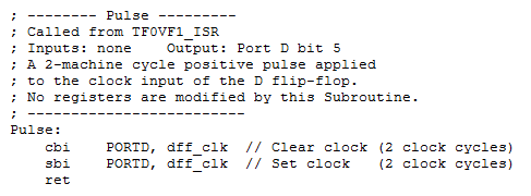
Next, add a call to the Pulse subroutine (rcall Pulse) after the call to Delay in the Main loop. Now let’s see if everything is working.
Green LED Test Sequence
When you press the reset button, the Green LED on your board should turn on for a short period of time before your program starts running at which time it should turn off. Try it now! If it does not momentarily turn ON, then most likely we are looking at a problem with the circuit.
No, Green LED does not turn on…
Open the detailed circuit schematic of the proto-shield. Using a digital multimeter verify that your 74ALS74 IC is getting five volts (pin 8 is GND and pin 14 Vcc).
IC is not getting Power
It the IC is not getting power trace back (see detailed schematic) to find what parts if any have power. From this information you can hopefully find out where the problem is. For example: power pin is not soldered. Next check if after reset the /Q1 output is high (pin 6).
IC is getting Power
If it is getting power you need to check if reset was applied. Using the multi-meter verify that the CLR input (pin 1 1CLR) to the 74ALS74 is swinging between 5v and 0v (approximately) when you push and release the reset button.
Reset (CLR input) is not toggling
It the CLR input is not being toggled, then trace back (see detailed schematic) to find out why button pin is not pulled up (resistor not wired correctly) or signal is not getting to the IC.
Yes, Green LED turns ON…
Once your program starts running the Green LED should turn off. If it does not then most likely Port D pin 5 is not being clocked. Did you remember to call pulse from your main loop? If pulse is being called correctly, then modify the pulse subroutine to toggle one of the discrete LEDs.
When you press the button the Green LED should turn ON, after a slight delay and then turn OFF when the button is released. A failure here most likely means that the button is not connected to the input of the flip-flop. Using your multimeter, verify at the input to the D flip-flop that when the button is pressed the voltage swings to 0 v.
External Interrupt Service Routine (ISR)
Section 11 “Interrupts” of the ATmega328P data sheet provides detailed instructions on how to configure the ATmega 328P processor to support external interrupts. We will be using External Interrupt Request 0 (INT0) to interrupt the processor whenever the user presses the button wired to our debounce circuit, the output of which is wired to Port D pin 2 (see proto-shield schematic).
Configure External Interrupt 0 registers EICRA and EIMSK
Let’s begin by looking at what the conditions need to be to trigger an external interrupt. Specifically, we need to tell the processor which external interrupt is enabled and if the interrupt is triggered based on the level or edge of the input signal. The ATmega 328P supports two external interrupts which are individually enabled by setting bits INT1 and INT0 in the External Interrupt Mask Register (Section 12.2.2 EIMSK).
For External Interrupt 0 bits ISC01 and ISC00 of the External Interrupt Control Register (Section 12.2.1 EICRA) determine if the interrupt is triggered based on the level or edge of the input as defined in Table 2 “Interrupt 0 Sense Control”.
We want to trigger our external interrupt on “The falling edge of INT0” so we want to set ISC01:ISC00 = 102 (the colon simple means these two bit together). Insert the following code in the reset section of your program to configure the External Interrupt Mask Register (EIMSK).

The location of this code snip-it is not important as long as it is in the reset (before loop label) section of your code. What is important is the location of the “Set the Global Interrupt” Flag (I) in SREG (Status Register) instruction (sei) . As a general rule, I enable interrupts (using instruction sei) as the very last step in the initialization process – just before the label loop. For example:
sei // Global Interrupt Enable
loop:
Add INT0 to Interrupt Vector Table
After enabling external interrupt zero (sbi EIMSK, INT0) and all interrupts (sei), if an interrupt is asserted on the INT0 line then the processor will automatically jump to location 0x0002 (INT0addr) in the Interrupt Vector Table (IVT) located in Flash Program memory. Before it jumps to this location it will also save the current location of the Program Counter (PC) so it can return to the interrupted program.
Add a jump to our INT0 Interrupt Service Routine at this location in the IVT.
RST_VECT:
rjmp reset

; ----- Interrupt Vector Table (IVT) -----

.ORG INT0addr // 0x0002 External Interrupt Request 0
 jmp INT0_ISR // Sect 4.7 Reset & Sect 9.4 Interrupt Vectors in ATmega328P

.ORG 0x0100 // bypass IVT
Table 11-6 “Reset and Interrupt Vectors in ATmega328P” provides a complete list of all 26 interrupts supported by our microcontroller. With respect to the above code, notice that our Interrupt Vector Table now implements one of these interrupts. At this time you may want to read the Owner’s Manual located near the end of the lab.
Write INT0 Interrupt Service Routine
As discussed in the Owner’s Manual we only want to display the room in the maze that the bear is entering after the button is pressed. We will implement this change by adding a third state (S2) to the FSM designed in part A of the lab. To transition to this third state, a new variable named walk will be set to true. Once defined and initialized, the ISR will set this variable.
Step 1: Add an assembly directive equating the text string “S2” to the number 0b10
.EQU S0 = 0b00 // state 0
.EQU S1 = 0b01 // state 1
.EQU S2 = 0b10 // state 2
Step 2: After this equate, add an assembly directive equating the text string “true” and “false” to 0xFF and 0X00 respectively.
; true and false
 .EQU true = 0xFF
 .EQU false = 0x00
Step 3: Define variable walk
 room: .BYTE 1
 dir: .BYTE 1
 next_state: .BYTE 1 // FSM next state
 walk: .BYTE 1
Step 4: Initialize the variable
 clr r16
 sts dir, r16
 sts room, r16
 sts next_state, r16
 sts walk, r16 // do not walk
Step 5: Add the following external interrupt service routine, which updates the variable room. Place just after the main loop.
 rjmp loop

 ; ---- External Interrupt 0 Service Routine -----------------
 ; Called when a falling edge is asserted on the INT0 pin (PIND2)
 ; INTF0 flag automatically cleared by AVR on vector interrupt
 ; SRAM Variable room is modified by this ISR
 INT0_ISR:

 push reg_F
 in reg_F,SREG
 push r16

 ldi r16, true
 sts walk, r16

 pop r16
 out SREG,reg_F
 pop reg_F
 reti
Software Implementation of a 3-State Finite State Machine
Now lets add a third state (S2) to the 2-state FSM built in the part A of the lab.
We have just written the ISR to set the variable walk to true when the user presses the programmable button on the protoshield. As seen in FSM state transition diagram above, when walk is true, we want to transition to our new S2 state. Within S2 we want to set the walk variable back to false, takeAStep, and display the room only.
Step 1: Move the code that assigns the switches to the room in the main loop to a new subroutine named takeAStep.
loop: call ReadSwitches // read switches into r7mov r17, switch // move switch (r7) to temporary register r16cbr r17, 0x0F // mask-out least significant nibbleswap r17 // swap nibblessts room, r17 // save formatted value to SRAM variable room// dir = switch & 0x03; mov r17, switch // move switch (r7) to temporary register r16 cbr r17, 0xFC // mask-out most significant 6 bits sts dir, r17 // save formatted value to SRAM variable dir. : rjmp loop : TakeAStep: push r17 call ReadSwitches // read switches into r7 mov r17, switch // move switch (r7) to temporary register r16 cbr r17, 0x0F // mask-out least significant nibble swap r17 // swap nibbles sts room, r17 // save formatted value to SRAM variable room pop r17 ret
Step 2: Update the next state decoder for state S1 to reflect the FSM
state_S1:

cpi r20, S1
 brne case_S2
 // output decoder
 :
 // next_state decoder
 lds r17, walk
 tst r17
 ldi r16, S0 // guess don't walk
 breq end_S1
 ldi r16, S2 // wrong guess, walk
 end_S1:
 sts next_state, r16
 rjmp end_switch // break
Step 3: Write your new S2 state.
state_S2:

cpi r20, S2 // test is optional for this lab
 brne end_switch
 // output decoder
 write the code to set walk to false, TakeAStep, and DrawRoom

// next_state decoder
 write the code to set next_state equal to S1
Lesson Learned
By Nicholas Lombardo (F’14)
I have helped several people with debugging and one thing that I saw repeatedly was people using “lds r16, false” when they should be using “ldi” since false is equated to a constant 0x00. I assume that what ends up happening is that the compiler loads the register at ext. I/O address 0x00 which, if I recall correctly, is r0.
It can be a little confusing the first time around, but using the bug usually manifests in the program looping between state 1 and state 2 and is very hard to catch unless you know what you’re looking for. The first time I helped someone with this, it took about an hour of scouring the code and back-stepping until we found out the fix which was literally changing a single letter.
Test Your Program
You may upload your program to quickly check to see if it works. An updated Owner’s Manual is provided in the next section to help you step through the maze. Follow the steps in the Owner’s Manual to check the operation of your program. I would be surprised if your program works the first time; if it does not, you will need to simulate the steps defined in the Owner’s Manual. See “Simulation and Debugging” for help here.
Owner’s Manual
Follow these steps to navigate a maze.
- Download and run the program. The bear should be shown at the entrance of the maze – an empty room. The direction you want the bear to walk should also be blinking. Specifically, toggle switches SW1 and SW0 to tell the bear to walk north. You will not be using switches SW3 or SW2 in this lab – set them both to 0 (no turn).
- Using the maze from Lab 1 as a guide and following the direction indicated by the seven segment display, input the next room the bear will be entering by toggling switches SW7 to SW4. The room LEDs on the 7-segment display should not be updated as you toggle the switches.
- Push the button to provide the bear with the directions. You should now see the room you entered in step 3 displayed along with the direction in which the bear was told to walk (note: the direction may not be visible if it is obscured by a wall).
- Toggle switches SW1 and SW0 to tell the bear which way to walk next. The blinking direction LED on the 7-segment display should be updated as you toggle the switches.
- Repeat steps 2 through 4 to verify the basic operation of the program. You do not need to guide the bear all the way to the forest.
Simulation and Debugging
Enter and verify the basic operation of the program using AVR Studio. Remember, before you run any program you should know what values will be contained in the effected registers. Tip: Within the simulation window expand the PortD, EXTERNAL_INTERRUPT, and TIMER_COUNTER_1 items in the I/O View window to easily initiate an interrupt and to view the operation of your program. To initiate an interrupt you can simulate the button being pushed by toggling PortD PIND bit 2.
- Stop program execution
 . In the I/O View window select PORTD. In the bottom window check PIND bit 2. This simulates pressing the button down.

- Single step the program
 once or twice. Then uncheck PIND bit 2. This simulates releasing the button. The external interrupt is configured to trigger on the falling edge of the input signal.

- Single step the program
 at least twice to initiate the call to the interrupt. You should now see the program counter go to the INT0 address (INT0addr) within the interrupt vector table (IVT).
Note: Unlike Timer Interrupts you cannot initiate an external interrupt by directly setting the external interrupt flag.
After you have verified the basic operation of your circuit, and your INT0 interrupt service routine (ISR), upload and run your program on the Arduino.
Lab Demonstration
You may be asked to…
- Simulate an external interrupt
- Demonstrate using AVR Studio that the SRAM variable room is updated every time the button is pressed.
- Demonstrate the correct operation of your program as defined in your “Owner’s Manual” found at the beginning of this lab.
Design Challenge – Timer 0 (4 Points)
You can skip these sections if you are happy receiving a passing grade (“C+”) on the lab. If you want to receive a good or excellent grade you will need to accept the challenge.
You may have already discovered that if you press the button quickly enough the new room is not updated. The cause of this intermittent behavior comes from the current design clocking the D flip-flop every 250 ms (4 Hz). To solve this problem, apply what you learned in Lab 4A and lecture to call the pulse subroutine every 10 msecs (100 Hz). This time is fast enough to catch the button being pressed, while also filtering out any switch bounce. There are two methods for implementing this, which are modifying the existing delay subroutine or to utilize the overflow interrupt.
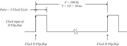
Here are some tips to help you translate your code from Lab 4A’s Timer 1 to Lab 4B’s Timer 0
Calculate Timer 0 Load Value
While Timer 1 is a 16-bit timer, Timer 0 is only an 8-bit timer. This introduces a number of problems. First, an 8-bit timer can not generate a 10 msec delay with the clock divided by 64. Fortunately, it can with the clock divided by 1024. Next, instead of subtracting by 216 = 65,536, you now will want to subtract by 28 = 256. Next, you will be reloading TCNT0, a single 8-bit register and not a 16-bit register (8 bit registers TCNT1H and TCNT1L).
Setup and Timer 0 Polling
Probably the most subtle difference between the two timers is the mapping of the registers. All Timer 1 Registers (TCCR1B, TCNT1H, TCNT1L, and TIMSKI) are outside the I/O address space of the ATmega 328P. Consequently, you used the Store to SRAM (sts) assembly instruction for accessing these registers. In contrast Timer 0 Registers TCCR0B and TCNT0 are within the I/O address space of the ATmega 328P, while TIMSK0 remains outside the I/O address space. The main consequence of this mapping is the need to use the I/O output (out) instruction, in place of the sts instruction when writing to registers TCCR0B and TCNT0.
Do not forget to remove your call to the pulse subroutine from the end of the main loop.
For the first method of modifying the existing delay subroutine, consider how the polling routines work. We still require the 250 msec delay for the transition between states in the main loop. During that time, the program is unable to check the status of Timer 0. It is not possible to call one polling routine during another. There will be some modification required to generate the 250 msec delay and call the pulse subroutine every 10 msec.
For the overflow interrupt method, determine the registers that need to be modified and figure out the additional code that needs to be added.
Lab 4 Deliverable(s)
STOP Read the Lab READ ME document contained in the Labs Folder. Be absolutely sure you have followed all instruction in the “Lab Formatting” section of this document. Points will be deducted if you do not follow these instructions. You have been warned.
Make sure your lab notebook is up to date. Follow the guidelines provided in the “Lab Notebook” section of the Lab READ ME document.
Make sure you have read and understand the “Plagiarism” section of the Lab READ ME document, especially if you are repeating the class.
All labs should represent your own work – DO NOT COPY.
Table of Contents
- Basic Lab
a. Main Program (Title Block, Initialization (setup), Main Loop (loop))
b. Interrupt service routine INT0_ISR
c. Subroutines (TakeAStep, Delay, and Pulse) in that order. - Design Challenge – if applicable
Pre-Lab 5: Add Bees to the Maze
Up to this point you have worked with an illustration of the maze. To describe a room you have had to manually enter the room number.
In this lab you will begin working with an encoded version of the maze located in a look-up table.
The green numbers across the top and right side of the encoded maze correspond to the columns and rows of the maze. Each entry in the table defines the room at that row and column address. The definition of the room, corresponds to the switch positions you have been manually entering up to this point in the course. For example; after taking his first step, the bear is in the room at column address 0016 and row address 1316. Looking at our maze (Figure 2), we see at these coordinates is a room with only a west facing wall. The Programmer’s Reference Card (see Figure 3), tells us that a room with only a west facing wall is encoded as 01002 = 0x04. Looking at the first entry in the last line of the table, we see our room encoded as 0x04.
Each entry in the maze only requires the least significant nibble (4 bits) of each byte in the table. In this table you will be updating the table to include the bees in the maze. For example, room 0x09 at coordinates row = 13, column = 3 has three 2 bees in it (see Figure 1). To include these bees in our table we would change the entry from 0x09 to 0x29.
You can find a text version of the maze with rooms named maze.inc here. Open this maze in notepad or AVR Studio and add the number of bees as defined in Figure 1.
For the following questions, refer to your textbook as well as lecture 13-1 on “Addressing Indirect.”
Question 1
The following code is used to initialize the Z pointer for indirect addressing:
ldi ZH, high(table<<1)
ldi ZL, low(table<<1)
- Why are two registers required to initialize the pointer to the correct address?
- If the address for the start of “table” is at 0x0A2C and the data that is saved at that flash address is 0x49 and 0x8A, what will the value in the Z register be (for ZH and ZL) after the two lines of code are executed? Explain.
- What does the expression table<<1 represent? Describe what action is taken or what it does with the example values from part b.
Question 2
table: .DB 0b01000001 0b01100000 0b00100011 0b00000001
After initializing the z pointer to the start of “table,” the following code is executed:
clr r1
add ZL, r0
adc ZH, r1
lpm r16, Z
- If the value in r0 is 0x03, and the beginning address for “table” is 0x00D7, what is the value that is in ZH and ZL?
- According to the code above, where is the data being loaded to (the destination for the data) in the lpm instruction?
What Should I Turn In?
Turn in the following material two pages.
Page
- Title page with the pre-lab number, your name and picture, today’s date, and the day your lab meets.
- Your Maze.inc file with modified cells highlighted.
- Problem statements and answers for questions 1 and 2.
Lab 5A: Take a Step and Enter a Room/ Indirect Addressing Mode
At present, you enter the room by hand (SW7 to SW4). In this lab you will write subroutines to teach your bear how to take a step and enter a room. To accomplish your task this lab includes a digital description of the maze. No more room switches!
FUTURE ALERT!
In the PreLab for Lab 06 you will be translating your flowchart from PreLab 1 into an assembly program. If you were asked to plot a new path through the maze, be sure and receive the instructor’s approval before doing the PreLab. If you are not sure, you are responsible for asking.
If you decide to work on the “Congratulatory Tune” section of the Bonus Lab for Lab 6, you will need to purchase an inexpensive speaker and a carbon film resistor, 270 ohms at 250 mW. You will be wiring the circuit as drawn in the Arduino Proto-Shield schematic.
Table of Contents
What is New?
Here are some of the new concepts you will be exploring in this lab.
- Working with the Indirect Addressing Mode
The indirect addressing mode instruction lpm is introduced in this lab.
Create the Lab05 Project
If you are using a lab computer I would recommend erasing everything in Drive D and using this area for our project. Do not forget to save often. At the end of the lab do not forget to save to your Flash drive.
- Open AVR Studio and create a new Project named Lab05 (see Lab 1 for detailed instructions)
- Copy over maze.inc, pseudo_instr.inc, spi_shield.inc, testbench.inc, and upload.bat from Lab 5.
- Open the upload.bat file in notepad (right-click edit) and change the file name from Lab04.hex to Lab05.hex
- Copy the text in Lab04.asm into Lab05.asm
- Update the information in the title block.
- Build your project and verify you are starting with zero errors and zero warnings.
Cleanup
Before we begin, lets do a little more house cleaning. The items preceded by an empty box ☐ are probably not done and you will need to take some action. The items preceded by a checked box most likely have been completed, but you should double check to avoid debugging your program.
☐ The SRAM variable dir should be initialized so the bear is facing North (dir = 0x03).
☐ Verify that SRAM variable room is initialized so the bear is in an empty room (room = 0x00).
☐ Verify that SRAM variable next_state is initialized to state S0 (next_state = 0x00)
Take a Step and Enter the Room
As mentioned in the introduction, you currently enter a room within the maze by hand (SW7 to SW4). In this lab you will rewrite subroutine TakeAStep and write a new subroutine named EnterRoom to navigate a digital version of the maze (maze.inc). No more room switches! To see how this will work open the Lab05A Arduino Sketch within the Arduino IDE, and follow the steps defined in the “Updated Owner’s Manual” located near the end of this lab.
Add the following code to the output decoder section of state S2.
loop:
:
case_S2:
cpi r20, S2 // test is optional
brne end_switch
// output decoder
:
lds r20, dir // input arguments are dir, col and row
lds r22, col
lds r24, row
rcall TakeAStep
sts col, r22 // update column and row
sts row, r24
rcall EnterRoom // inputs to EnterRoom are outputs from TakeAStep
mov r22, r24 // save a copy of # of bees in the room
cbr r24, 0xF0 // remove the # of bees from the room
sts room, r24 // save the room number
swap r22 // swap # of bees to the least significant nibble
cbr r22, 0xF0 // remove the room from the # of bees
sts bees, r22 // save number of # of bees in the room
Notice that the new code incorporates your original call to TakeAStep included in the output decoder section of state S2. This original version simply read switch values SW7 – SW4 and placed them in variable room. In this lab the subroutines TakeAStep and EnterRoom perform the same function, without the switches. Here is what is happening in the code you just added; TakeAStep takes as input arguments row, col, and dir and computes the coordinates of the room the bear is entering. Consequently, it outputs the row and col address of this new room. EnterRoom takes these coordinates (row, col) as input arguments (r24, r22), computes an address within the encoded maze (maze.inc) and returns the room and bees at this address (r24 = bees:room).
The program then isolates the room from the bees and saves both into their respective variables (room and bees).
Once again notice that to maintain C++ compliance, arguments are sent in registers r24, r22, and r20. Function return values (bees:room) are contained in registers r24.
If you were to assemble your program now, you would receive a large number of errors, as the assembler looks for variables and a subroutine that is not there. We will be defining those variables at the beginning of the next section and writing the missing subroutine (EnterRoom) shortly.
Take a Step
Before we rewrite TakeAStep define three new SRAM variables to hold our current location (row and col) in the maze and the number of bees in a room.
.DSEG
room: .BYTE 1
dir: .BYTE 1
next_state: .BYTE 1 // FSM next state
walk: .BYTE 1
row: .BYTE 1 // the bear is in the room at this row
col: .BYTE 1 // and column address
bees: .BYTE 1
It is good programming style to always initialize variables as soon as you define them. At the beginning of the maze we want the bear located in row = 0x14 and col = 0x00. In the reset section of your program initialize SRAM variables row and col to these values. Next, initialize variable bees = 0 indicating that the bear has not yet encountered any bees. Do not forget to comment your code.
Now, write a subroutine to modify these variables containing the bear’s current room location (row and col) based on the direction you want the bear to walk. Specifically, translate the following truth table into assembly code. You may use any technique you like.
| dir | row | col | Comment |
| 00 | + | take a step South by incrementing the row | |
| 01 | + | take a step East by incrementing the column | |
| 10 | – | take a step West by incrementing the column | |
| 11 | – | take a step North by decrementing the row |
Do not forget to add your own comments to your code.
; —— Take A Step ——
; Called from INT0_ISR and main loop for animated version
; input r24, r22, r20 = row, col, dir
; output r24, r22 = row, col
; No other registers are modified by this subroutine.
; note: This simplified version can walk through walls
; ————————-
TakeAStep:
; push registers modified by your subroutine
; based on direction (r20) incr/decr row/col as defined in Table 5.1
; pop registers modified by your subroutine
ret
The simplest solution conceptually would be to implement a high level language if-then-else construct in assembly using cpi and brne, or bst and brts instructions. For additional assistance review your Lab03A code (TurnLeft, TurnRight, WhichWay).
Creative Corner – TakeAStep using Indirect Addressing Mode
The indirect addressing mode is the most elegant, the most difficult to understand, and of course, the method I used to program the TakeAStep subroutine. The lookup table solution shown in the Arduino Sketch Lab05A, would be implemented in assembly using the lpm instruction. My AVR Studio version of Lab05A uses the ijmp instruction. Please remember to indicate on the cover sheet of your lab report if you implemented this Creative Corner version of the subroutine.
Define the Maze
Before we can enter a room we must define all the rooms in the maze. Here you will use the maze you created in Prelab 5 (if you did not complete the prelab, you can find the maze without the bees here). Move your maze.inc file into the Lab05 project folder.
Open the maze.inc file you created in the pre-lab (File > Open File…).
Unlike Figure 2, your version should include the bees in the maze. Before we continue, let’s review how the maze is constructed (prelab 05). As you can see in Figure 2, I have organized the rows and columns of the table to match our maze (Figure 1). Each entry in the table defines the room and bees at that row and column address. The definition of the room corresponds to the switch positions you have been manually entering up to this point in the course. For example; after taking his first step, the bear is in the room at column address 0016 and row address 1316. Looking at our maze (Figure 1), we see at these coordinates is a room with only a west facing wall. The Programmer’s Reference Card (see Figure 3), tells us that a room with only a west facing wall is encoded as 01002 = 0x04. Looking at the first entry in the last line of the table, we see our room encoded as 0x04.
Include your definition of the maze by adding the following include assembly directive to your program.
.ORG 0x0100 // bypass IVT
.INCLUDE “spi_shield.inc”
.INCLUDE “testbench.inc” // DrawRoom and DrawDirection
.INCLUDE “maze.inc”
reset:
Enter the Room
Now that our bear has taken a step and we have our maze encoded, it is time to write the EnterRoom subroutine. The TakeAStep subroutine has already updated variables row and col to correspond to the coordinates of room we are currently in, so now all we have to do is translate that information into the a byte index into table theMaze. With a sharp pencil (or your smart device) and a little math you will discover that the byte index of a room as a function of the row and column is given by the equation 20 x row + col.
Do not forget to add your own comments. Please, do not copy and paste my explanatory text.
; ————————–
; —— Enter a Room ——
; Called from main program
; input r22, r24 = col, row
; output r24 = bees:room
; no other registers are modified by this subroutine.
EnterRoom:
; Push registers modified by your subroutine, including ZH and ZL.
; Do not push registers used to return values r24 and r22.
Write the code to save registers here
// Step 1: Base Address
ldi ZL,low(theMaze<<1) // load base address of theMaze into Z.
ldi ZH,high(theMaze<<1)
// Step 2: Calculate Byte Index
Using instructions mul, add, and adc, compute the index of the room by writing the code to implement equation 2010*row+col here. Be careful this is a 16-bit number so you need to add the carry (adc) into the most significant byte. To add only the carry, set a scratch register to zero (clr r2) and add it along with the carry (adc r1, r2).
// Step 3: Add Index to the Base Address and Load Room with Bees
Add the 16-bit index to the base address of theMaze by writing the code to implement equation ZH:ZL = ZH:ZL + r1:r0 here. Again, you will need to use both the add and adc instruction to add these two 16-bit numbers together.
; load the room and bees from program memory using the indirect addressing mode.
lpm r24,Z // load the room with # of bees indirect
; pop registers modified by your subroutine, including ZL and ZH
Write the code to pop the registers here.
ret
Test Your Program
You may upload your program to quickly check to see if it works. An updated owner’s manual is provided in the next section to help you step through the maze. I would be surprised if your program works the first time in which case you will need to simulate the steps defined in the owner’s manual. See “Simulation and Debugging” for help here.
Updated Owner’s Manual
Open the Lab05A Arduino Sketch within the Arduino IDE, and follow these steps to see how your program should navigate the maze.
- After you upload and run the program, no room should be displayed (the bear is outside the maze). Place both direction switches up, all other switches should be in the down (off) position.
- The North direction 7-segment LED should be blinking telling the bear to walk North.

- Push the button telling the bear to take a step. The bear should now be shown in the first room – a room with a west facing wall.
- Point the bear in the direction you want him to proceed by setting the direction switches.
- Push the button to provide the bear with the direction you wish him to walk. The bear now takes a step (TakeAStep) and enters the next room (EnterRoom) as defined by your encoded maze (maze.inc) file. You should now see the room displayed along with the direction in which the bear was told to walk (note: the direction may not be visible if it is obscured by a wall).
- Repeat steps 4 and 5 to verify the basic operation of the program. You do not need to guide the bear all the way to the forest.
Simulation and Debugging
Set a break point at your call to ![]() ReadSwitches and at the beginning of the
ReadSwitches and at the beginning of the ![]() INTO_ISR. Run
INTO_ISR. Run ![]() to the first break point and set direction switches so the bear is facing north, we no longer use the room switches.
to the first break point and set direction switches so the bear is facing north, we no longer use the room switches.

Step over ![]() the ReadSwitches subroutine. Register R06 should be equal to three (0x03). Initiate an external interrupt by toggling PIND bit 2 as described in Lab and duplicated here.
the ReadSwitches subroutine. Register R06 should be equal to three (0x03). Initiate an external interrupt by toggling PIND bit 2 as described in Lab and duplicated here.
- Check PIND bit 2

- Take at least two steps 2x
 . The check mark may disappear after the first step, this is due to the simulation of an internal synchronization circuit. It should reappear after the second step.
 - Uncheck PIND bit 2.

- Single step the program
 . You should within a few steps find yourself in the interrupt vector table (IVT). Take the jump into the INT0_ISR. Set a breakpoint or step to your call to TakeAStep. SRAM variable row and register R24 should equal 0x14 (decimal 20) and variable col and register R22 should equal 0x00. The direction and register r20 should be three (0x03).
 - Step over
 TakeAStep. You have just told the bear to take a step in the North direction, so register R24 = 0x13 and R22 = 0x00. If they are not, then you should repeat steps 1 to 3 and this time step into
  TakeAStep and locate the bug.
 - Step to and over
 EnterRoom. The bear should now have entered the first room, one with a west facing wall, which means register R24 = 0x04. If the bear is not in this room, then you should repeat steps 1 to 4 and this time step into
  EnterRoom and locate the bug.
Review the “Define the Maze” Section of this lab if you are not sure why R24 should equal 0x04. - Congratulations, your bear has now taken his first step and entered the maze. You now can upload your program and manually walk the bear around the maze. If you run into a bug along the way you should return to the simulator and manually enter the row and column just before the bug was discovered on the board and then repeat steps 1 to 5 having the bear enter the problematic room.
Design Challenge A – Room with Bees (1 – 3 points)
This is the first of two design challenges. You can skip these sections if you are happy receiving a passing grade (“C”) on the lab. If you want to receive an good or excellent grade you will need to accept one or more of the challenges.
In the Pre-Lab you encoded the number of bees in the room. Modify your program so as the bear walks into a room with bees, the number of bees in the room is displayed on the seven segment display for at least half a second (500 ms). After this delay the room is again displayed. This modification should not affect the performance of the rest of the lab.
Lab Demonstration
You may be asked to…
- Simulate an external interrupt
- Demonstrate using AVR Studio that the SRAM variable room is updated every time the button is pressed.
- Demonstrate the correct operation of your program as defined in your “Owner’s Manual” found at the beginning of this lab.
Make a backup copy of your project folder before moving to Lab 05B
Lab 5B: A Little Animation
Is your finger tired from pushing the button every time you want the bear to take a step? In this last part of lab 5, you are going to teach your bear how to walk down a hallway by himself to speed up his navigation through the maze.
Table of Contents
What is New?
Here are some of the new concepts you will be exploring in this lab.
- Implementing Logical Operators (&&, ||) in Assembly
- 4-State Finite State Machine (FSM)
No new assembly directives or instructions are introduced in this lab.
Part I – IsHallway
What Question Does IsHallway Answer?
In the second part of this lab you are going to teach the bear how to walk down a hallway until he encounters bees, a corner, or an intersection. Clearly, before you can tell the bear to walk down a hallway, you need to test for these conditions – is the bear in a hallway without any bees? To help answer that question, you are going to write a new function named IsHallway.
The hallway question is answered by looking at Figure 1 Programmer’s Reference Card. Here we see that Room 6 (room = 01102) is a vertical hallway and Room 9 (room = 10012) is a horizontal hallway. If room equals either of these two values (it is a hallway) and the hallway does not contain any bees, then your function will return a non-zero value (true), otherwise the function will return zero (false).
The bee question will be answered by testing if r22 (bees) is equal to zero (tst).
Arduino C++ IsHallway
In the previous section I described how IsHallway works in words. A more concise answer is provided by simply looking at the C++ code which does the equivalent operation. If you open the Arduino script Lab05B.ino you will see IsHallway defined as…
boolean isHallway(byte room, byte bees){
return (bees == 0x00 && (room == 0x09 || room == 0x06))
}
IsHallway Returns a Boolean Answer in r24
As you have learned in past labs, functions return values in the r24 register. Following this convention allows your functions to be called from C++ and assembly. For these functions you did not push/pop r24 allowing the register to provide the answer to the question asked (ex. did your right paw touch a wall?). If your function, like IsHallway, returns a Boolean value (true or false) then the calling program immediately executes a tst instruction followed by a breq (answer is false) or brne (answer is true) instruction. The branch selected is based on the program path you wish to take.
Use the comments in the following IsHallway template to complete your new function. Do not forget to add your own comments.
; ————————–
; — Is this a Hallway? —
; input r24 = current room (room), r22 = bees
; output r24 = 0 if answer is false (r24 == 0),
; otherwise the answer is true (r24 != 0).
; The answer is true if the bear is in a hallway
; without any bees.
; no registers are modified by this subroutine
; ————————-
IsHallway:
// return (bees == 0x00 && (room == 0x09 || room == 0x06));
1. Test (tst) if the room has bees R22 != 0x00. If the answer is yes (brne), go to answer_is_no.
2. Compare (cpi) room to a horizontal hallway (room == 0x09). If the answer is yes (breq), go to answer_is_yes
3. Compare (cpi) room to a vertical hallway (room == 0x06). If the answer is yes (breq), go to answer_is_yes
answer_is_no:
ldi r24, false // room is not a hallway or contains bees
rjmp endOfHallway
answer_is_yes:
ldi r24, true
endOfHallway:
ret
Test IsHallWay
Here is a subroutine to test your new IsHallWay function named TestIsHallway. To display the answer, TestIsHallway uses discrete LEDs 5 and 4 as shown in Figure 2.
; ————————–
; —– Test IsHallway —–
; Called from LED display section in the main loop
; Input: r24 Outputs: spiLEDs bits 5 and 4 only
TestIsHallWay:
push r16
mov r16, spiLEDS
tst r24 // test return value from isHallway
brne inHallway
sbr r16, 0b00010000 // Bear is not in hallway, so turn on LED 4
cbr r16, 0b00100000
rjmp doneHallway
inHallway:
sbr r16, 0b00100000 //Bear is in hallway, so turn on LED 5
cbr r16, 0b00010000
doneHallway:
mov spiLEDS, r16
pop r16
ret
Place TestIsHallway in the Test Subroutines section of your program, which is after the main loop.
Add calls to your new IsHallWay and my TestIsHallway procedures in your discrete LED display area of the main loop.
/* Update Discrete Red LEDs */
:
lds r22, bees
lds r24, room
rcall IsHallWay
rcall TestIsHallway
rcall Delay
rcall Pulse
// writeDisplay(leds,seg7);
call WriteDisplay
rjmp loop
Before proceeding to the next section, upload your program and test your IsHallWay function to make sure the bear knows when he is in a hallway (LED 5 is ON) or not (LED 4 is ON), or if he sees any bees (LED 4 is ON).
You will be adding IsHallWay in the next section as part of your Finite State Machine (FSM). Now that you have tested your IsHallway subroutine you may delete this section of code or keep it to provide additional insight into the operation of your FSM.
Part II – A little Animation
If the bear is in a hallway we want him to walk down the hallway. Specifically we want him to mimic the user pressing the button.
Software Implementation of a 4-State Finite State Machine
To teach our bear to walk down a hallway, we will be adding a fourth state to our FSM as described in Figure 3.
In Lab 4 Part A “Software Implementation of a 2-State Finite State Machine” you built your first FSM. In Lab 4 Part B “Software Implementation of a 3-State Finite State Machine” you extended your design to include a third state. Applying what you learned in Lab 4, add a 4th state as defined by Figure 3 “4-State Moore Finite State Machine (FSM).” As always if you need additional help you can look at the Arduino Script version of the lab (Lab05B.ino). That’s it! Have fun helping your bear solve the maze. That is of course after you have debugged the program.
The hallway variable that is present in Figure 3 is referring to the output from the IsHallway subroutine. Use the diagram to figure out where in the code you will need to call IsHallway and how that will be utilized in the next_state decoders. Remember, you cannot go directly to another state and must update the next_state variable with the correct value.
Test Your Program
You may upload your program to quickly check to see if it works. An updated owner’s manual is provided in the next section to help you step through the maze. I would be surprised if your program works the first time in which case you will need to simulate the steps defined in the owner’s manual. See “Simulation and Debugging” for help here.
On a personal note, when I wrote this program for the first time, I do not know how many hours it would have taken to get it working without the simulator.
Updated Owner’s Manual
Follow these steps to navigate a maze. You can follow along by opening Lab05B.ino within the Arduino IDE.
- After you upload and run the program, no room should be displayed (the bear is outside the maze). Place both direction switches up, all other switches should be in the down (off) position.

- The North direction 7-segment LED should be blinking telling the bear to walk North.
- Push the button telling the bear to take a step. The bear should now be shown in the first room – a room with a west facing wall.
- Point the bear in the direction you want him to proceed by setting the direction switches.
- Push the button to provide the bear with the directions. You should now see the bear walk (hallway blinks on and then off) until a decision needs to be made (a corner, fork in the road, or bees). The room the bear is in along with the direction (blinking) in which the bear was told to walk should now be displayed.
- Repeat steps 4 and 5 until the bear makes it to the forest.
Simulation and Debugging
You have added a lot of code to your program and the probability that it will work the first time you upload it are not good. Consequently, you will need to use the simulator to find the problem.
Here you will use the techniques learned in previous labs to set timer and external interrupts. In addition I would recommend using the watch window to quickly update and track your variables.
If it is not already open from the menu bar select View and Watch. Now left click the variables you want to update and track and select and from the pop-up menu select
Add Watch: “some variable”
When I was debugging my program I watched variables row, col, blink, state, and room. Here is what their values are after initialization.
Erratum: The original form of the state variable, was a variable named blink. It is this variable that is shown in the screen capture here and in subsequent screen captures.
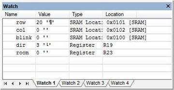
As you can see the bear is standing just outside the maze (row = 20 col = 0) facing north (dir = 3) in an empty room (room = 0). All numbers are in decimal so you may want to convert to hexadecimal.
Instead of spending time walking your bear to a location that includes a bug, you can now simply modify the variable in the watch window to take your bear directly to the problem. In this sample watch window I have positioned my bear in the first hallway.

Here are two watch windows testing the first instance of the bear entering a room with bees. The two cases are testing the effect of variable blink on this room.
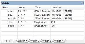
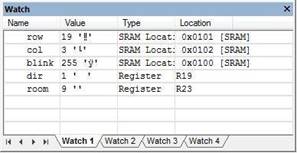
In this final example, my bear is entering the third left hand turn of the shortest path.
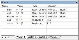
Design Challenge B – Walk into a Wall (2 points)
This is the second of two design challenges. You can skip these sections if you are happy receiving a passing grade (“C”) on the lab. If you want to receive a good or excellent grade you will need to accept one or more of the challenges.
Modify TakeAStep to not take a step and to set the four remaining LEDs (3 to 0) if the bear walked into a wall.
Lab 5 Deliverable(s)
STOP Read the Lab READ ME document contained in the Labs Folder. Be absolutely sure you have followed all instruction in the “Lab Formatting” section of this document. Points will be deducted if you do not follow these instructions. You have been warned (again, and again and again…)
Make sure your lab notebook is up to date. Follow the guidelines provided in the “Lab Notebook” section of the Lab READ ME document.
Make sure you have read and understand the “Plagiarism” section of the Lab READ ME document, especially if you are repeating the class.
All labs should represent your own work – DO NOT COPY.
Pre-Lab 6: Teaching the Bear to Navigate the Maze
Part 1 – Stack Initialization
The stack pointer of the AVR processor is always pointing to the next available location in SRAM to store temporary data. In Lab 2, I moved the stack pointer to the top of memory with the following code snip-it.
ldi r16,low(RAMEND) // RAMEND address 0x08ff
out SPL,r16 // stack Pointer Low SPL at i/o address 0x3d
ldi r16,high(RAMEND)
out SPH,r16 // stack Pointer High SPH at i/o address 0x3e
As your code becomes more complex, the possibility of losing control of the stack becomes a very real possibility, resulting in a stack underflow or overflow condition.
Question 1 What is stack underflow and overflow?
Question 2 In Lab 3A Appendix A Rules for Working with Subroutines, I gave you a few rules to remember when writing your main program and subroutines, which of these rules, if not followed, would result in a stack underflow and/or overflow condition. Explain your answers.
Part 2 – Translating your flowchart from PreLab 1 into an assembly program
Question 3 One of the lab objectives is to see if the bear is in the forest (i.e., home). Your code will accomplish this by checking the row the bear is currently in. The rows and columns of the maze are numbered from 0 to 19 (0x13) starting in the upper left hand corner. When the bear has found his way out of the maze he is in row minus one (row < 0). How would you represent minus 1 in hexadecimal using 2’s complement notation?
Question 4 Translate your flowchart from PreLab 1 into an assembly program. If you were asked to plot a new path through the maze, and have not done so, please see me (lab instructor) as soon as possible. Note that if your path does not go through the target square corresponding to the last four digits of your student ID, you will receive a zero for lab 6. If you are not sure, you are responsible for asking.
In PreLab 1 you designed a flowchart for the WhichWay routine. This flowchart from PreLab 1 used subroutine names for sensor (used in a conditional expression) instructions Hitwall, RightPaw, and LeftPaw and actuator (take some action) instructions TurnLeft, TurnRight, TurnAround, InForest and CountBees. By the end of lab 3 most of these were no longer names, but working assembly subroutines. Working from your PreLab 1 flowchart, and incorporating calls to these subroutines, write an assembly program to implement the flowchart.
For help read Lab 6A which shows you how to translate the shortest path flowchart into an assembly program.
What Should I Turn In?
Turn in the following material three pages. Make sure all your original work is in your Lab Notebook. All written material must be typed or very neatly done in ink. Once again please do not copy.
Page
- Title page with the pre-lab number, your name, today’s date, and the day your lab meets.
- Answers to the four questions. Do not forget to summarize the question and highlight your answers.
- Your approved flowchart from Prelab 1.
- Your WhichWay subroutine. This may be done in AVR Studio (recommended).
Lab 6A: aMazing Solution/ WhichWay
Lab 6 is worth 30 points. Shortest Path is worth 10 points, Your Path is worth 10 points, In Forest (Lab 6B) is 5 points, and Count Bees (Lab6B) is 5 points.
The WhichWay subroutine that was written for Lab 3 tells the bear which way to go by setting switch positions SW1 and SW0 for the direction and SW3 and SW2 for which way to turn. We will now be updating it to navigate through the maze using the logic developed in Prelab 1.
In this lab, you will first create an assembly version of the shortest path solution called ShortWhichWay with. Next, you will implement the flowchart you wrote in PreLab 1 and translated into assembly code as part of PreLab 6.
When you are done teaching the bear how to get out of the maze by himself, you will no longer need any of the eight switches as inputs. No more switches!
Table of Contents
What is New?
Here are some of the new concepts you will be exploring in this lab.
- Translating a flow chart and high-level code into assembly.
No new assembly directives or instructions are introduced in this lab.
Create the Lab 6 Project
If you are using a lab computer, I would recommend saving all of your files to a flash drive. Do not forget to save often. At the end of the lab, do not forget to save the latest version and take your flash drive with you.
- Open AVR Studio and create a new Project named Lab06 (see Lab 1 for detailed instructions)
- Copy over maze.inc, pseudo_instr.inc, spi_shield.inc, testbench.inc, and upload.bat from Lab 5.
- Open the upload.bat text file in notepad (right-click edit) and change the filename from Lab05.hex to Lab06.hex
- Copy the text in Lab05.asm into Lab06.asm
- Update the information in the title block.
- Build your project and verify you are starting with zero errors and zero warnings.
Before You Start
Verify that SRAM variable dir is initialized so the bear is facing North (dir = 0x03).
Verify that SRAM variable room is initialized so the bear is in an empty room (room = 0x00).
Verify that SRAM variable next_state is initialized to S0 (next_state = 0x00).
Verify that SRAM variable row is initialized to the starting location just outside of the maze. (row = 0x14).
Verify that SRAM variable col is initialized to the starting location (col = 0x00).
Verify that SRAM variable walk is initialized so the bear does not automatically take a step. (walk = 0x00).
A Little House Cleaning
Open the pseudo_instr.inc include file in AVR Studio. You need to Build your project (step 6 in “Create the Lab 6 Project” for the include files to be shown in the Project window.
Move the subroutines TakeAStep, EnterRoom, and IsHallway created in Lab 5 from the Lab6.asm main application to the pseudo_instr include file. Optionally, you may delete TestIsHallway or also move it to the pseudo_instr include file. You may notice that in the figure it shows Lab6A not Lab6.asm. I created a new project for each part of a lab. This allows me to easily move from one to the other. You have the option of simply making a copy of your labs so that you can step back in time.
At this time, the main application Lab6.asm should only have the initialization (reset), main loop (loop), the interrupt service routine (INT0_ISR) and the subroutines Delay and Pulse. All other subroutines should be located in include files or deleted. Any subroutines created for design challenges should also be moved to the include files.
Part I – Shortest Path
Before you implement your solution, let’s verify that your nearly complete program is working by implementing the shortest path (fewest bees) solution to the maze.
Step-by-Step Solution
- Remove the code that updates the variable dir based on switch positions from the main program. In the main program, you read the switches and set variable dir. You no longer use the switches on the shield to set dir, or anything else for that matter, so delete this section of your program.

- Add a call to a to-be-written ShortWhichWay subroutine. Place the subroutine call after the bear takes a step and enters a room (State S2). As shown here, the direction variable dir is updated after each call to ShortWhichWay.

- Copy and Paste my ShortWhichWay subroutine which implements the shortest path solution. I have superimposed the Arduino version of the WhichWay subroutine from Lab06A.ino so you can compare the two implementations.
; — Which Way Do I Go? —
; Called from main program
; Input: r24 = direction, r22 = room
; Output: r24 = direction
; No registers or flags are modified by this subroutine
ShortWhichWay:
mov r17, r24 // save to temporary register
// if(!rightPaw(dir, room))
rcall RightPaw // r22 = room, r24 = dir
tst r24
brne else_if_hitwall
// dir = turnRight(dir);
mov r24, r17 // move direction to calling argument
rcall TurnRight // new direction now in r24
rjmp which_end
// else if (hitWall(dir, room))
else_if_hitwall:
mov r24, r17
rcall HitWall // r22 = room, r24 = dir
tst r24
breq else
// dir = turnLeft(dir);
mov r24, r17
rcall TurnLeft // new direction now in r24
rjmp which_end
else:
mov r24, r17 // do not change direction
which_end:
ret
Assemble and upload your new program. If everything is working, your bear should now be able to navigate his way out of the maze, encountering the fewest number of bees. You should only need to push the step button when a decision needs to be made (corner, intersection, or encounters bees). And the really good news is you no longer need to toggle any switches!
Test Your Program
You may upload your program to quickly check to see if it works. An updated owner’s manual is provided in the next section to help you step through the maze. I would be surprised if your program works the first time in which case you will need to simulate the steps defined in the owner’s manual. See “Simulation and Debugging” for help here.
Updated Owner’s Manual
Follow these steps to navigate a maze.
- Download and run the program. The bear should be shown at the entrance of the maze – an empty room. The north facing direction 7-segment LED should be blinking instructing the bear to walk north. Toggling the switches should have no effect.

- Push the button to provide the bear with the directions. You should now see the room you entered displayed along with the direction in which the bear should now proceed.
- Repeat step 2 until the bear makes it to the forest.
- Push the button telling the bear to take a step. The bear should now be shown in the first room – a room with a west facing wall. You should also see the direction in which the bear should now proceed as defined by your WhichWay subroutine.
- Push the button to provide the bear with the direction. You should now see the bear walk (hallway blinks on and then off) until a decision needs to be made (a corner, fork in the road, or bees). The room the bear is in along with the new direction (blinking) in which the bear is facing, as defined by your WhichWay subroutine, should now be displayed.
- Repeat steps 5 until the bear makes it to the forest. What should be displayed on the seven segment display when the bear enters the forest is for now, undefined, so anything displayed is okay.
Simulation and Debugging
If your program does not work, then of course you will need to use AVR Studio’s simulator/debugger.
To faithfully simulate your program you will need to manually set the timer flag and trigger an external (button) interrupt as your bear travels the maze. If your bear gets confused fairly deep into the maze then set the row and column a few steps before the problem area and then set the timer flag and trigger an external (button) interrupt for the few steps needed for him to encounter the problem.
Don’t forget these helpful tips. You can right-click any variable and add it to the watch window. If the watch window does not already show values in hexadecimal, right click inside the window and select “Display all Values as Hex.”

Part II – My aMazing Solution
Replace the shortest path solution to the maze with the path defined by your flowchart from PreLab 1 as implemented by your WhichWay assembly subroutine written in PreLab 6. Rename that subroutine to be MyWhichWay in order to avoid any confusion over which version of WhichWay you are calling (from lab 3, the shortest path, from prelab 6).
This portion of the lab is not optional!
A Bug Story
Like you, I downloaded my program hoping it would work immediately and of course it did not. The direction segment stayed pointing North and a closed room appeared on the second step. My first course of action was to simplify, so I commented out most (I thought I had commented out all) of the new code and replaced it with the original WhichWay code. I then uploaded my simplified program and the problem did not go away. I suspected I had somehow broken the original version; but how? After simulating my call to WhichWay I rediscovered that the part of the code that called WhichWay saved the new direction returned in r24 to variable dir. I thought the new WhichWay did this step. Going back to WhichWay I discovered that I had not commented out a new section where I added push and pop r24 instructions to make my subroutine more transparent. Instead it broke the program. I removed the push/pop and my bear was on his way again.
Lab 6B: aMazing Solution/ Welcome Home
Your bear can now navigate the maze by himself. In this part of the lab, you will complete the Main loop routine by checking to see if the bear is in the forest. Plus, wouldn’t it be nice to welcome your bear home by reporting how many bees he encountered along the way or better yet play a song. In this second part of the lab and the bonus lab you will get the opportunity to do all this and more!
If you test drive the Lab06B.ino program you will see that it displays the number of bees along the way. This was a Lab 6 design challenge and is not a required part of Lab 6B. If you have not yet implemented this feature you can add it as part of the bonus lab.
Table of Contents
What is New?
Here are some of the new concepts you will be exploring in this lab.
- How to test and branch for the opposite sense of conditional expression
- How to put a Microcontroller to Sleep
No new assembly directives or instructions are introduced in this lab.
Update State_S2
Add the following comment blocks to the output decoder section of State S2. These are the two sections you will write in this lab. You are going to be responsible for adding the code at the correct location.
state_S2:
cpi r19, S2
brne end_switch
/* Output Decoder */
/*
* step
* 1 check to see if the bear is in the forest.
* if the answer is yes, welcome the bear home.
* 2 check to see if there are any bees in the room
* if the answer is yes, count the number of bees
*/
Part I – In the Forest
Test (tst) the Row
In this part of the lab, you will write the code to see if the bear is in the forest (i.e., home) and learn more about conditional branching. Your code accomplishes this by checking the row the bear is currently in. The rows and columns of the maze are numbered from 0 to 19 (0x13) starting in the upper left hand corner. When the bear has found his way out of the maze he is in row minus one (r24 < 0). When this occurs, your code should call the subroutine InForest. You can also see how I wrote the equivalent test in C++ by opening the lab06B.ino program within the Arduino IDE.
As shown in Figure 1 and in the Lab06B.ino program C++ example, the code to check to see if the bear is in the forest is placed after TakeAStep and before EnterRoom. This code placement makes sense, given that if the bear is in the forest, there is no room to enter! If the bear is in the forest, call the to-be-written subroutine InForest.
Use the test instruction (tst) to find out if the value in a register is less than or greater than zero. Choose the corresponding branch instruction that will make this conditional check work as intended. For example, brne will not work because positive values will also cause it to trigger. If you would like additional help in writing the test to check to see if the bear is in the room see Appendix A, specifically the discussion on the test instruction.
InForest Subroutine
When the bear has left the maze and is now in the forest (i.e., home), call the following InForest subroutine. The InForest subroutine, when called, displays a 0 on the 7 segment display and clears the discrete LEDs. It then turns off the timer and disables the external interrupt. Once the forest is entered, the only way to restart the program is to press the reset button.
; ————————–
; ——- InForest ———
; Input: none Outputs: none
; Warning: Subroutine enters power down mode.
; Press reset button to restart.
InForest:
// Display 0 and turn off LEDs
ldi r16, 0x3F
mov spi7SEG, r16 // write segments for zero
clr spiLEDS // all discrete LEDs off
call WriteDisplay
// Power-Down
ldi r16, 0x05 // When bits SM2..0 are written to 010 (Table 9-1),
out SMCR, r16 // and SE = 1 in the SMCR register (Section 9.11.1),
sleep // with SLEEP the MCU enters Powerdown(Section 9.5)
ret
How do I test my code?
The TakeAStep subroutine updates variables row and col as your bear travels through the maze. You may use TakeAStep to directly test if your new code is working – however, it may take a while to run each test. Instead, you will be using AVR Studio’s simulator/debugger to verify the operation of your new code snip-it.
- Open the debug window
 . Run the program
  to allow the reset section to be completed.
 - Stop program execution
 . In the I/O View window select PORTD. In the bottom window check PIND bit 2. This simulates pressing the button down.

Figure 2: Port D Registers Simulating Button Pressed
- Single step the program
 once or twice. Then uncheck PIND bit 2. This simulates releasing the button. The external interrupt is configured to trigger on the falling edge of the input signal.

Figure 3: Port D Registers Simulating Button Released
- Single step the program
 at least twice to initiate the call to the interrupt. You should now see the program counter go to the INT0 address (INT0addr) within the interrupt vector table (IVT).
 - Although you could easily accomplish the following using the watch window as described in the last lab, I will now show you an alternative method. Open the Memory window (View and Memory). From the drop-down memory select Data. Find the address in SRAM Data Memory assigned to row by the assembler. In debug mode, you can find the address of the row variable by simply rolling over any instance of row in your program.

Figure 4: Rollover Pop-up Window Showing Variable Address in SRAM
If this does not work, you can also find row in your list (LST) or map files. For me row was located at memory location 0x101.
- In the memory window’s Address text entry field, enter the Address of your row variable. You can now manually insert row values in the memory window by double clicking this location in memory and entering the value you want in the pop-up window.
Make sure that the Data memory is selected from the drop down menu (upper-left hand corner of the Memory window. In Figure 5, I have set the row so the bear is about to leave the maze.
- Once you have entered your test value set a Breakpoint
 (F9) at the start of your new code segment and run your program
  . The program should then break at the start of the in forest check. While single stepping your program
  verify in the Processor window that the Zero flag Z is set to the correct value for the row number you entered. Test both true and false conditions.
Part II – Count and Display Bees
In the previous section, you checked to see if the bear is in the forest (i.e., home). In the following sections, you are going to check to see if the bear is in a room with bees. If the answer is yes, then you will add the number of bees in the room to the current total number of bees encountered up to that time. When the bear enters the forest you will display this number; specifically, the total number of times the bear has been stung.
Check Room for Bees
In lab 5A, you defined a new variable named bees to record the number of bees in a room. The subroutine EnterRoom returned the number of bees and the room number in register r24. You then wrote the code to separate these two values, saving them in variables room and bees. In my version, the number of bees is also held in register r22. Up to this point we have not done anything with the information on the number of bees in a room. In this section, as shown in Figure 1, you will be checking for and adding up the number of bees encountered in the maze in a block of code located after EnterRoom and before WhichWay. This block of code will be placed in-line (i.e, no subroutine) with the main loop. The C++ version of the lab (Lab06B.ino) also checks for and adds the number of bees with code placed inside (“in-line”) with the main loop.
The number of bees in a room was returned by EnterRoom. Using a compare instruction (cp) followed by a conditional branch instruction, check to see if this register is greater than zero. If the answer is yes, then do not count the number of bees, otherwise count the number of bees. This can get a little bit tricky, if you need additional help please see Appendix A.
Count Bees
You know the bear is in a room with bees, so all you need to do now is add the bees in the room to the total number of bees encountered in the maze up to this point. To hold this later value define a new variable named total_bees. As with all variables you define your variable using the BYTE assembly directive. Place the following assembly directive at the beginning of your program in the data segment (.DSEG).
total_bees: .BYTE 1 // total number of times bear was stung
Remember to always initialize variables at the same time you define them in the initialization (reset) section of your program.
; Initialize total number of bees
clr r1 // assumed to always be zero by C compilers
sts total_bees, r1 // no bees
Warning: If you do not initialize your variable, the number of bees encountered will not be reinitialized the second time you have your bear navigate the maze.
Now write a new subroutine named CountBees which counts the number of bees that have been encountered as the bear walks through the maze.
Display the Number of Bees
In this section, you will update the InForest subroutine (Part I) to display the number of bees encountered in place of simply displaying the number 0.
Modify your call to inForest to include the total number of bees as a parameter (see Lab06B.ino). If you could look “under the hood” as the Arduino C++ compiler translates the InForest(total_bees) subroutine call into machine code, you would see the total_bees (the first parameter) placed in register r24. We follow this convention in our assembly equivalent of this call. Specifically, load the total number of bees (total_bees) into register r24 before your call to inForest.
Next, delete the following two lines in my InForest subroutine (Part I).
InForest:
ldi r16, 0x3F
mov spi7SEG, r16 // zero
clr spiLEDS // all off
call WriteDisplay
Replace these two lines with assembly code to call a to-be-written subroutine named Hex_to_7SEG and make sure to provide the proper input. The total number of bees (total_bees), the calling argument to InForest (sent in r24) is now sent to Hex_to_7SEG, which also takes as its calling argument the contents of register r24. The Hex_to_7SEG subroutine returns in r24 the segments to be turned on to represent this hexadecimal digit. Do not forget to move this return value into spi7SEG before calling WriteDisplay.
Hex_to_7SEG
This subroutine converts a hexadecimal value from zero (0x00) to fifteen (0x0F), into its visual representation on a 7 Segment display. To help you write this subroutine, I would recommend reviewing my lecture notes on the Indirect Addressing Mode. Remember to move the output from this subroutine to the correct register to display the number on the 7 segment display.
Warning: The Bytes Defined (.DB) in table are saved sequentially in the 16-bit wide Flash Program memory. Because a 16-bit wide word contains 2 bytes, the number of bytes defined on each line must be an even number.
A simple way to test if Hex_to_7SEG is working is discussed in “A Bug Story” (included in the next section).
Test Your Program
You may upload your program to quickly check to see if it works.The only change in the owner’s manual is the number of bees is now displayed when the bear enters the forest (leaves the maze). I would be surprised if your program works the first time in which case you will need to simulate the steps defined in the owner’s manual. See “Simulation and Debugging” in Lab 6 Part I for help here.
A Bug Story – Continued
Again I downloaded my program hoping it would work immediately and of course it did not. When my bear reached the forest segments a and b turned on but nothing else. It appeared that InForest was being called but the incorrect segments were being displayed. From this observation, I suspected that Hex_to_7SEG was not working. To test my theory I saved the binary number to be decoded into spiLEDS before calling Hex_to_7SEG. Now I could see what value was being sent to Hex_to_SEG to be decoded. Assembling, uploading and running my program I discovered that the binary number 00001000 (810) was being sent to subroutine as expected (the bear had encountered 8 bees). This seemed to show that I was correct and the decoder was not working. To further isolate the bug, I needed to use the debugger/simulator. To simplify the debugging process, I copied the subroutine call to the now empty main loop and set a breakpoint at the call. Now I could immediately test Hex_to_7SEG without having to run the rest of the program. In simulation at the break point, I set r24 equal to 8 to simulate the calling argument to Hex_to_7SEG. Stepping through the subroutine I discovered everything worked fine and that Hex-to_7SEG was returning 0x7F (segments to display 8) as expected. Very strange. It then hit me that I had not sent r24 to spi7SEG so although the answer was being returned to the calling program the return value had never made it to the display. After adding the missing move instruction everything worked as intended.
Share your Story
If you have a similar story of debugging your code, send it to me so I can add it to A Bug Story and help future students.
Lab 6 Deliverable(s)
Make sure to turn in the formatted list file with everything necessary for Lab 6. The new subroutines that should be in the report are WhichWay, InForest, CountBees, and Hex_to_7SEG. Remove all sections that are from include files. Do not turn in any other material. Please read the “Typical Lab Deliverable(s)” section of the Lab Grading Policy document contained in the Lab folder for detailed instructions for how to format your lab report.
All labs should represent your own work – DO NOT COPY.
Lab Notebook Your lab notebook should show your work done as part of this lab. To demonstrate your level of effort, record the time intervals over which you worked on each lab section. Specifically, note the current date and time at the top of each page. Lab notebooks are used to show the thought processes that went into the solution of a problem. More credit will be given to solution attempts than the actual solution.
Appendix A: The Test (tst) and Compare (cp and cpi) Instructions.
The following section is provided for those students who want additional assistance writing the in forest and bee test sections of the program.
For the inforest test we only need to determine if register (r24) is positive or equal to zero (r24 >= 0). Where the value in r24 equals the row coordinate of the bear. If the row is greater than or equal to zero then no action needs to be taken, otherwise we need to call the in forest subroutine. To find the answer to this type of question we use the test (tst) instruction.
The test instruction performs the logical and operation on the operand with itself (Rd ← Rd & Rd). This operation is done in order to set and or clear SREG ALU flag bits Z and N. Looking at the “Conditional Branch Summary” Table below, we see that knowing the value of these two SREG bits allows us to quickly test to see if the value held in this register is negative (N = 1), positive (N = 0), and equal (Z = 1) or not equal to zero (Z = 0).
For the inForest test we need to test if the number is positive (N = 0), in which case the bear is still in the maze.
For the bees test we want to count the bees if the room has bees (r22 > 0). Where r22 holds the number of bees in the room. When we translate high level if expressions into assembly we invariably use the opposite sense of the test, in this case (r22 <= 0). This is done to allow the block of code to be execute if the original test is true to immediately follow the test. In other words if the r22 > 0 then run the code following, otherwise (r22 <= 0) jump over this code. Looking at the table we anticipate that this test will involve flag bits C and Z. The test instruction does not help with the carry bit so we must look to the compare (cp and cpi) instruction.
A compare instruction performs a subtract operation without a destination. You may be asking yourself, what is the point of subtracting two numbers if you don’t save the answer? Most of the time when you compare two items, for example in a C++ if instruction, you do not want the items being compared to be modified. You only want to know the relationship between the two numbers. For example, are the two numbers equal, is one greater than or equal to the other, or is one less than the other? In assembly, while the compare instruction does not save the result it does set all the SREG status flags ![]() associated with the subtract operation. When combined with the AVR’s extensive suite of conditional branch instructions (see “Conditional Branch Summary” table) designed to work with the compare instruction, you have a quick way of comparing two values and taking action.
associated with the subtract operation. When combined with the AVR’s extensive suite of conditional branch instructions (see “Conditional Branch Summary” table) designed to work with the compare instruction, you have a quick way of comparing two values and taking action.
Assuming the use of a compare immediate instruction (cpi Rd, Rs), where Rs is a constant, in this case 0, for our bees test problem, we want to find the assembly instruction corresponding to Rd <= Rs. From the table we see that the instruction is Branch if Same or Higher (brsh), with a note attached. The note tells us to “Interchange Rd and Rr in the operation before the test. We therefore would want to make Rd = 0 and Rs = r22. Unfortunately, for a compare immediate instruction Rs is a constant and so we must switch to a compare instruction (cp) and use some arbitrary register set to 0 for Rd. Here is how the final test would look.
// if(bees > 0); // C++ test, with equivalent Assembly Code
clr r16 // see Conditional Branch Instruction Summary Table
cp r16, r22 // Note: 1 Interchange Rd and Rr in the operation
// before the test
brsh no_bees
block of code to be executed if the room has bees.
no_bees:
Appendix B: How do I divide a number by 2?
In assembly language we always divide in multiples of 2 by shifting right 1 place for each factor of 2. The logical shift right instruction shifts an unsigned (counting) number by one place to the right – just what we need. For example, 4 = 01002 shifted right one place gives you 2 = 00102. Never use the div instruction to divide by two.
In most microprocessors a single shift right logical instruction is included as part of the instruction set. For the AVR processor this is the LSR (Logical Shift Right) instruction.
The AVR also includes an Arithmetic Shift Right (ASR) instruction. While the logical version (LSR) of the shift instruction always inserts a zero into the most significant bit, the arithmetic version (ASR) recycles the sign bit. In this way the sign of the number (plus or minus) is preserved.
In summary, for unsigned numbers to divide by 2 use the logical shift right instruction. For signed numbers always use the arithmetic shift right instruction. Either shift instruction will work in our application. Do you know why?
Bonus Lab
This Bonus Section of Lab 6 is here to help you gain back points that you may have lost in previous labs. If you already have a nearly perfect lab score, then I would recommend you skip this Bonus Lab since your lab grade cannot go over 100%.
This Bonus Lab includes four (4) bonus sections to help you win back points.
Table of Contents
Turning Corners (1 point)
Modify isHallway to not only return true if the bear is in a hallway, but also if the bear is in a corner room. Specifically, the bear must turn left (0011, 1100), or right (0101, 1010). When completed the bear should now not only walk down hallways but turn corners. The bear should still stop walking when a decision needs to be made or a room has bees.
Light Show (1 to 2 points)
Have your 8 LEDs put on a light show. For example a Night Rider scanner (1 point) or a random Blinking Light Unit (BLU). See the ShiftOut16.ino program for an example of a nice light show.
Congratulatory Tune (3 to 8 points)
In this bonus part of the Lab you are going to add a fun twist to the maze by teaching your program how to play a congratulatory song snip-it (ta-da) when the bear enters the forest and how to play a sad tune when he is lost in the maze (needs to turn around).
The arduino-proto-shield schematic found in the reference folder includes a simple speaker circuit for you to build. To connect your speaker to the Q output of the D flip-flop, solder a 1×1 .100mm female connector to JP16 as shown here.
To provide power (+5 v) to your speaker circuit, solder a 1×2 .100mm female connector to the first row of pins on the JP9 connector as shown here.
Please ask me if you have any questions.
In order to control the pitch and duration of each note you will need to use two timers. Do not forget that the D-flip-flop will divide your output frequency by a factor of 2. You may not duplicate a song snip-it done by another student or group. See me if you are not sure and most of all have fun.
| note | frequency |
|---|---|
| C3 | 261.6 |
| D3 | 293.7 |
| E3 | 329.6 |
| F3 | 349.2 |
| G3 | 392 |
| A4 | 440 |
| B4 | 493.9 |
| C4 | 523.3 |
For more ideas on how to make a higher fidelity version read “Arduino Zero Simple audio player.”
Bonus Points
The number of points awarded will be based on the number of milestones completed successfully. Here is my list of milestones that you may want to achieve and simply stop when you run out of time.
- Congratulatory tone (single note) sounds when the bear enters the forest.
- Congratulatory song snip-it (ta-da) plays when the bear enters the forest.
- Sad tune plays when the bear is lost.
- Congratulatory song plays when bear enters the room corresponding to your target square.
- Congratulatory song plays (for example the theme from Star Wars) when bear leaves the maze and enters the forest.
a. Have the bear make snoring sounds before finally putting the microcontroller to sleep.
Write Your Own Bonus Code
Be creative and earn even more bonus points. Check with me before you go too crazy with this section.
Student Hall of Fame
- Use 8 discrete red LEDs to sequentially display all the flash program words in your program (hint: use the lpm instruction).
- Use 8 discrete red LEDs and persistence of vision to display the number of bees. In this version the number 16 was displayed including the serif on the 1 and the rounded 6. To view the number you move the proto-shield horizontally at a fixed frequency (quick retrace). Example is included in the Sample Labs folder.


