Custom PCB Design: Layout and Assembly
By Eric Hanna (Design and Manufacturing)
I review the process of creating the PCB layout from the completed schematic.
Table of Contents
Introduction
The following blog post discusses the Design and Manufacturing Engineer’s role in creating the custom PCB for our project. The two main responsibilities are to design the layout of the PCB from a schematic provided by the Electronics Engineer and to manufacture the physical PCB by soldering components to the PCB.
Layout
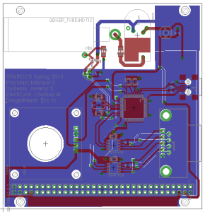
After being given the final schematic from the Electronics Engineer, I was able to begin layout. Because our board has predetermined (by PC/104) mounting hole locations and (by last semester’s chassis) size constraints, the first step was to set these dimensions. After defining the area of the board, the next step was to place components in a logical fashion. The first component placed was the PC/104 bus because it too has to be in a certain location. Resistor and capacitor networks were placed near the components they were supporting in an orientation that allowed for the straightest routing of traces. Once all components were placed, we were able to route traces. The VCC and GND traces were left alone until all other traces were routed. The VCC and GND traces were routed to planes and any traces were thickened. Per recommendation of the president, Chad, the area under the Geiger tube and DC-DC converter were kept clear of any planes as these are high-voltage areas.
Soldering / Assembly
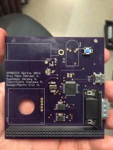
Once the PCB layout was complete, it was sent to a board house (OSHPark) to be manufactured. After the PCB and components were received, assembly of the board could begin. All components were soldered by hand using a fine tip soldering iron and very thin solder. The ATMEGA32U4 and the 16MHz crystal gave us issues. The ATMEGA32U4 was difficult because it had multiple traces next to each other. In order to solder it to the board, solder was applied to the pins in excess and bridged pins were cleaned up using solder wick. The challenge with the crystal is that the solder points were below the component. To attach the crystal, solder was applied to the pads and a heat gun was used to reflow the crystal to the board. All other components were easy to attach as they were either basic surface mount components or through hole components.
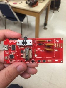
Two of our components were recycled from the SparkFun Geiger Counter Board. The two components are the geiger tube and a NPN transistor. In order to remove the components, a desoldering pump and solder wick were removed to remove solder. Once the majority of solder was removed, all that was required was to melt the solder and wiggle the pin loose.
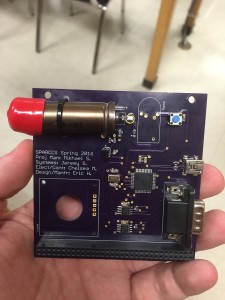
After removing the tube and transistor, they were easily attached to our final PCB. A zip tie was used to secure the tube to the board because it was the original method used in the SparkFun Board and it allows for a temporary attachment as our board is still a prototype.
Conclusion
In conclusion, the layout and assembly was fairly straightforward. The layout was constrained to the required dimensions to fit into the chassis. The assembly of the board was straightforward as well, the only challenge being removing the Geiger tube and transistor from the SparkFun board and soldering the ATMEGA32U4.
