DragonBot/Spring/2021
PCB Design Process
Author/s:Amha
Table of Contents
Introduction
Printed Circuit Board (PCB) helps to arrange electronic components in a compressed and efficient way. Instead of constructing electronic circuit through wire-to-wire connection, PCB has many advantages; it is compact, saves space, has resistance to movement, reliable and is efficient. This blog is about the PCB design process of the IMU shield for DragonBot
Process
Before designing the PCB shield, multiple tests were performed using a breakout board of MPU 9250 sensor. The breakout board has 10 pins; among those pins I used only five (VCC, GND, SCL, SDA and INT) during testing. The sensor utilizes the I2C communication protocol. After testing and approval of the sensor, I started designing the custom PCB using Eagle CAD.
First Iteration
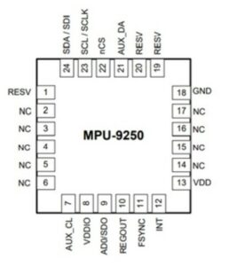
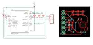
The actual processor (figure 2) has 24 pins, among the pins 9 of the pins were not connected to anything. Since I only used five pins during testing – VDD, GND, SCL, SDA, and INT, I designed the PCB circuit by taking the five pins into account and left the other pins unconnected. Once completed, the PCB design was sent to Chris for review.
Second Iteration
Based on the feedback from Chris, I learned that I have to check the recommendations from the data sheet on how to handle the unused pins. I also learned (from class lectures) that unused pins that need to be either grounded or connected to VCC, are recommended to be connected using a 10K ohm resistor. On the second iteration, I designed the PCB in response to the feedbacks and recommendations.
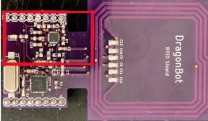
After the design was approved, it was sent for production merged with the RFID on a single board. The PCB is shown in the picture below:
Conclusion
The PCB design was produced successfully and worked as it was intended to work. The Eagle CAD training Chris gave was very helpful for me as I was able to design PCP after one training. The PCB design process gave me a hands on experience and I learned new skills that I will be able to apply in the future.


