DragonBot Maze Project Spring 2021
DragonBot RFID PCB Design and SMD Reflow
Author: Matthew Hillsman
Table of Contents
Introduction
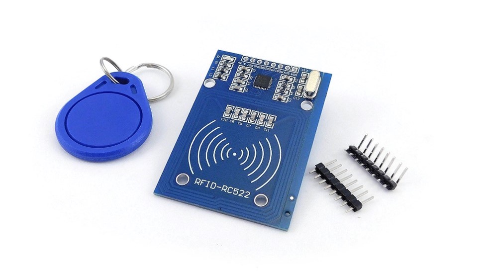
For the paperbot maze game, it was necessary to have a method for the robot to be able to detect cards so that the robot can identify monsters, weapons and other items placed throughout the maze. The method that team DragonBot chose to do this card reading was an RFID sensor. Therefore, a PCB shield needed to be designed for the RFID sensor so that it could be directly connected to the headers of the 3Dot board.
Design Considerations
During the design of the RFID PCB, there were many factors that needed to be considered. One aspect that needed to be considered was the placement of the antenna. Some tests were performed to see what options we had for the placement of the antenna, and those tests can be found here.
Another important aspect that needed consideration was the impedance of the antenna coil. The impedance of an antenna is very tricky, and designing one requires a lot of detailed considerations on all the capacitors and inductors used, the thickness of the traces in the coil, and the distances between components that are directly connected to the antenna among other things. All of these would need to be considered and fine-tuned. Because of this, it was decided that the antenna design would follow a pre-established working design for the MFRC522. The board that this replica attempted to follow can be found here.
Schematic Diagram
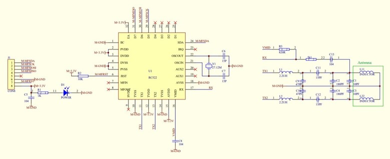
The initial schematic design was copied from the design of the board that was being followed.
The above schematic in figure 2 can be found here.
The PCB that was designed used these same value components that are shown in the schematic diagram in figure 2. The intent was to keep the values as close to the original as possible because of the possible impedance issues previously mentioned.
PCB Design and Layout
First Design Iteration
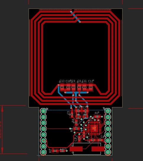
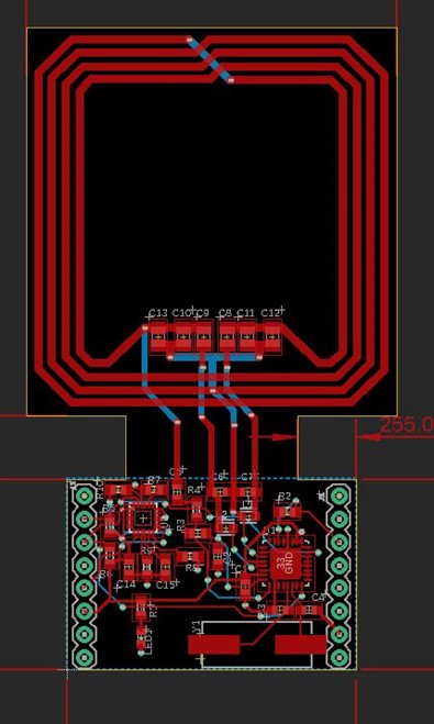
During the design of the first iteration of the PCB, the schematic was created per the example given and the initial layout was created. The antenna layout and traces were copied from the example that can be found here.
The first iteration design of this PCB had the antenna very close to the header pins. This would make the PCB impossible to install into the Paperbot chassis as the top part is too wide, even if the entire wooden back of the chassis was removed, the PCB would still not be able to fix. This iteration also used 6mil traces for all of the signal lines, while 8mil is the minimum desired trace size. There were also several angle errors with this design, which needed correction.
Second Design Iteration
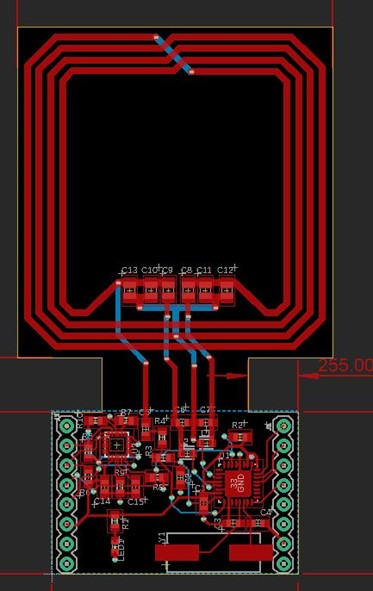
In the second iteration the problems associated with the first iteration were corrected. The problem with the antenna not being able to fit into the chassis was corrected by extending the antenna so that it is on the outside of the chassis and would be able to fit with minor modification to the wooden back panel. The traces were made larger and the errors with some of the angels were also fixed.
In addition to fixing the above problems with the first iteration, in this iteration of the design also included the IMU circuit which included a gyroscope and a compass, and was intended to give the robot the ability to self-balance itself, as well as be able to give the robot its orientation relative to north. This circuit was designed by team DragonBot’s control engineering, and the design process of the circuit can be found here.
The only problem associated with this design is that since the RFID IC used the SPI communication protocol, there were no additional pins available to use in the event that we needed to use the wheel encoders.
Third Design Iteration
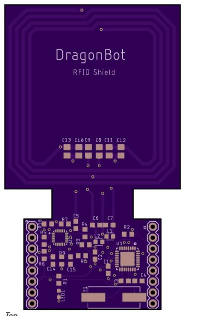
In this final iteration of the RFID PCB design, the MFRC522 IC was changed from using the SPI protocol to using the I2C protocol, so that the additional pins used by the SPI bus could be freed up to use as digital input/output pins if desired. The I2C address needed to be set, and for that the procedure found in the MFRC522 IC’s data was used to set the address. The datasheet for the MFRC522 IC can be found here.
Sending Design to manufacturer
After receiving approval on the final iteration of the PCB design, one final modification was made and a silkscreen bearing the name of team DragonBot was added for a more personal touch to the board. The board files were then uploaded to Oshpark and 6 PCBs were produced in total.
PCB Assembly Procedure
After receiving the PCB from the manufacturer as well as all the components needed for the build, 5 of the PCB boards were assembled.
First PCB assembly
Only one PCB was assembled initially so that it could be tested and confirmed to work. The remaining 5 PCBs that were assembled were only done after the first PCB was tested and confirmed working, and so that a time efficient assembly procedure could be developed so that the remaining PCB assemblies did not take as long.
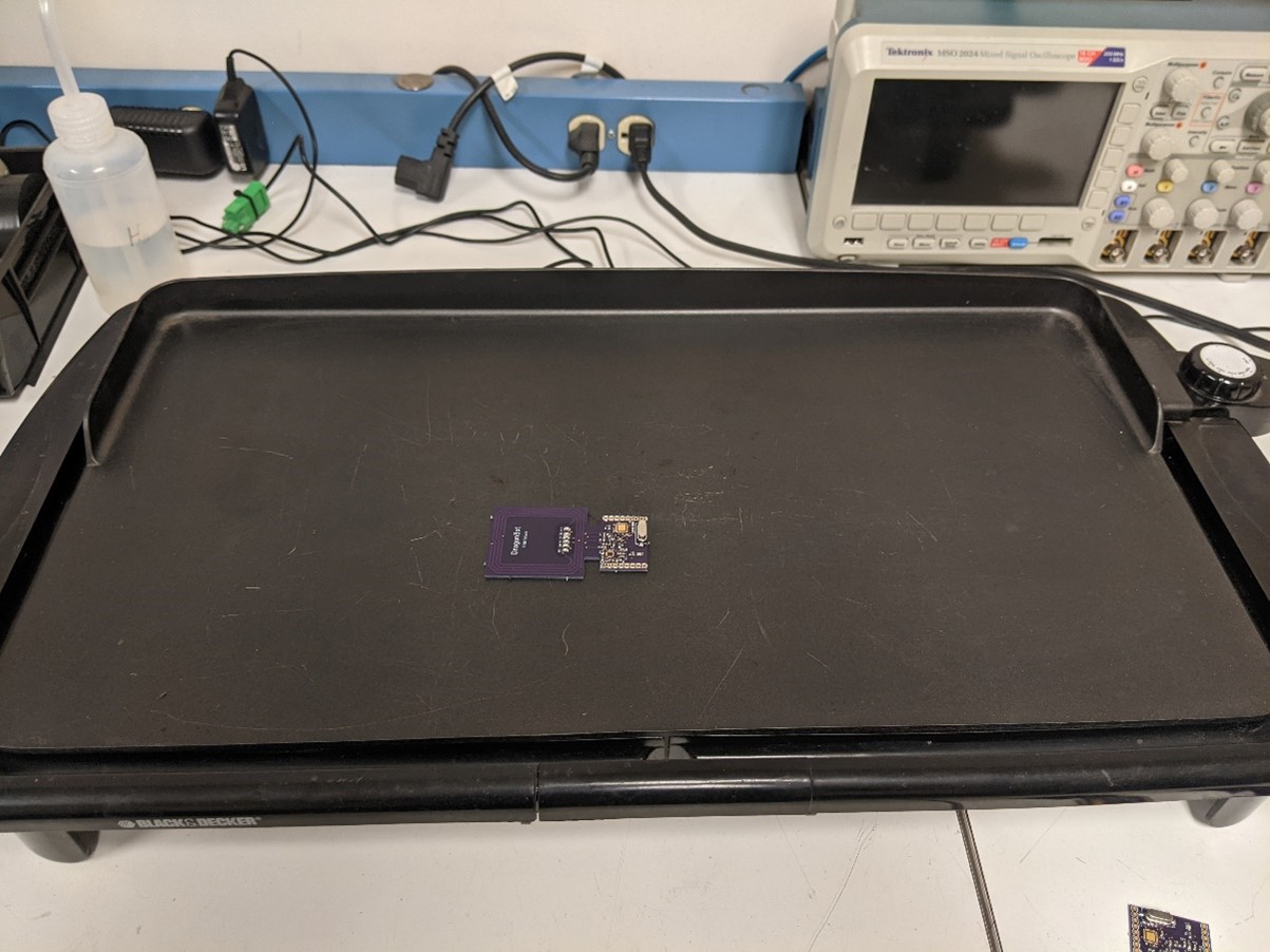
For the first board that was assembled, low temperature solder paste was applied to all the surface mount pads. Each component was then placed on top of the solder paste and aligned with it’s pads on the board. The PCB was then placed on a hotplate and the temperature was monitored with a ranged thermometer so that the PCB would not burn. After the solder paste had melted fully and the components seated into position, the PCB was then visually inspected for solder bridges and other issues under a microscope.
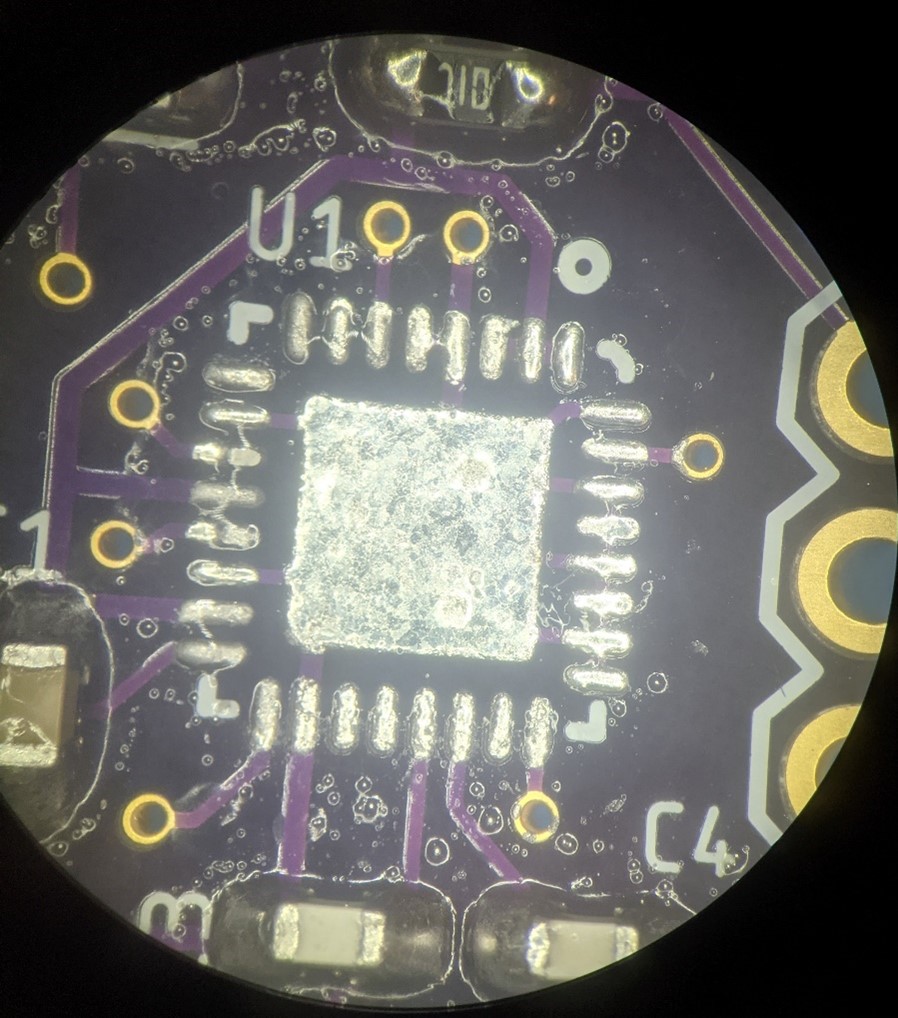
Upon visual inspection, it was found that there were many solder bridges on the pins of the MFRC522 IC. This was corrected by drag soldering across the pins and reinspecting under the microscope. This correction however was a time-consuming process, which I did not wat to repeat in the assembly of the remaining 4 PCB assemblies.
Remaining PCB assemblies
For the remaining boards that were assembled, soldered paste was applied to all surface mount pads except the pads of the MFRC522 IC as well as the MPU-9250 IC. All the passive components were then placed on top of the solder paste, in their correct position.
After placing all the components except the ICs on the solder paste, the PCBs were then placed on the hotplate and the temperature was monitored using arranged thermometer.
After removing the PCBs from the hotplate and allowing them to cool, the components were then visually inspected under a microscope for misalignment and solder bridges.
After the passive components were visually inspected, I then placed solder on each of the pads of the ICs using a soldering iron. Using tweezers and viewing from the microscope, I then carefully aligned the ICs with their respective pads on the board. Then using a heat gun with the air turned to the lowest blow rate, I began to heat up the solder underneath the ICs and allowed it to melt until the ICs were seated in place.
After installing the ICs using the method described above, I then visually inspected each of the pins of the ICs under a microscope, looking for unconnected pins and solder bridges. Some minor rework was needed on a couple of the boards, however, using the method of installing the ICs by hand after all the other components was found to be a more time efficient method of assembly then the first PCB assembly.
Verification of Functionality
After testing all the components I then connected the PCBs to the 3dot board and first loaded the I2C_scanner.ino example for the wire library on the Arduino IDE. More information about the wire library and the example code used can be found here. Using the I2C_scanner, I was able to see the I2C addresses of both ICs that were connected to the boards and verify that the ICs were at least communicating with the 3Dot board properly. After checking the boards using the I2C_scanner, I then loaded test code for both the RFID as well as the IMU and was able to confirm functionality on the PCB.
Of the five boards that were assembled, only one board failed the functionality tests. The on-board LED was not even lighting up, so I tested the voltage input and was able to quickly determine that there must have been a short between the 3.3V bus and ground somewhere underneath one of the ICs. I did not attempt to rework this board however, because I already had four boards working, which was all that was necessary for the project.
Conclusion
In conclusion, due to the need for a way for our robot to detect a card that was placed on the maze, team DragonBot decided to use an RFID sensor to perform this action, and therefore the this PCB was designed and assembled. During the process of the design, I was able to get valuable practice with the layout of a PCB, the assembly of surface mount components, and troubleshooting and rework of problems with the board. This PCB design worked well, and as a result of this design, Team DragonBot’s robot was successfully able to detect cards that were placed on the maze.

