Pre-Lab 4B: Interrupts
Table of Contents
The Real World
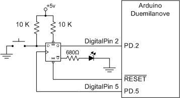
In the lab you are going to write an interrupt service routine to respond to the push-button debounce circuit included with your proto-shield and shown here.
Increase Resolution
Question 1 After reset is applied and before clock is asserted, will the LED be ON or OFF. Explain your answer.
Question 2 Assuming the current into the D input of the Flip-flop is negligible, what current, if any, would flow through the pull-up resistor wired to the button when the button is pressed?
The introduction of the push-button on the proto-shield brings us, for the first time, in contact with the real world. Here are two real world problems that came up during the original design of the circuit shown in the schematic. My first design simply wired the button and resistor to the input of the micro-controller.
Rise and Fall Times
Between logic 0 and logic 1 there is an undefined region. Electrical signals have a finite period to transition through this region, technically known at rise and fall times. For some micro-controller inputs this can be no more than 20 nsec. If this specification is violated the input may start to oscillate causing havoc within the device. Next, the input circuits of MOS devices, like our AVR micro-controller, can be characterized as capacitive in nature (can be modeled to the first order by a capacitor). For some inputs this capacitance can be as great as 10 pF (pico = 10-12). Now, let us assume an external pull-up resistor of 10 KΩ. Given this information we come up with a “back of the envelope” calculated time constant (RC) of 100 nsec. Clearly, we have a problem. I solved this problem by adding a TTL device between the switch and the micro-controller. The input of the 74ALS74 Dual D-Flip-flop can be characterized as resistive in nature (can be modeled by a resistor). Combined with a pull-up resistance (10 KΩ) the input problem is ameliorated. The output of the 74ALS74 TTL device goes directly to the input of the AVR micro-controller solving the transition problem. This new faster circuit however introduces its own problems as discussed in the next section.
Debounce
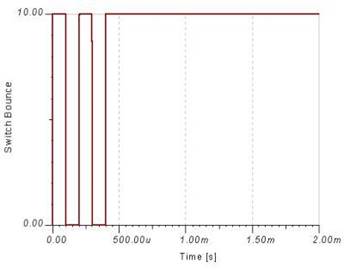
When you press a button, its contacts will open and close many times before they finally stay in position. This is known as contact bounce. Depending on the switch construction, this mechanical contact bounce can last up to 10 or 20 milliseconds. This isn’t a problem for lamps, doorbells and audio circuits, but it will play havoc to with our edge-triggered interrupt circuitry.
With respect to the waveform above, all our switch debounce solution has to do is filter out these transitions. This can be done in several ways. For some simple electrical solutions visit http://www.patchn.com/Debounce.htm. For our solution, I added a D flip-flop which is clocked at a frequency less than 50 Hz (1/20 milliseconds). This digital circuit acts as a low pass filter blocking the AVR interrupt circuitry from responding to any of these additional edges. Another solution, is to disable the external interrupt during the switch bounce time. This solution acts again like a low pass filter, and thus removes the need to the external D Flip-Flop; however, it does not address the rise and fall transition time concern.
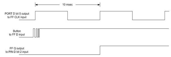
Question 3 In this question you are going to modify the waveform diagram with inputs D and CLK of the Flip-flop and output Q as shown below. The clock input (CLK), shows two (2) clock cycles with a period of 10 milliseconds each. The D input labeled “Button to FF D input” shows the switch initially pressed and the input at logic zero. The button is released just before the first clock edge. The output of the debounce circuit for these input conditions is shown as “FF Q output.”
To investigate how the debounce circuit works, I want you to move the point at which the button is released (the bouncing part of the waveform) in the Figure below. Move the switch bounce so its occurs somewhere relative to the leading edge of the clock signal labeled “Port D bit 5 output to FF CLK input”. The exact phase relationship of the switch bounce to the clock edge is left to you. Based on these two inputs (Button and CLK) to the D Flip-flop redraw output signal Q.
Vertical lines
Question 4 Using what you have learned in class and from chapter 10 in your textbook, answer the following:
- Your program has two interrupts enabled in addition to reset: external interrupt request 0 (INT0), and timer/counter 1 overflow interrupt (TIMER 1 OVF). While the program is in the ISR for INT0, the INT0 flag is set. What will happen? Explain.
- If both interrupt flags set at the same time, what program address (the actual number) will be loaded? Hint: see ATmega328P IVT.
- What should be the last instruction in the ISR?
Question 5 INT0 in an ATmega328P is connected to a normally high switch. It is required that the value of PORTB0 should toggle when any logical change occurs.
1. Initialize INT0 to generate an interrupt when the pin has any logical change:
______ r17, 0x_____
______ EICRA, _____
2. Enable external interrupt 0:
______ EIMSK, _____
3. What other instruction is needed to enable INT0?
What Should I Turn In?
Turn in the following material three pages. Make sure all your original work is in your Lab Notebook. All written material must be typed or very neatly done in ink. Once again please do not copy.
Page
- Title page with the pre-lab number, your name and picture, today’s date, and the day your lab meets.
- The problem statements (remove explanatory text) and solutions to all pre-lab questions. Circle and/or highlight your answers. Make sure all your original work is located in your lab notebook.


