Pathfinder Solar Array Generation 2 Summary Blog Post
Author/s: David Born, Eduardo Charcas
Table of Contents
Executive Summary
by David Born
Fall 2018 Pathfinder Solar Array Generation 2 implements a new design for the power distribution of the solar array. The new design allow for a more information about the cells providing power for quicker debugging of the system. The design also allows helps lower the risk short circuits.
Program and Project Objectives
by David Born
Program Objectives
The design of the Fall 2018 Pathfinder project was taken from NASA’s Mars Exploration Rovers, Opportunity and Spirit. The Pathfinder will be designed to be self-sufficient using solar panels. The solar panels should able to recharge the Pathfinder’s battery allowing it to traverse rough terrain. The solar panels must also articulate to track the sun, maximizing the amount of solar power received.
Project Objectives
The Pathfinder Solar Array project will offer an opportunity to build and study articulating custom solar panels which are able to track the sun and enter/exit a cocoon state. The panels will be modular allowing remote identification (telemetry) and astronaut replacement of a broken module. Additional telemetry requirements include providing information on articulation angles, panel voltages, charging current, and battery fuel level. A cocoon state shall be used during simulated launch, dust storms, and operation over steep terrain. A new design for mounting solar cells was will be implemented in order to minimize the chance of short circuits. Updated design will also change the panel connection path (wires) to run underneath the wing, tail, and base plates as opposed to the previous generation upper connection path. Based on the fixed size of the articulating solar panels, efficiency, sun’s path during time of mission, and the mission objective, the project will fulfill an 8 charge time and batteries for the rover. The Mission Objective is to traverse the same course as defined for the Fall ’16 Pathfinder.
The form factor of the solar panels will be similar to the panels on the Spirit and Opportunity Mars rovers. Sizing of the panels will be consistent with the existing chassis and meeting the form factor of the Mars rovers. Specifically, the size of the panels relative to the size of the chassis will be identical to the Mars rovers (scaled model).
Mission Profile
by David Born
The S’18 Pathfinder will commence it’s Mission by first exiting a “cocoon state” in front of CSULB’s library, then traversing .09 miles to it’s destination charging station. To reach it, the Pathfinder will need to traverse up and down a set of 3 steps. GPS Navigation mode will use 11 predefined checkpoints including start and finish L-L coordinates. Along the way, the Pathfinder will operate in articulation mode, in which the solar panels will track the sun and provide current telemetry of each of it’s 36 cells to a sync’d Arxterra App user within Bluetooth range.
Project Features
The system will have a custom solar cells array. This will be done using 17 strings in parallel of 3 solar cells in series together in series to fit the customized solar shape of the aforementioned rovers (see Spirit’s layout in Figure 1). The solar panels will be configured to be in the form factor of the solar panels on the Opportunity and Spirit rovers.
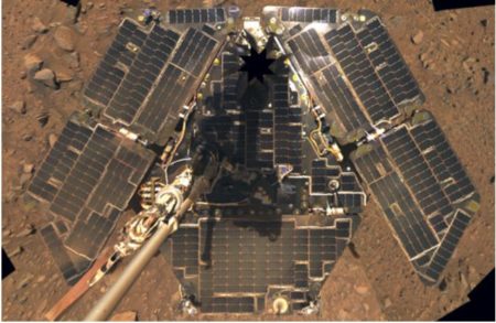
Figure 1: Spirit Rover Panels
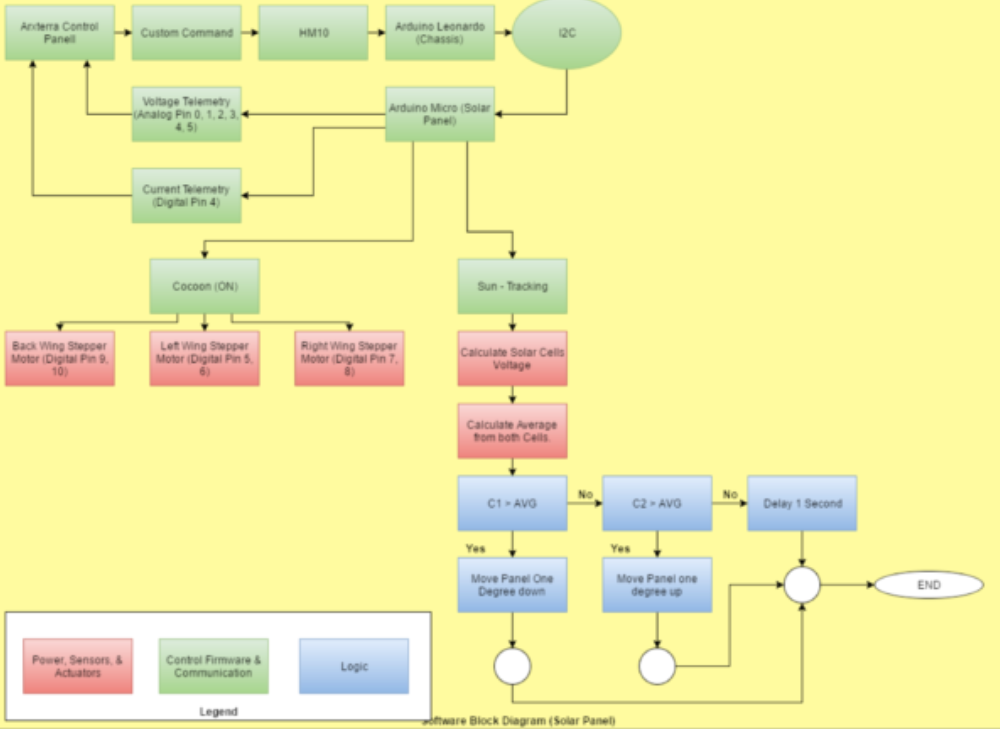
The system will maximize solar power input by tracking the sun with the system outlined in Figure 2.
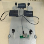
The product is currently in the prototyping phase (see Figure 3)
Requirements
By: David Born
The design of the Fall 2018 Pathfinder project was taken from NASA’s Mars Exploration Rovers, Opportunity and Spirit. Its mission is to travel from the front of CSULB’s library down .09 miles to it’s destination charging station. The goal of the Solar array system is to enable the Pathfinder to charge after reaching the charging station.
Engineering Standards and Constraints
by David Born
Review and show compliance with constraints on the project imposed by The Robot Company (i.e., CSULB) and Project Stakeholders. Specifically include University and applicable environmental, health, and safety standards and those safety standards specifically associated with the product (e.g., Children’s Toys).
Applicable Engineering Standards
- IEEE 29148-2018 – ISO/IEC/IEEE Approved Draft International Standard – Systems and Software Engineering — Life Cycle Processes –Requirements Engineering.
- NASA/SP-2007-6105 Rev1 – Systems Engineering Handbook
- Bluetooth Special Interest Group (SIG) Standard (supersedes IEEE 802.15.1)
- C++ standard (ISO/IEC 14882:1998)
- Federal Communications Commission (FCC) Relevant standards for a product implementing a 2.4GHz radio, FCC Intentional Radiators (Radio) Part 15C, and Unintentional Radiators FCC Part 15B for CPU, memories etc.
- NXP Semiconductor, UM10204, I2C-bus specification and user manual.
- ATmega16U4/ATmega32U4, 8-bit Microcontroller with 16/32K bytes of ISP Flash and USB Controller datasheet section datasheet, Section 18, USART.
- USB 2.0 Specification released on April 27, 2000, usb_20_20180904.zip
- Motorola’s SPI Block Guide V03.06
Environmental, Health, and Safety (EH&S) Standards
CSULB College of Engineering (COE) Safety Resources. Start your search for applicable CSULB COE Safety Standards and Procedures here. Please review and acknowledge if any safety issues as defined by the COE applicable to your project. For example, the closest safety constraint for a linear actuator is for use of the Hydraulic Press located in the Engineering Technology (ET) Building Lab. Here is a link to the Hydraulic Press Safety document.
CSULB Environmental Health & Safety (EH&S)
IEEE National Electrical Safety Code (NESC)
NCEES Fundamental Handbook (FE) Reference Handbook
ASTM F963-17, The Standard Consumer Safety Specification for Toy Safety, is a comprehensive standard addressing numerous hazards that have been identified with toys. In 2008, the Consumer Product Safety Improvement Act of 2008 (CPSIA) mandated that the voluntary toy safety standard in effect at that time become a nationwide mandatory children’s product safety rule.
Disposal of Hazardous Waste including Electronic and Solar Cells
CSULB Physical Planning & Facilities Management (PPFM) Environmental Compliance Electronic Waste Handling and Disposal Procedures. These procedures shall be followed for the disposal of all batteries.
Program Level 1 Requirements
By: Eduardo Charcas
Project/Economic
Subcategories: Cost, Extensibility, Interoperability, Maintainability, Quality, Marketability, and Schedule
The Pathfinder Solar Array shall be constrained to not exceed Cost of $250.
All project Schedules shall be constrained to a completion date of Tuesday December 18, 2018. Project completion includes documentation and materials purchased by or loaned to the project.
One of the Economic Factors affecting our solar array is the cost of rapid prototyping. Purchasing electronic components, hardware and manufacturing costs will be a limiting but not determining factor. To demonstrate that the wing panels shall be in the form factor of opportunity & spirit
Social and Ethical Maintainability: Disassembly and Reassembly of the one of the solar modules shall be constrained to less than 3 minutes per module. Disassembly: The Pathfinder Solar Array is clear of all other electronic and mechanical sub-assemblies. All electronic and mechanical sub-assemblies and associated connectors, sensors, and actuators including motors are disconnected. A functional test of the robot is conducted after reassembly to confirm its functionality. All project may reference a cable tree as well as an assembly diagram as necessary. This requirement is demonstrated/verified on the last day of the schedule. Projects may request a waiver with justification.
Subcategories: Accessibility, Aesthetics, and Usability
Wiring Aesthetics shall be nice and clean with the usage of terminal blocks, 100 mil contact pins and headers, 2.0mm PH series JST connectors, and barrel connectors. Handling Precaution for Terminal and Connector will be in compliance with JST documentation.
To enhance Aesthetics, the robot shall be designed in such a way that there are no dangling or exposed wires. Connectors will used between all electronic and electromechanical components. Jumper wires will not be used, ribbon cables are preferred.
To enhance Aesthetics, the form factor of a robot modeled on a real or fictitious robot shall be constrained by the original. For example, Goliath should be a scale model of the real Goliath 302 tank. Projects may request a waiver with justification.
Usability of the robots shall be enhanced by adding autonomous functions and/or by use of the Arxterra phone application as dictated by the assigned mission.
Manufacturability of the solar array will require different resources, such as 3D-Printing, laser cutting, soldering, drilling, cutting, and designing.
Subcategories: Constructability, Size, Weight, and Power (SWAP)
Constructability of Pathfinder Solar Array shall be documented at the CDR and approved by the president of the TRC robot company. Constraints imposed by this requirement include the use of bushing or bearings in all moving and rotating parts. Interlocking Hinges with latching mechanism. No gaps greater than 1 millimeter, and immediate access to all external connectors (USB, switches).
The Size of the electronics enclosure, shall be constrained to be no greater than the Arduino Uno board, Power Hub PCB, and associated mounting hardware.
Power from and to all panel motors shall be provided by the 12V battery. The battery is a Lithium Polymer LiPo battery. All Safety regulations as defined in Section 4.3 Hazards and Failure Analysis of this document shall apply to the shipping, handling, storage, and disposal of LiPo batteries.
Back of the envelope calculations and experiments shall be conducted to set the diameter of Power carrying wires. Follow the American Wire Gauge (AWG) standard when defining the diameter of power carrying wires. This work to be completed and documented by the CDR.
Environmental Health and Safety (EH&S) Standards
Subcategories: Environmental Standards, Sustainability, Toxic waste (Solar panels), Health and Safety, Ergonomics
All standards, codes, and regulations as defined in the “Engineering Standards and Constraints” Section of this document shall apply.
Functional
Software shall be written in the Arduino De facto Standard scripting language and/or using the GCC C++ programming language, which is implements the ISO C++ standard (ISO/IEC 14882:1998) published in 1998, and the 2011 and 2014 revisions. Required exceptions to this standard can be found here.
All Pathfinder Solar Array robots shall be controlled via Bluetooth 4.0 in compliance with the Bluetooth Special Interest Group (SIG) Standard (supersedes IEEE 802.15.1).
Project Level 1 Functional Requirements
By: Eduardo Charcas
In Summary, the project specific Level 1 Functional Requirements:
- Should have solar system array attached to chassis.
- Should recover from tipping over.
- The Pathfinder should be able to articulate a total of 75 degrees to track the sun.
- The Pathfinder should enter and exit the cocoon state by Arxterra app user input.
- Solar PCB’s Should be able to read current and voltage.
- The pathfinder battery should be charged by the solar array
System/Subsystem/Specifications Level 2 Requirements
By: Eduardo Charcas
2.1 Form Factor
Wing modules shall be in the form factor of Opportunity & Spirit
Looks like Opportunity & Spirit.
2.4.1 Arxterra Robot App
The Arxterra robot app shall receive telemetry data from the solar array (voltage and current data).
2.5.1 Assembly/Disassembly
Shall assemble and disassemble the solar array at the module level (2 dummy cells and 1 smart cell) within 3 minutes
2.5.2 Manufacturing
Shall have at least one Custom PCB on the cell level
2.5.3 Module Construction
You shall demonstrate a functional module (module being 3 cells)
Module is assembled and transmits powers.
2.5.4 Module Voltage
Will have a fully assembled module that provides 12 or more Volts
Module provides required voltage.
2.5.5 Slave PCB
Verify functional slave cell (slave has power, voltage, current) that shall have 2 slave cells that provides 4 or more volts per cell
Slave cell provides voltage.
2.5.6 PCB Series
Connect master to the two slave cells and ensure addition of voltage.
Cell PCBs add voltages in series.
2.5.7 PCB Communication
Should have master communicate thru an Uno with functional code.
ATtiny communicates with Arduino Uno.
2.5.8 Wire Protection
Cable shall be organized so as not to short circuit, 0V provided on a given cell, the system
PCB soldered cells have no short circuits.
2.5.9 Power Combination
Power Hub PCB shall sum panel level currents
Power PCB adds inputs in parallel
2.6.1 Battery Charging
Shall have a Functional Battery charging
2.6.2 Power Charging
Charger shall regulate voltage to 12V and charge battery in optimal sunlight for up to 5 hours
Charger Output doesn’t go above 12V.
Measure the voltage output of the charger between the terminals of the charger battery output.
2.6.3 Electrical Protection
Electronics should have an enclosure that fits between chassis top plate and solar array base panel for the Arduino Board and other hardware
By: Eduardo Charcas
| Mass Report | ||
| Part | Actual Weight (g ) | Total Weight ( g) |
| Solar Cells | 220 | 220 |
| PCB | 120 | 120 |
| Acrylic Panels | 500 | 500 |
| Wiring | 40 | 40 |
| Battery | 2600 | 2600 |
| Voltage Regulator | 100 | 100 |
| Total Allocated Weight | 3580 | 3580 |
By: Eduardo Charcas
| Power Report | |||||
| Part | Expected Current Collection | Measured Current Collection | Expected Voltage | Measured Voltage | Uncertainty (%) |
| Single Solar Cell | 0.067 A | 0.07 mA | 3V | 2.8V | 15 |
| Single Solar Module | 0.24 A | 0.3 A | 9V | 15.65 V | 10 |
| Battery | TBR | TBR | 12V | 10.55 V | 25 |
| Total Power | 0.307 A | ||||
| Allocated Power | 0.4 A |
Project Report
By: David Born
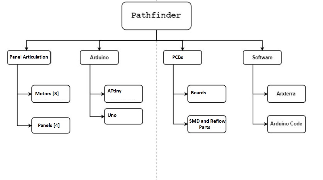
Project WBS and PBS
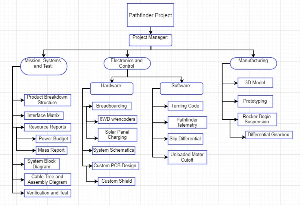
The work breakdown structure describes the major responsibilities of each engineer working on the project. The Electronics and Control division has been divided into two main categories, software and hardware. The Manufacturing division was primarily responsible for the overall fabrication of the Pathfinder and detailed SolidWorks model. And finally the Mission, Systems and Test engineer is responsible for the integration of all these different divisions.
Cost
By: David Born
| Item | Unit Price ($) | Units | Tax | Total | |
| 1 | Arduino Uno | 19.50 | 1 | – | 19.50 |
| 2 | Uxcell 39 Plastic Shell 8p8CPCB Jack Ports | 10.77 | 1 | 0.83 | 11.60 |
| 3 | Willwin 10PCS Shielded RJ45 | 8.20 | 2 | 1.27 | 17.67 |
| 4 | Cat 6 Ethernet Cable 1.5ft (6pack) | 8.95 | 3 | 2.08 | 28.93 |
| 5 | 20x25x1, Percionaire EZ flow li Front panel Merv4 | 31.47 | 1 | 1.89 | 33.86 |
| 6 | Conn IC dip Socket 8POS | 6.40 | 1 | – | 6.40 |
| 7 | IC MCU 8BIT 8KB FLASH 8DIP | 4.96 | 1 | 0.86 | 22.23 |
| 8 | 50 mm Stroke Linear Actuators | 25.00 | 3 | – | 113.00 |
| 9 | 8 channel Relays | 10.88 | 1 | – | 10.88 |
Total $257.41
Schedule
By: David Born
The following schedule was the recommended timeline for finishing the project.
Burndown and/or Percent Complete
By: David Born
The project has finish its first iteration of PCBs and is ready for the second generation. The project still needs the PCBs to be modified after some mistakes and con ops failures. The articulation is incomplete. Thus the project is about 30% complete.
Concept and Preliminary Design
Literature Review
By: Eduardo Charcas
Theoretical background, concepts involved in the design process and a summary of the key literature and online resources are provided in the Arxterra links below.
In this Solar Array Generation 2 , there was further and successful development of the solar cells mounting onto the panels, and using PCB’s that were soldered onto the solar cells, there was successful current and voltage measurements that proved proof of concept at the module and cell level. More manufacturing and budget resources are needed to further improve and manufacture solar panels out of aluminum. Articulation is still a remaining issue that will need to be solved by future generations..
Design Innovation
By: David Born
Creative solutions introduced with this generation:
The solar cells were organized into modules of 2 slaves and 1 master. The connection between cells will on the underside of the panels so that the final design looks cleaner and has less short circuiting. The connections between cells will be ethernet cabling instead of jumper wires. Each module will have an ATtiny to allow the voltage and current of individual modules to be reported to the user.
Conceptual Design / Proposed Solution
By: Eduardo Charcas
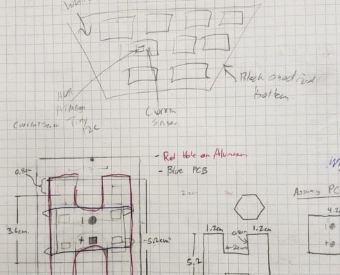
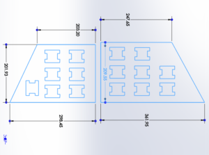
Figure 8 Preliminary design measurements were taken of the generation #1 Solar Array panels, with notes on requirements.
Figure 9 shows conceptual drawings of ideas first proposed by the students of how to solve the issue of transmit power and read voltage and current at the cell and module level.
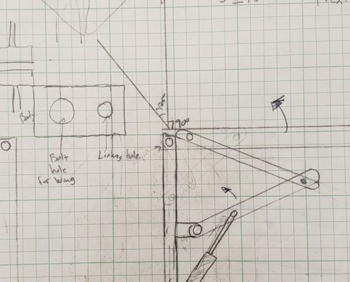
Figure 10 shows conceptual drawings of what mechanism would be used in conjunction with the linear actuators to articulate the panels.
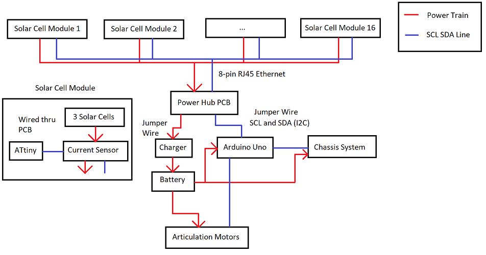
Figure 11 is was a preliminary block diagram of the conceptual framework of how the solar array system would be.
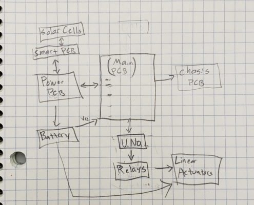
Fig. 11: Block Diagram
System Design / Final Design and Results
By: David Born
The final design tried to use the bottom of the panels so that the topside was clear of wiring. The design required that the connectors be able to fit below the panel and not hit the middle as the PCB sitting inside the hole.
The major subsystems of the design were the ATtiny85 measurement of the current and voltage. The Arduino coding provided in the Firmware section allows the ATtiny to do so. The Power hub PCB allows the current generated from all the panels to be added together before going to the battery. The use of ethernets cords reduces the chance of short-circuits and exposed wiring which makes the system much safer to use.
The final design so far has not differed from the conceptual design
System Block Diagram
By: David Born
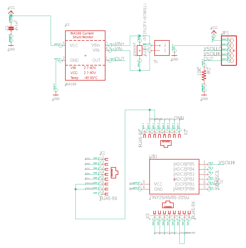
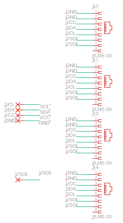
Using an INA 169 and an ATtiny85, the Solar Array can report to the Arduino Uno what the current and voltage of each module are outputting. See link below for ensuring that the amperage is sufficient for charging. Figure shows the connections of each unit in the Solar Array system.
Interface Definition
By: David Born
As defined in the mission profile, the Pathfinder will be allowed to travel a course on the upper campus of CSULB. This system is designed to replicate the Spirit & Opportunity Mars Rovers. The program objective is to be self-sufficient. In order for this system to be successful with it’s mission, the two systems; Chassis & Solar Panel, must work together with one another. The Solar Panel will be in charge of supplying power to the battery, and the Chassis will then be able to use this battery and travel the course.
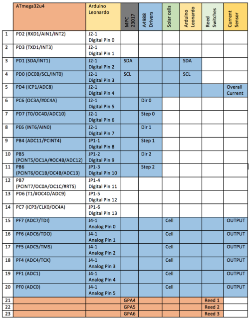
Figure 13: Interface Matrix
Modeling/Experimental Results
By: Eduardo Charcas
Following are the modeling tasks planned and completed along with associated post.
- Amperage Testing of Solar Cells
- Articulation Using Linear Actuators
- Solar Array Panel Design Using Solidworks
- Solar Panel PCB’s
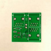
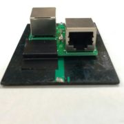
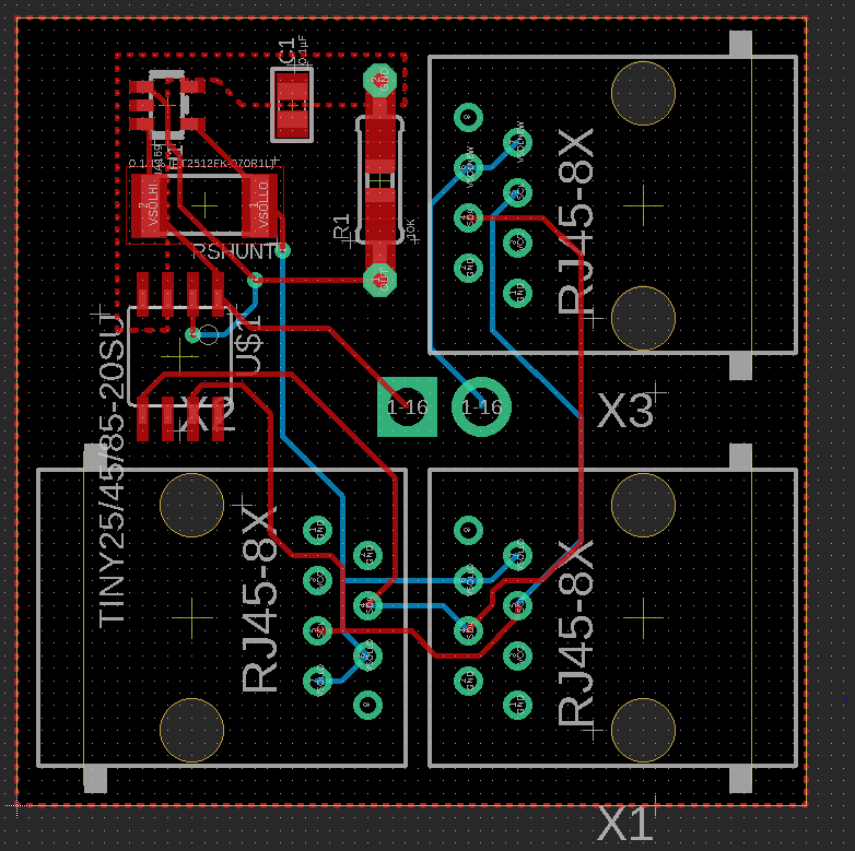
Most of our work was in the rapid prototyping of a single module containing a master and two slave cells. Figure 14 shows the custom PCB that was designed and manufactured , is attached to each solar cell (Slave & Master)
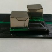
Figure 15 and 16 show a Slave Cell (PCB with 2 Ethernet connectors +Solar Cell) , which only functions as a collector and transmitter of the power collected by the solar cell.
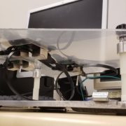
Figure 17 and 18 show a single module assembly with laser cut acrylic panel printed through CSULB I-SPACE.
Mission Command and Control
By: David Born
The Solar Array system should be able to enter and exit a cocoon state, deploy wings to approximately 100o to -30o against the horizontal respectively, when commanded. The system should continuously give the user feedback on the total current and voltage being generated from the array. The system should provide the current and voltage being generated from each module when asked the Arxterra Robot App. The system should also continuously give information on any module not providing minimum voltage and current (AKA broken module).
The following example commands are in the form: Command -> [Activity] -> Feedback
Enter Cocoon -> [Brings wing angle to 100o] -> Notification displays “Entered Cocoon”
Exit Cocoon -> [Brings wing angle to -30o] -> Notification displays “Exit Cocoon”
Cycle Module -> [Cycle which module voltage and current is being displayed] -> Displays new module information
Electronic Design
By: David Born
The system uses PCBs soldered to the cells from the bottom of the cell. Each slave cell has 2 RJ45 Ethernet headers attached. The PCB attached to the master has 3 RJ45 Ethernet headers, an INA169 Current Sensor, and an ATtiny85. The Master cells were designed to put the 2 slaves and itself into series, to ensure at 12V across the module, while also putting itself and another module in parallel, to sum the amperage. The ethernet headers and cords were the cheapest option for wiring found. The INA 169 Current Sensor eagle design was found on Adafruit so allowed for easy customization. The ATtiny was chosen because of its accessibility and it uses arduino coding language which was consistent with previous generations coding in this project.
PCB Design
Firmware
Section Author: Eduardo Charcas , Code by: Alex Nguyen, Derick Phan
The firmware that was developed was to have a complete I2C communication system for the 51 solar panels on the Pathfinder. The I2C communication is needed to have the Attiny85, slaves, communicate with the Arduino Uno, master, if one of the solar panels start failing. We would be able to do this by having the slaves send current data to the master. The master would interpret the data and determine which series of solar panels are starting to fail.(Alex Nguyen)
Mission Software/Electronics:
First, the Arduino would need to be set as ISP by uploading ArduinoISP onto the Uno. Second, you would change the board to Attiny85 with internal 8MHz and Arduino as ISP and connect a 10uF capacitor to reset and negative lead of the capacitor to ground. This changes the Arduino to be able program the Attiny85 without constantly resetting. Gathered from github Table 1 Section 6, the slave code includes a file file instead of file because it was giving me a constant error. After all the slaves have been programmed you would need to switch the board back to the Uno and program the master code onto the Uno. I also tested that the Attiny85 worked by using the blink test from source Table 1 Section 8. Lastly, I had a digital multimeter attached to the INA 169 current sensor to double check that there was a current being sent to it and I got current values from 30mA up to 300mA.
Arduino Code: (By Alex Nguyen, Derick Phan)
Master Code:
// Master - UNO
#include // File that includes all the necessary code for I2C
int button = 1; // Initalizing variables and constants, button not used in code, was
used for testing
int c;
void setup() {
pinMode(button,INPUT); // Setting button as an input, this was used for testing with I2C
Wire.begin(); // Begin transmission of I2C
Serial.begin(9600); // Begin Serial with baud of 9600
}
void loop() {
Serial.println("Slave 1"); // Prints Slave 1 onto the Serial Monitor before requesting data
from Slave 1
Wire.requestFrom(1,1); // Requests Data from Slave 1 with 2 bytes
while(Wire.available())
{
c = Wire.read(); // Saves the recieved data from Slave 1
Serial.println(c); // Prints the data onto the Serial Monitor
delay(500); // Added a delay to make the data more readable
}
Serial.println("Slave 2"); // Prints Slave 2 onto the Serial Monitor before requesting data
from Slave 2
Wire.requestFrom(2,1); // Requests Data from Slave 2 with 2 bytes
while(Wire.available())
{
c = Wire.read(); // Saves the recieved data from Slave 2
Serial.println(c); // Prints the data onto the Serial Monitor
delay(500); // Added a delay to make the data more readable
}
}
Slaves Code (With just change of numbering):
// Slave1 - Attiny85
#include // File used for slave component, I tried using but it
gave errors.
int current_sensor = 3; // Initalizes variables and constants
int VOLTAGE_REF = 5;
int RS = 10;
int sensorValue;
int current_example;
void setup() {
pinMode(current_sensor,INPUT); // Sets pin mode of INA169 as input
// sensorValue = analogRead(current_sensor); // Used for Testing
TinyWireS.begin(1); // Sets up this Attiny85 as Slave 1
TinyWireS.onRequest(RequestData); // Testing for I2C communication
// TinyWireS.onRequest(RequestCurrentData); // When Master requests data, it will jump to
RequestCurrentData
}
void loop() {
delay(100);
for (int i=0; i<255; i++) // Function used for testing { current_example = i; } for (int i=0; i>-255; i--)
{
current_example = i;
}
}
void RequestData() // Function used for testing
{
TinyWireS.write(current_example);
}
void RequestCurrentData() // After master requests data, it will start running this
function
{
sensorValue = analogRead(current_sensor); // Will read the analog value output of
the INA169 current sensor
// TinyWireS.write(current_sensor); // Used for Testing
int Value = (sensorValue * VOLTAGE_REF) / 1023; // Equations that makes the raw data from
int currentInfo = Value / (10 * RS); //the INA169 current sensor into a readable current value
TinyWireS.write(currentInfo); // Will transmit/write the current value to the master
Mechanical/Hardware Design
By: Eduardo Charcas
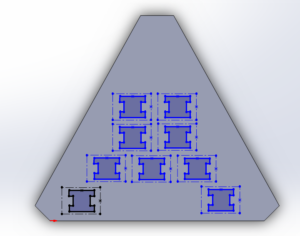
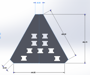
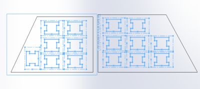
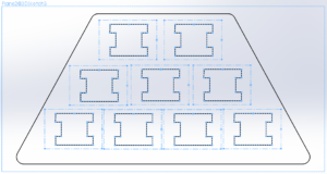
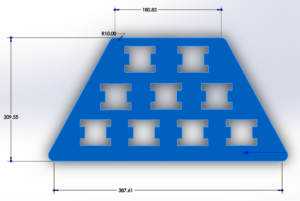
Below are the Solar Array Panels that were created using Solidworks 2018. A google drive link is also provided here.
Verification & Validation Test Plan
By: Eduardo Charcas & David Born
Click on the following link to access V&V Test Plan
Concluding Thoughts and Future Work
By: David Born
In the next generation, the PCBs on the solar cells should use only SMD parts, which may mean that ethernet cables should not be used. Since mechanical engineering resources are not available to electrical engineers, the articulation and panels fabrication should be left for last so as not to distract from the main task of providing power to the battery.
References/Resources
These are the starting resource files for the next generation of robots. All documentation shall be uploaded, linked to, and archived in to the Arxterra Google Drive. The “Resource” section includes links to the following material.
- Project Video
- CDR (PowerPoint, Prezi, or PDF)
- PDR (PowerPoint, Prezi, or PDF)
- Project Libre (with Excel Burndown file) or Microsoft Project File
- Verification and Validation Plan
- Solidworks File (zip folder) Linked to in Mechanical Design Post
- EagleCAD files (zip folder) Linked to in Electronics Design Blog Post
- Arduino and/or C++ Code (zip folder)
- Other Application Programs (Processing, MatLab, LTSpice, Simulink, etc.)
- Complete Bill of Materials (BOM) with vendor names for both mechanical and electrical parts. Create in Excel or your favorite spreadsheet application. Upload as PDF. Do not post receipts, which may contain sensitive information including your name, address, and credit card information. Do not simply draw a black box over material in Word. Hackers can easily remove!
- CSULB Innovation Space (I-Space)
- Fall 2018 Solar Array Amperage Testing
- Fall 2018 Schedule

