Pathfinder Solar Array Fall 2018
Solar Panel PCB EAGLE Designs
Author/s: David Born
Table of Contents
Introduction
The old design had too many problems with connections and looked ugly so there was a new requirement to streamline the design and secure the connections between the solar cells. The main advantage of the new design is to utilize the bottom of the aluminium panels. RJ45 female Ethernet headers were chosen to be put on the PCBs because they are inexpensive and easily available. The Cat 5 Ethernet cables used in the RJ45 headers are typically AWG24 and thus can support up to 3.5 Amps before melting1. The basic unit of three solar cells in series will hereafter be known as a module. Each module will have two cells with Voltage PCBs and one cell with a Current Node PCB. A Power Hub PCB was designed to combine the power of all the cells before sending to the battery.
Solar Panel Module PCBs
Ethernet cords will be used to link the cells in series to form modules and then in parallel to get the desired current. Figure 1 shows an example schematic of the tail modules hooked up as previously mentioned. All of the cell PCBs will have solder points to connect the power generated from the cell to the board. The trace width on the PCBs are 10mil. As shown in figure 2 from an online trace width calculator2, the trace width is approximately big enough to support the 0.75mA max current expected in the cells. The Current Node PCBs will have an AtTiny, an INA169 current sensor, and three RJ45 ethernet headers (see figures 3 thru 6). The INA169 schematic design was from Adafruit3 but to minimize the size of the PCB the sensor parts were bought individually and assembled into a smaller board design. The AtTiny EAGLE schematic was downloaded from Autodesk Eagle4 AVR-7.lbr library. The boards have top layer copper plating connected to VCC and bottom layer plating connected to GND (see figures 5 and 6). The top layer also has a GND copper plating located on the top left of the board (see figure 5) in order to minimize the potential resistance from small traces on the GND line.
The Voltage PCBs will use the same designs as the Current Node Boards but will only be populated with a 0 ohm resister instead the current shunt resister and two RJ45 ethernet headers.
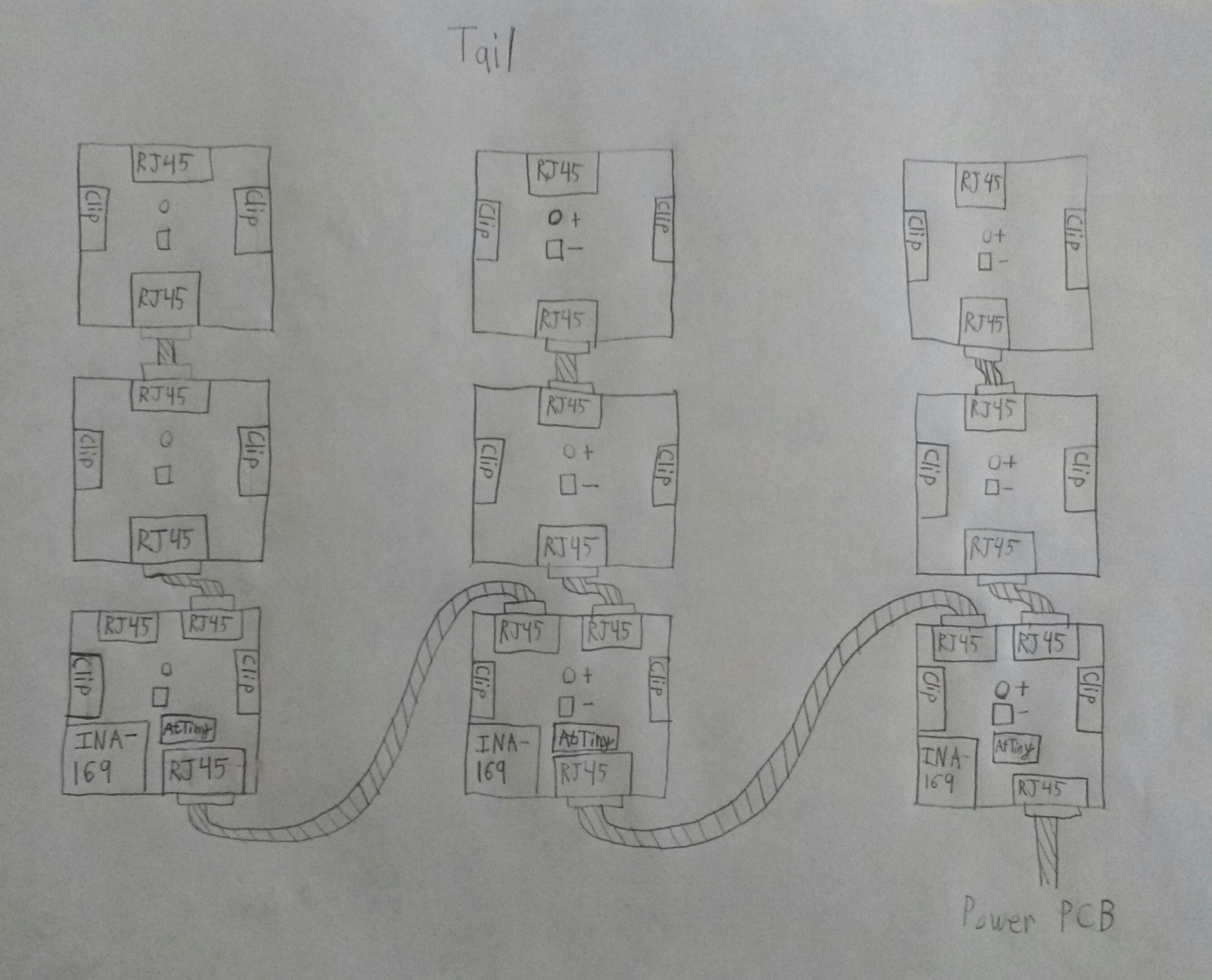
Figure 1: Example of Module Connections for Tail
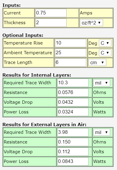
Figure 2: Trace Width Calculations
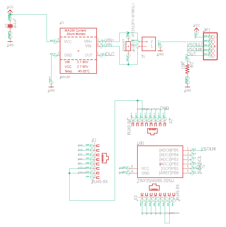
Figure 3: Current Node PCB Schematic
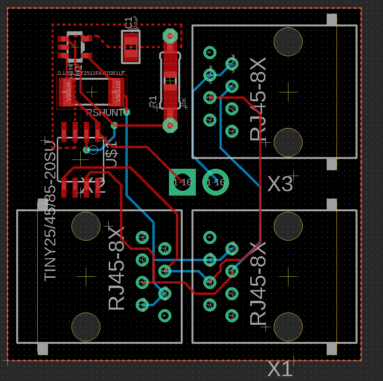
Figure 4: Current Node PCB Board Layout
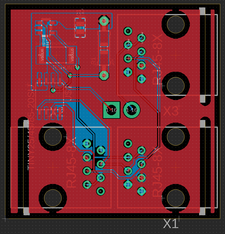
Figure 5: Current Node PCB Top Layer Copper Plating
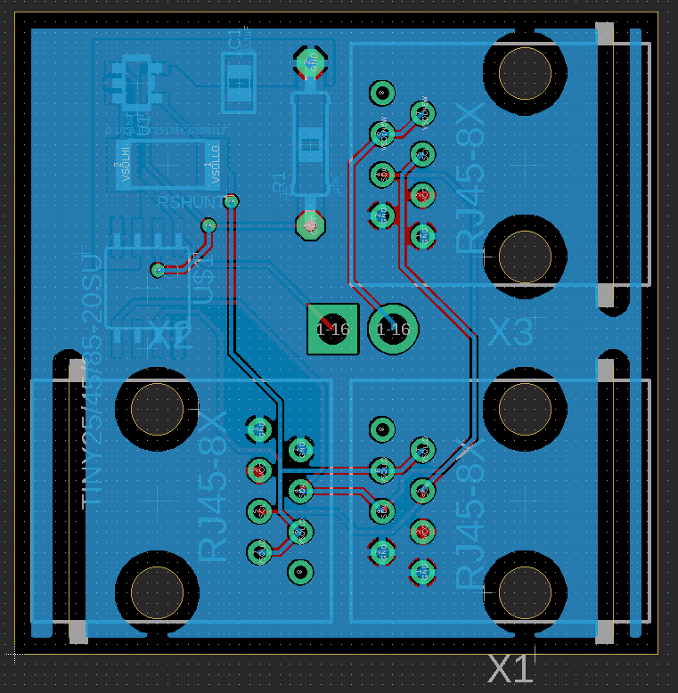
Figure 6: Current Node PCB Bottom Layer Copper Plating
Power PCB
The Power Hub PCB will have four RJ45 ethernet headers and will have holes for power transfer to and from the Arduino Uno board and the DC regulator used to charge the battery (See figures 7 thru 9). The VSOL hole in the EAGLE file will be wired to the DC regulator while the other 4 holes (SDA, SCL, GND, and VCC) are to be wired to the Arduino Uno. Each RJ45 header connects to a module from a section of the solar array such as a wing, tail, or main plate section (See figure 1). The Power PCB has copper plating connecting to VCC on the top and GND on the bottom.
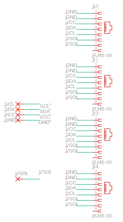
Figure 7: Power PCB Schematic
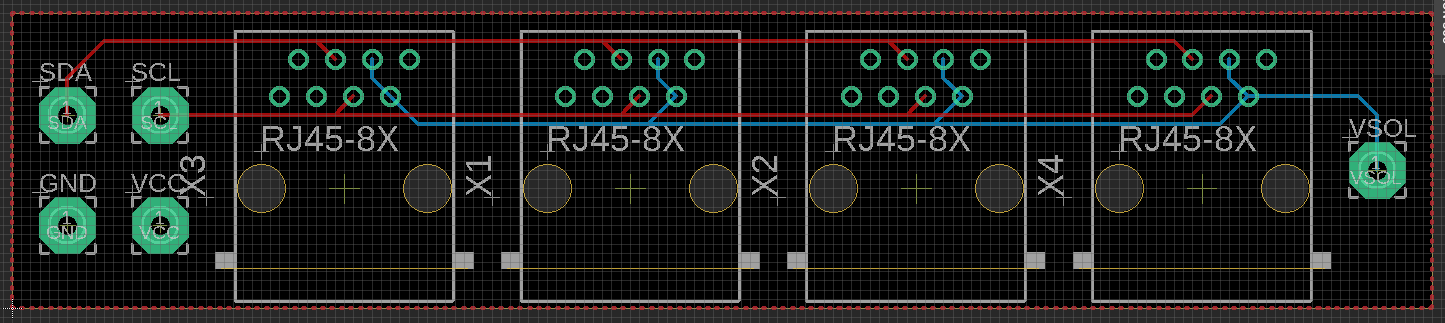
Figure 8: Power Board PCB Board
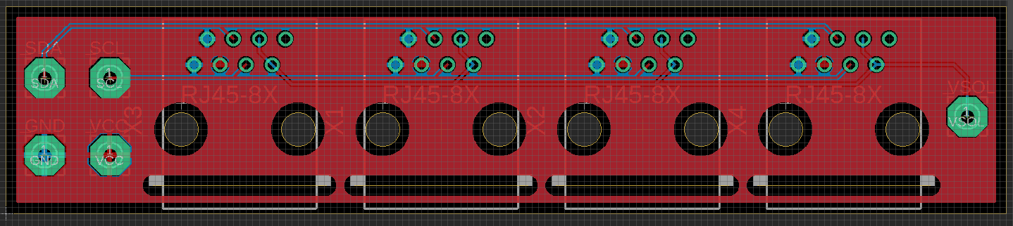
Figure 9: Power Board PCB Board Top Copper
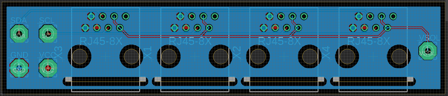
Figure 10: Power Board PCB Board Bottom Copper
Conclusion
The Current Node and Voltage PCBs ended up being 1575mil by 1575mil, or 4.0005cm2. Small hooks to hold each cell in place are currently being designed. The power PCB ended up being a 9.9cm by 2.1 cm. The copper plating was an interesting concept to minimize the number of traces on the PCB. Since these PCBs don’t have a lot of components, the traces do not have to be as carefully place to avoid choking the plate paths. On some complex PCBs, multiple plates are placed on sections that require less resistance or are have solderpads that are supposed that are on the opposite side of the desired charged plate.