Load Switch
Introduction
One of the features that MarioBot should be capable of doing is to temporarily increase it’s nominal speed rating based on the class that was originally chosen prior to starting the race. In order to achieve this feature, a Top Shield was created, such that our goal could be completed.
Schematic Design
To make our schematic as simple as possible, we looked into various sections within our circuit that could potentially be replaced with a single integrated circuit (IC). Using the Mod Wheels Gen 3 project as a reference for our boost mechanism, we noticed that the high side switch that was used in their design, shown in Figure 1, could be replaced by the ITS4142N, which is more commonly known as a high side load/power switch.
The high side switch works in a way in which it consists of two important components: an NPN bipolar transistor and a P channel MOSFET. An input signal, which comes from the 3DoT board, will be connected to the base terminal of the NPN transistor. The collector terminal of the transistor will then be tied to the gate of the P channel MOSFET and the emitter of the bipolar transistor will be connected to ground. Based on the input signal (HIGH/LOW), this configuration of transistors will ultimately act as a switch. When this switch is closed (3DoT signal HIGH), the supercapacitor will now be connected to the line that the motors are connected to, denoted as 5V_VM. To confirm the design of Figure 1, Figure 2 shows the circuit that was constructed for validation.
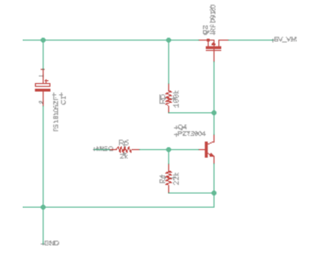
Figure 1. Mod Wheels Configuration
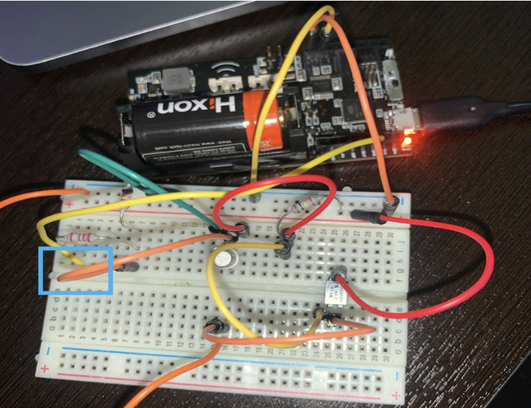
Figure 2. Breadboard Test of ModWheels Gen. 3 High Side Switch
The Arduino code that was used to test this breadboard configuration was fairly simple, as shown in Figure 3. Essentially, pin 12 from the 3DoT board was defined as an output, to where it will toggle between a HIGH signal and a LOW signal every 5 seconds.
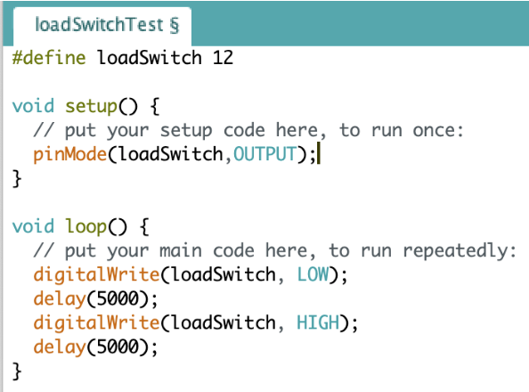
Figure 3. Arduino Code to Validate High Side Switch
To validate the circuit, connecting pin 12 from the 3DoT to the input terminal of the High Side Switch, which is the yellow wire within the blue box of Figure 2, will trigger the switch, thus changing the voltage based on the supply value. This test was verified using a multimeter. Verifying this design even further, we created an LTSpice circuit model, as shown in Figure 4, where the High Side Switch configuration was simulated using a switch component as denoted by S1. In this model, a zener diode was used such that the diode will only allow current to flow in one direction. Without these diodes, the circuitry outside the scope of this boost mechanism design would not be able to handle the voltage that we are intending to use for the motors. In addition, the supercapacitor was also connected to this model, denoted as C1, so that we can simulate the charge and discharge rate. Simulating this circuit shows that 12 volts is going to the motors only when the switch is set to high, which was ultimately what our goal was. This simulation as well as the previous tests have provided enough confidence for the MarioBot team to continue on with this project.
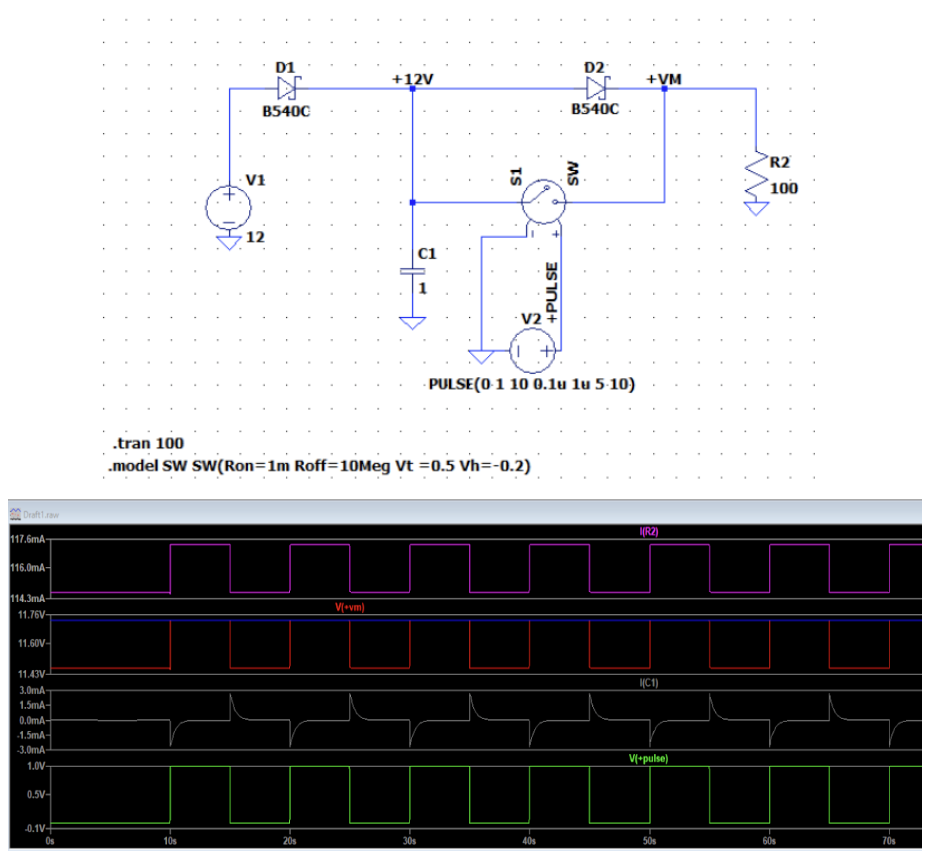
Figure 4. LTSpice High Side Switch Circuit Model and Simulation
To build off upon, or improve our implementation of the ModWheels Generation 3 design, utilizing the ITS4142N was the route that we went towards. Shown in Figure 5 is our implementation of the new Load Switch that will be in place of the previous design and Figure 6 shows the footprint and pinout of the IC chip as well. It is important to note that the signal that originates from the 3DoT board will be connected to pin 3, denoted as LoadSwitch.
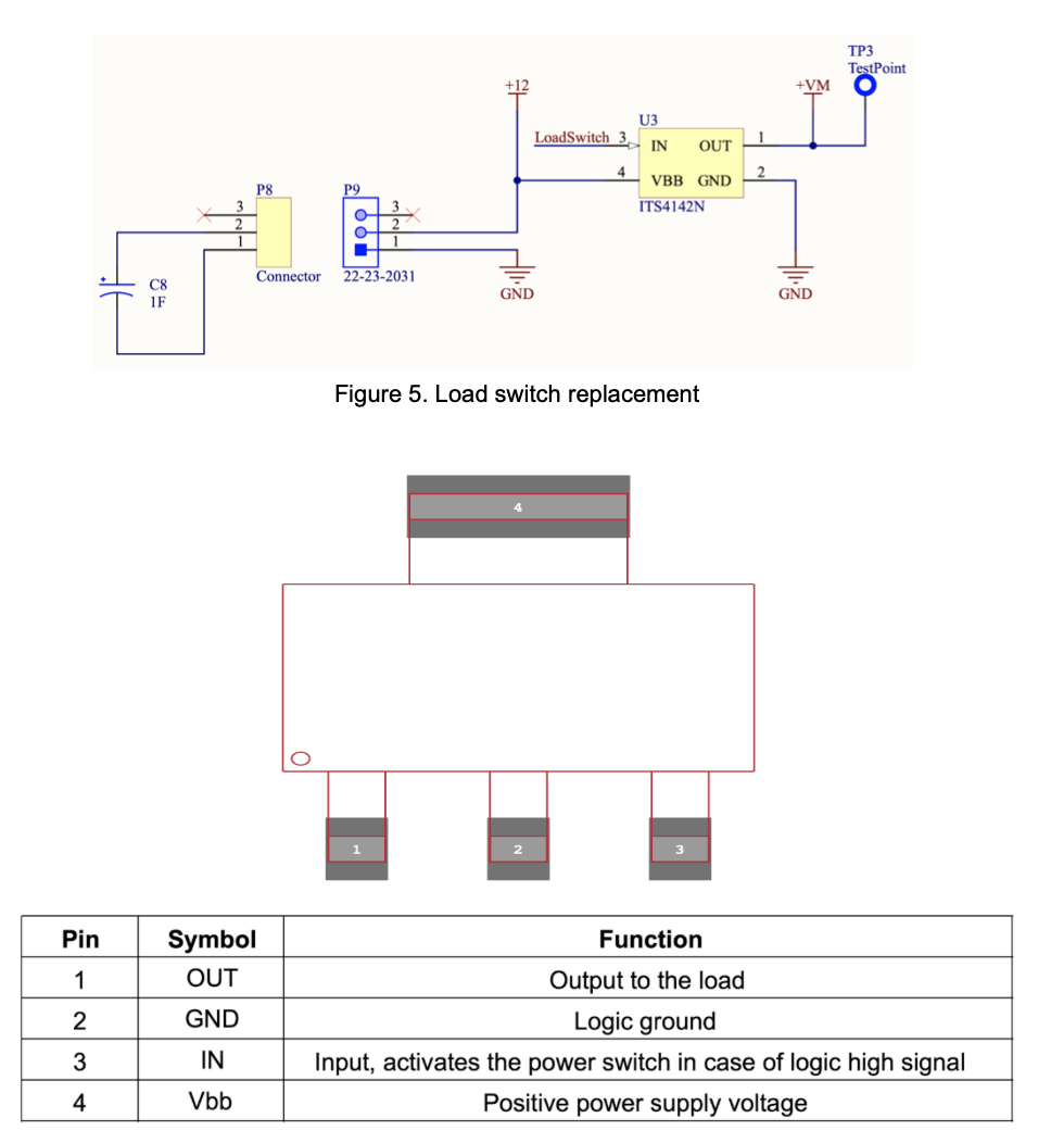
Figure 6. Footprint and Pinout of ITS4142N
Another breadboard test was done to verify our design, as shown in Figure 7. Here, the ITS4142N, denoted in the blue box, is connected to a commercial boost converter that will increase the 3.3V from the 3DoT board to the 12V that we want. With the same code from Figure 3 being implemented, the Load Switch is performing just as we expected, where based on the input state from pin 12, the voltage reading from the multimeter would increase to 12V, or drop back down to the original voltage of 3V.
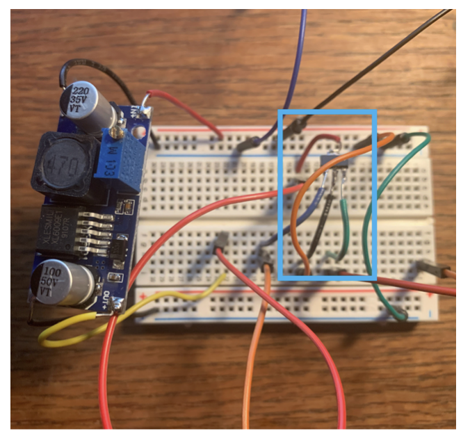
Figure 7. Load Switch and Boost Converter Test
Conclusion
The ITS4142N Load Switch was an innovative improvement to the boosting mechanisms that have been used in previous designs. Not only is it one less section of a design to worry about, it also creates a more efficient circuit, since the ITS4142N provides various advantages such as overload and short circuit protection.
