Dragonbot/Spring/2021
LDC Front Shield PCB Board Design
Author: Muath Almandhari
Table of Contents
Introduction
This research will go over the steps and processes that were taken in designing the PCB front shield of Dragonbot. The shield will be containing two LDC IC chips which will control three LDC channels coil antennas. All three channel coil antennas will be mounted on the front of Dragonbot’s chassis and connected to their corresponding LDC IC.
LDC PCB Design Research
In order to make Dragonbot able to stay within the path and do not deviate into the boundaries as well as to identify rooms and intersections, Dragonbot would need to use three LDC sensors that are placed on the right, left, and front of it. However, due to Dragonbot’s construction design which requires switching between the front and the back, the front shield’s antennas will be jump wired from the front to the back of the robot with the same antenna placements.
LDC PCB Requirements
By testing the LDC using Arduino UNO and Grove Base Shield, I realized that LDC requires only a few number pins to be used. LDC sensors only require SDA and SCL pins which are important for I2C serial communication, power pin which is 3.3V, and GND pin.
Because Dragonbot will be using the caster which was planned to be placed on the front side of the robot, there were some design limitations required for the front shield. The front shield dimensions were limited to be about 1.5” * 1” or less. As a result, it was necessary to come up with a solution that would help to reduce the size of the shield. Testing the LDC sensors help me to learn how to program and use two channels connected to one IC. Therefore, I decided to connect two channels in one LDC IC and one channel on the other LDC IC.
Constraints
- The dimensions of the front shield must be limited to 1.5’’ by 1’’ or less due to space limitations.
- Since the PCB board will be ordered from OshPark.com, then the PCB design must have no errors in both ERC and DRC tests using the specified by OshPark DRC EagleCAD files in order to meet their manufacturing standards.
- The PCB design must be approved by Professor Hill before April 4th in order to have the time to order the right components, solder them, and finally test the board
Iterations
Since PCB front shield designing was a learning process for me, I had to do multiple revisions for my designs in order to get the instructor’s approval. Therefore, it was an iterative process that was done in three itterations.
First Iteration
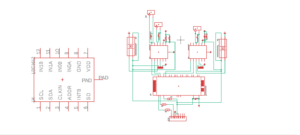
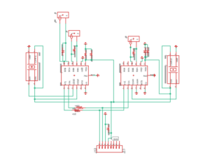
After analyzing the LDC circuit and proving that it works as it was intended, I started to design my LDC PCB front shield. Therefore, I started with design a schematic that contains two LDC sensors which one of them will have two channels and the other one will have one channel only. Then, I connected SDA and SCL to the head connectors in order to be connected to the 3Dot board. In addition, I connected jumpers to pin ADDR in order to make each IC handle more than one address. Furthermore, I connected a connected an external oscillator to pin CLKIN in order to improve the LDC measurements. Finally, I connected both LDC ICs to a multiplexer in order to be able to control both LDCs at the same time.
However, after restudying the datasheet again, I realized that this connection could be more simplified. I learned that I could assign each LDC IC to a specific address by connecting the ADDR pin to either GND or 3.3V. When ADDR is connected to low, I2C address will be 0x2A; however, when ADDR is high, the I2C address will be 0x2B. This helped me control the address of each LDC IC and get rid of the multiplexer. Furthermore, since each LDC IC is assigned to a specific address, I was also able to get rid of the jumpers that were connected to the CLKIN pin because it will not require changing addresses between 0x2A and 0x2B.
Second Iteration
After reviewing the first circuit’s schematic design with Pro. Hill and Chris and continued on looking for designing advice, we found out that I was missing pull-up resistors that were supposed to be connected to SDA and SCL pins. Therefore, I did some research and I found out that LDC1612 sensors require a pull-up resistor to high logic level. As a result, a calculated the pull-up resistors as the following:
Furthermore, Professor Hill recommended me to use the top layer as GND and the bottom layer as 3.3V in order to simplify my PCB design. Therefore, I modified my design and also did some editing on it by shortening the length of 3.3V traces and reduces the with of the traces from 13mil to 10mil. Also, I switched the communication traces from 6mil to 8mil.
Third Iteration
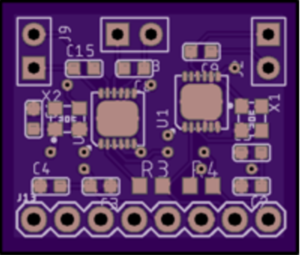
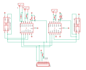
For the final iteration, I took upon Professor Hill’s recommendations and cleaned up my circuit schematic’s design by getting rid of the tangled traces. In addition, since the front shield connectors will be connected to the top shield’s, we realized that there was no need to have pull-resistors anymore because they are already connected to the RFID sensors. Therefore, I redid my circuit schematic and modified my PCB design by shortening the 3.3V traces as well as avoiding 90 degrees angle for the traces. Also, I tried to place the capacitors as close as possible to the head connectors in order to charge power the most and to reduce the dimensions of the PCB board to be 0.75” * 0.9”.
PCB Ordering
After finishing my third PCB board revision and getting my approval from Pro. Hill, I went ahead and ordered my PCB fabricated boards. I ordered my PCB boards from OshPark.com because it is relatively cheap and very quick in terms of making simply fabricated PCB boards.
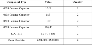
Furthermore, I started ordering my passive components and LDC IC’s that will be used for the PCB board. Thus, I ordered my parts from both Digi-key.com and Mouser.com. The table below shows the components used for the LDC PCB board.
PCB Soldering
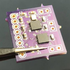
Once I got my PCB fabricated board and the components mailed, I started my next step which is soldering the parts into the board. Therefore, I used a low-temperature soldering paste because it is very simple to use and easier for soldering surface mount components for bigger. I applied the soldering paste into the desired pins to be connected and placed the components into their proper positions at their proper orientations.
The next step was to apply heat to the PCB board in order to milt the soler paste and connect the components. For this step, I used a hot pan and controlled its temperature to 120 Celsius by using a thermometer. One of the main downsides of using a soldering paste is that it can create solder bridges between the IC pins which would make them short. I was able to solve this problem by using soldering iron and applying it to the pins of the IC.
Conclusion
PCB designing was a very beneficial and helpful assignment. I have learned a lot from the instructor’s advice on how to create my own fabricated circuit board and how to customize it. I learned about how to make use of the layers to simplify my PCB design and what traces should be used for each specified pin. I also learned the process of how to build one and how to fix common problems they would have.

