ATmega Analog-to-Digital Conversion
Table of Contents
Reference(s):
- The AVR Microcontroller and Embedded Systems using Assembly and C by
Muhammad Ali Mazidi, Sarmad Naimi, and Sepehr Naimi, Chapter 13 ADC, DAC, and Sensor Interfacing - ATMEL 8-bit AVR Microcontroller with 4/8/16/32K Bytes In-System Programmable Flash, Chapter 23 “Analog-to-Digital Converter”
- AVR Freaks Newbie’s Guide to the AVR ADC by Ken Worster
- Successive Approximation ADC, Georgia State University, Department of Physics and Astronomy
- Successive approximation ADC, Wikipedia
ATmega MCU ADC Subsystem Features
- 10/8-bit Resolution
- 0.5 LSB Integral Non-linearity
- ± 2 LSB Absolute Accuracy
- Temperature sensor
- Single Conversion, Free Running, and 3DoT Mode 8
- Interrupt on ADC Conversion Complete
- Optional Left Adjustment for ADC Result Readout
- 2.56 V ADC Reference Voltage
- Up to 15 kSPS at Maximum Resolution with a conversion times of 13 μs (ATmega328P) and 65 – 260 μs (ATmega32U4)
- Six (ATmega328P), twelve (ATmega32U4), and five (3DoT) Multiplexed Single-Ended Input Channels
- One Differential amplifier providing gain of 1x – 10x – 40x – 200x (ATmega32U4 only)
- Sleep Mode Noise Canceler (ATmega32U4 only)
How it Works
What is a Successive Approximation ADC?
Illustrations from Tocci, Ronald J., Digital Systems, 5th Ed, Prentice-Hall, 1991.
A successive approximation ADC is a type of analog-to-digital converter that converts a continuous analog waveform into a discrete digital representation via a binary search through all possible quantization levels before finally converging upon a digital output for each conversion.
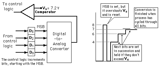
The successive approximation Analog to digital converter circuit typically consists of four chief subcircuits. Figure 1 is an example 4-bit ADC and will be used to illuminate how these four subcircuits work together to convert an analog value into a digital number.
- A sample & hold comparator circuit acquires the analog input voltage (Vs) and compares it to the output of an internal DAC with input reference voltage (Vref). To keep the illustration as simple as possible, this reference voltage is not shown and may be assumed to be equal to 15 v. In our example 4-bit DAC the analog input voltage (Vs) is set to 7.2 volts.
- The result of the comparison is sent to a successive approximation register (SAR). Identified as control logic and bits D3 to D0 in our simplified 4-bit DAC block diagram.
- The internal DAC supplies the comparator with an analog voltage equivalent of the digital code output of the SAR for comparison with Vs.
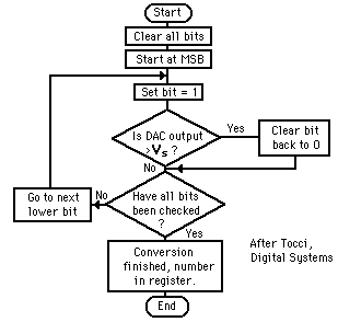
- The SAR subcircuit, a finite state machine, implements the algorithm defined in Figure
Using the Built-in ADC in the ATmega MCU
The ATmega datasheet provides everything you need to know to use the ADC subsystem of our AVR microcontroller. In the following sections I am going to focus on those topics which I consider to be most relevant when wanting to use the ADC:
- How to connect the pins related to the ADC (Voltage Reference).
- How to make an Analog to Digital conversion within the Arduino IDE.
- A Simple Analog to Digital Conversion (analogRead)
- The registers of the ADC (ADMUX, ADCSRA, and ADCH:ADCL). ADC registers ADCSRB and DIDR0 are left at default values and considered outside the scope of this introductory lesson.
- How to select an operating mode (Single Conversion and Free-Running)
- How to specify resolution/conversion speed (Sample Frequency).
- How to verify conversion complete (polling the ADSC bit).
I have tried to weave these topics into a single story centered around the ATmega32U4 and the Arduino analogRead function. Consequently, section headings are more for future reference and for the most part can be ignored if you are reading the material from beginning to end.
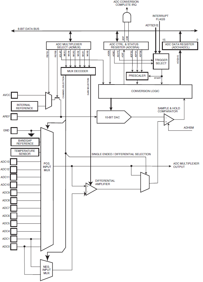
Any good story must start with the big picture and ours is no exception. In Figure 3 we have the block diagram of the ADC subsystem of the AVR microcontroller.
Note: ADCSRA ADATE signal mislabeled as ADFR in Figure 3.
Voltage Reference (VREF)
While most of our story centers around how to work with the registers of the ADC. In this section I am going to talk about how the Arduino hardware handles the reference voltage for the 10-bit DAC (AVCC to VREF), how you can improve the noise immunity of your design, and finally how you can change the reference voltage (AVCC to Vref). If you choose to do the latter, make sure you read the warning (or have a spare ATmega32U4 on hand).
The minimum value of the 10-bit output of the ADC register (0x000) represents GND and the maximum value (0x3FF) represents the voltage on the VREF line, within 1 LSB. You can think of VREF as normalizing the input voltage as defined by the following equation.
If you want to get into the details, I would recommend reading “An ADC and DAC Least Significant Bit (LSB)” by Adrian S. Nastase.
The source of the reference voltage is set by bits REFS1 and REFS0 in the ADC Multiplexer Select (ADMUX) register as defined in Table 1.
As shown in Table 1, the reference voltage to the 10-bit DAC can be sourced from an external AREF source, AVCC, or an internal 2.56V reference voltage.
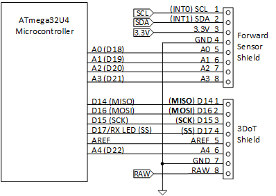
3DoT Hardware Implementation of AVCC and AREF
We are using the 3DoT board and so are limited by how they have wired these pins. Comparing this schematic with Figure 24.7.2 “ADC Power Connections” in the Reference Data Sheet of the ATmega32U4, we see that this is not the optimal wiring solution with missing 100nF capacitor from AVCC to analog ground.
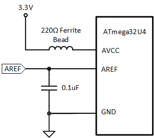
For voltage reference mode 012 and 112 (Table 1) Microchip recommends an external 0.1 uF capacitor be connected from AREF pin to analog ground to improve noise immunity. As seen in Figure 4 “How the 3DoT wires the ADC reference voltage pins” schematic, the 3DoT board comes with with a 0.1 uF capacitor to ground and a Ferrite Bead, the Arduino UNO does not come with either.
Arduino IDE Software Implementation of AVCC and AREF
The default setting for an analogRead call within the Arduino IDE sets ADMUX bits REFS1 = 0, and REFS0 = 1. Looking at Table 1 and the 3DoT schematic (Figure 4), we see that the Arduino IDE therefore defaults to a ADC reference voltage of 3.3v.
Changing the Reference Voltage
The Arduino provides a function named analogReference(uint8_t mode) which allows you to change the DEFAULT value of voltage reference source (REFS = 0b01)
void analogReference(uint8_t mode)
{
  // can't actually set the register here because the default setting
  // will connect AVCC and the AREF pin, which would cause a short if
  // there's something connected to AREF.
  analog_reference = mode;
}
Also included in the wiring.h header file are the three available values defined as constants (compare names below to Table 1).
#define EXTERNAL 0
#define DEFAULT 1
#define INTERNAL 3
For example, if you want to reference an external voltage wired to the AREF pin you would add the following code to the setup section of your Arduino sketch. In this example, AREF is wired to the 3.3 V output provided by the Arduino.
analogReference(EXTERNAL); // Vref wired to 3DoT shield AREF pin
WARNING: If you wire a voltage source directly to AREF, when the Arduino changes the ATmega32U4 default setting of 0b00 to the Arduino’s default value of 0b01, a short will exist between AVCC and AREF lines as shown in Figure 3. Even though your setup script will switch it back to its original safe 0b01 value the damage will already have been done to the ATmega32U4 (i.e., time to buy a new microcontroller). To protect the ATmega32U4 during this short period of time, add a 1K ohm resistor between your reference voltage source and the AREF pin. During normal operation the voltage drop across this resistor should be negligible.
How to make an Analog to Digital conversion within the Arduino IDE
Converting an Analog signal into its digital equivalent is accomplished within the Arduino IDE using the analogRead(pins) function. The analogRead function takes a single argument “pin”, identifying one out of the five Analog pins of the 3DoT to be read.
Using the analogRead function is demonstrated by the AnalogInput sketch (Open – Analog – AnalogInput)
/*
 Analog Input
 Demonstrates analog input by reading an analog sensor on analog pin 0 and
 turning on and off a light emitting diode(LED) connected to digital pin 13.
 The amount of time the LED will be on and off depends on
 the value obtained by analogRead().

 The circuit:
 * Potentiometer attached to analog input 0
 * center pin of the potentiometer to the analog pin
 * one side pin (either one) to ground
 * the other side pin to +5V
 * LED anode (long leg) attached to digital output 13
 * LED cathode (short leg) attached to ground

 * Note: because most Arduinos have a built-in LED attached
         to pin 13 on the board, the LED is optional.

 Created by David Cuartielles
 Modified 16 Jun 2009
 By Tom Igoe
 http://arduino.cc/en/Tutorial/AnalogInput

 */

int sensorPin = 0;   // select the input pin for the potentiometer
int ledPin = 13;     // select the pin for the LED
int sensorValue = 0; // variable to store the value coming from the sensor

void setup() {
  // set pin(s) to input and output
  pinMode(sensorPin + A0, INPUT);
  // declare the ledPin as an OUTPUT:
  pinMode(ledPin, OUTPUT);
}

void loop() {
  // read the value from the sensor:
  sensorValue = analogRead(sensorPin);
  // turn the ledPin on
  digitalWrite(ledPin, HIGH);
  // stop the program for  milliseconds:
  delay(sensorValue);
  // turn the ledPin off:
  digitalWrite(ledPin, LOW);
  // stop the program for for  milliseconds:
  delay(sensorValue);
}
In the next section we will look at how the analogRead function works. Our story is about to become a lot darker.
A Simple Analog to Digital Conversion
Before we get into the details of how the Arduino analogRead function works let me give you a thumbnail sketch of the process. If you find yourself getting lost in the forest, you may want to reread the following paragraph. Figure 5 “ADC Registers” is provided here to help you through the mnemonic soup (ADSC, ADCSRA, etc.) contained in this summary paragraph.
The Arduino analogRead function performs a simple analog conversion, where the ADC is triggered manually by setting the ADSC bit to logic one in the ADCSRA register. The ADSC bit will read as logic one as long as a conversion is in progress. When the conversion is complete, it returns to zero. The analogRead function polls this bit and returns the 10-bit result in the ADCH:ADCL register pair when conversion is complete.
Now, let’s take a look under-the-hood at the Arduino analogRead function. I am assuming the use of the Arduino compatible 3DoT board. Consequently, to simplify the explanation of this function I have removed a macro expansion required by the Arduino MEGA.
int analogRead(uint8_t pin)
{
  uint8_t low, high;

  // set the analog reference (high two bits of ADMUX) and select the
  // channel (low 4 bits). this also sets ADLAR (left-adjust result)
  // to 0 (the default).
  ADMUX = (analog_reference << 6) | (pin & 0x0f);

  // without a delay, we seem to read from the wrong channel
  //delay(1);

  // start the conversion
  sbi(ADCSRA, ADSC);

  // ADSC is cleared when the conversion finishes
  while (bit_is_set(ADCSRA, ADSC));

  // we read ADCL first; doing so locks both ADCL
  // and ADCH until ADCH is read. reading ADCL second would
  // cause the results of each conversion to be discarded,
  // as ADCL and ADCH would be locked when it completed.

  low = ADCL;
  high = ADCH;

  // combine the two bytes
  return (high << 8) | low;
}
Exercise 1: The C++ sbi instruction is now deprecated. Write one line of C++ code to replace this instruction.
The Registers of the AVR ADC Subsystem
Although the ADC subsystem of the ATmega32U4 microcontroller contains seven (7) registers (see Figure 5), only ADMUX, ADCSRA, ADCH, are ADCL are used to the configure the ADC as used by the Arduino analogRead function. We will look at ADCSRB, DIDR0 and DIDR2 shortly.
ADC Multiplexer Selection Register Initialization
Assuming the unsigned 8-bit argument pin in the analogRead(pin) function call is zero (0016), the C++ line...
ADMUX = (analog_reference << 6) | (pin & 0x0f);
...at the beginning when the Arduino bootstrap loader initializes the Analog subsystem of the ATmega32U4 microcontroller, the ADC ADMUX register is set to 0100_00002.
Let's take a closer look at each of these bits and what part they play in our story.
As originally covered in the "Voltage Reference" section of our lesson and summarized in Table 1 "Voltage Reference Selections for ADC", setting REFS1 = 0 and REFS0 = 1 means that our reference voltage VREF is equal to VCC, which we will assume is 3.3v.
The ADC generates a 10-bit result which is stored in the ADC Data Registers, ADCH and ADCL. By default, the result is presented right adjusted (ADLAR = 0), but can optionally be presented left adjusted by setting the ADLAR bit in ADMUX to logic one. For the analogRead function the result of the conversion process is right adjusted (DEFAULT value).
Exercise 2: Add unsigned 8 bit integer parameter left_adjust to the analogRead function (i.e, analogRead(uint8_t pin, uint8_t left_adjust). Use left_adjust to set or clear the ADLAR bit in ADMUX. Your function should insure all undefined bits of the ADLAR argument (bits 7 to 1) are set to zero.
Using Different Channels as seen from the Figure 3 schematics, the ADC can access multiple analog channels through the MUX. The ADMUX Register controls the MUX and the different input pins which can be directed to the sample-hold circuit. The sample-hold circuit keeps the sampled voltage level stable while the conversion is made, using successive approximation. The analogRead functions pin parameter allows the calling program to define which pin is to be read. The 3DoT board uses the ATmega32U4 processor packaged in a TQFP (See Figure 1-1 "Pinout ATmega16U4/ATmega32U4" in the data sheet). This limits us to 12 analog inputs. Of these 12 possible ADC inputs, the 3DoT makes available 5 (ADC5:ADC0). For my example, the analog signal is read on pin ADC0. Consequently, the input to the MUX is set to 0 (MUX3 = 0, MUX2 = 0, MUX1 = 0, MUX0 = 0).
ADC Control and Status Register A Initialization
During initialization (see init() subroutine in main(void)), the Arduino sets ADCSRA to 1000_01112.
The bits of the ADCSRA register are used to set the operating mode and sample frequency of the ADC. We will look at the "single conversion" and "free-running" modes of operation. These are the two most common operating modes, although there are others. For example you can program the ADC to sample an analog line at a fixed interval of time.
How to select an operating mode
Single Conversion Mode
Before starting a conversion the ADC must be enabled. This is done by setting the bit ADEN = 1 in the ADCSRA Register. As illustrated in Figure 7 this is taken care of by Arduino init() subroutine.
The ADC can be run in two modes: Single Conversion mode or Free-running mode. In Single Conversion mode the conversion is initiated manually, by setting the ADSC bit in the ADCSR Register. Arduino's analogRead function uses the single conversion mode as shown in the following inline assembly instruction.
  // start the conversion
  sbi(ADCSRA, ADSC);
Free-Running Mode
One of the disadvantages of the Arduino IDE is that we trade flexibility for simplicity. To run the ADC in Free-Running mode it may be best to make your own custom version of analogRead or to write your own ADC C++ within a more powerful IDE like Eclipse, AVR Studio, or ATMEL Studio.
Note: The Analog Comparator Multiplexer Enable ACME bit is not used by the ADC circuit and should be kept at its default value of 0.
In Free-Running mode the ADC is setup to start a new conversion immediately after the previous conversion is complete. To enable this feature, the ADC Auto Trigger Enable ADATE bit in ADCSRA (Figure 7) is set to one and ADC Auto Trigger Source ADTS[3:0] bits in ADCSRB (Figure 8) are set to zero. This selects the ADC interrupt flag ADIF as the trigger source. The ADC now operates in Free Running mode, constantly sampling and updating the ADC Data Registers.
The first conversion is started by writing a logical one to the ADSC bit in ADCSRA. If you use this mode, I would recommend enabling the I-bit in SREG and ADC Interrupt (ADIE = 1) bit in ADCSRA. Now your Interrupt Service Routine (ISR) can take action each time a conversion is complete (no more polling).
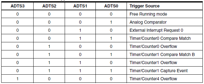
3DoT Mode 8
In addition to the free running mode, the ATmega32U4 can automatically start an ADC conversion based on a number of events, as defined in Figure 9 "ADC Auto Trigger Source Selections." Of particular interest to 3DoT robots is mode 8 "Timer/Counter4 overflow." The frequency of the PWM signal, which sets the motor speed of a 3DoT robot, is defined by Timer4. Therefore, by using this mode, a 3DoT robot can be taught to read a sensor only when it can take action (i.e., change the speed of its motors). Further, as discussed in Section 24.7.2 "Analog Noise Canceling Techniques" of the ATmega32U4 datasheet, ff any ADC port pins are used as digital outputs, it is essential that these do not switch while a conversion is in progress. Both PWM pins which drive the 3DoT motors are shared with Analog channels, by operating in Mode 8 and assuming a realistic duty cycle (motors not stalled), this restriction can be met.
How to specify resolution/conversion speed (Sample Frequency)
The sample frequency of the AVR ADC is a function of the operating mode (single conversion, free-running mode 8), the ATmega32U4 system clock frequency (CK = 8 MHz), and the prescale setting (ADCSRA bits ADPS2 to ADPS0).
From when a single conversion is initiated to the result is in the ADCH:ADCL Registers 13 ADC cycles will pass as defined in Table 2.
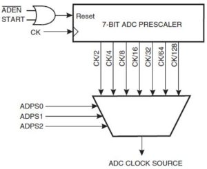
The "First conversion" line refers to when the ADEN bit in ADCSRA register is set. This additional time is required to initialize the analog circuitry including the 7-bit ADC prescaler (see Figure 10 "ADC Prescalar"). The Arduino sets the ADEN bit in the init() subroutine.
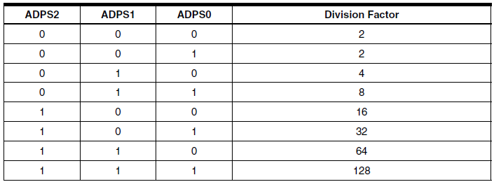
By default, the successive approximation circuitry requires an input clock frequency between 50 kHz and 200 kHz to get maximum resolution. If a lower resolution than 10 bits is acceptable, the input clock frequency to the ADC can be higher than 200 kHz to get a higher sample rate. The Arduino init() routine sets prescaler bits ADPS2 to ADPS0 in the ADCSRA Register to all ones (see Figure 7) setting the prescaler to 128. Which means that:
fADC = fCK/128 = 8 MHz/128 = 62.5 kHz
Consequently, the ADC prescaler of the ATmega32U4 generates an ADC clock frequency of 62.5 kHz (less than 200 kHz). By setting the ADC prescaler to 64 (ADPS = 0b110) we can reach a conversion frequency of 125 kHz (again less than 200 kHz), giving us a maximum resolution of 10 bits at a sample frequency of:
fsample = fADC / 13 = 9.615 ksps (104 μs Conversion Time)
This topic is covered in any number of forum posts including "How do I know the sampling frequency?"
Each conversion starts on a rising edge of the ADC clock, and at least one ADC clock cycle is lost executing code. So yes, 8928.6 Hz is the fastest you can get by calling in a tight loop, v.s. a very consistent 9615.4 Hz in free-running mode. – Edgar Bonet Nov 14 '19 at 14:46
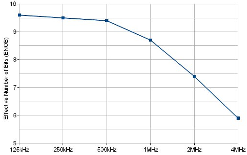
An ADC clock at 250 kHz violates the limit in ADC clocking for full 10 bit resolution (ADC clock 200 kHz for 10-bit resolution). So what would happen if we set our prescaler to divide the system clock by 32 or less? Fortunately, the "Open Music Labs" has done some in depth research and testing to answer this specific question. Table 3 "ATmega ADC resolution versus clock frequency" provides a quick answer; however, I recommend you read the article before trying this at home. From reading the article, you will discover that setting the correct bits in the DIDR register, plays a critical role in improving accuracy.
Working form Table 3, it is shown that a prescaler of eight (8) sets the ADC clock frequency to 1 MHz with a corresponding maximum sample rate of 74.074 ksps (Free-Running mode), with a resolution of an 8-bit ADC.
How to verify conversion complete (polling the ADSC bit)
When we last left our Arduino analogRead routine, it had started the analog to digital conversion process by setting the ADEN bit in the ADCSRA Register to logic one.
// start the conversion
sbi(ADCSRA, ADSC);
The analogRead routine now polls the ADSC bit in the ADCSRA register within a C++ while loop.
// ADSC is cleared when the conversion finishes
while (bit_is_set(ADCSRA, ADSC));
Once the conversion is complete, the ADC hardware subsystem of the ATmega328P clears the ADSC bit and stores the result in the ADCH:ADCL register pair.
It is important to read ADCL first to ensure that valid data is read. By reading ADCL first, the ADCL and the ADCH Registers are “locked” and cannot be updated by the ADC until the ADCH has been read.
low = ADCL;
high = ADCH;
Our story is finally over, when the high order byte is shifted 8 places to the left and or'd with the low order byte. The 10 bit answer (zero extended to 16 bits) is now returned as a positive integer (16-bit signed).
// combine the two bytes
return (high << 8) | low;
DIDRn – Digital Input Disable Register 0 and 2
Although it does not play a part in the Arduino IDE, your own design should initialize the DIDR0 register, as defined here.
When an analog signal is applied to the digital input buffer of a GPIO port pin, the buffer can consume an unnecessarily high rate of current as the input signal voltage stays within the undefined region between logic one and zero (see slew rate). To solve this problem, pins used as analog inputs should have their corresponding digital pins disabled. Specifically, set the corresponding bit in DIDRn to one. So how does this apply to the 3DoT board?
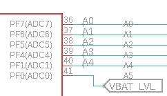
The 3DoT board can read from 1 to 6 Analog channels as defined in Figure 13 "3DoT Analog Inputs." Comparing Figures 12 and 13, it is clear that DID2 may be left at its default values (cleared). Conversely, the 3DoT board reads the battery level on ADC0D, DIDR0 bit 0. Consequently, this bit should always be initialized to logic 1. The remaining DIDR0 bits should be set or cleared based on the robot architecture.
Concluding Remarks
As we have seen, the Arduino analogRead function provides a simple way for converting an analog signal into its digital equivalent. In EE470 “Digital Control” the experimentally measured conversion time of the analog_wire_spi.ino script is 125 ?sec (sample frequency = 8 ksps). From our discussion, we know that the conversion time of our Arduino script is 104 ?sec. One thing we can take away from this finding is that over 83% of the time the script is waiting for the ADC subsystem.
Exercise 4: If you replaced the Arduino analogRead function in the analog_wire_spi script, with an interrupt driven routine and placed the ADC in Free-Running mode, what conversion time and sample frequency would you expect to achieve? Hint: see Table 2 “ADC Conversion Time.”
During our journey I hope you have also gained some insights into how we might turbo-charge the little Arduino. For example:
- Switch from Single Conversion to Free-Running mode and moving to an Interrupt driven solution, freeing the processor to do other tasks without sacrificing performance.
- Change your system clock frequency such that the ADC clock frequency can be set to 200 KHz. This will allow you to reach a sample rate of approximately 15 Kbps.
- Overclock the ADC clock to 250 kHz yielding a sample frequency of 19.231 ksps (52 μs Conversion Time).
Finally, the ADC peripheral subsystem of the ATmega32U4 provides a number of features not covered in this introductory material; not the least of which is support for differential inputs and selectable gains.
Review Questions
See Exercises included in the post.
Answers
Solutions to the exercises are to be written.

