Limbi Generation #2 Fall 2019
Limbi: Printed Circuit Board
Authors:
Alondra Vivas
Colin Rogers
Table of Contents
Introduction
This project consists of 2 separate PCBs. The PCB located within Limbi connects to the 3Dot, the pca9685 I2C chip, and the H-Bridge chips. The purpose of the PCB in Limbi is to provide the control for four additional motors that can be powered by an external source at a higher voltage than what the 3Dot can supply. This is important in order to get the torque needed to move the weight of multiple limbs. The PCB located within the modules connects to the arduino nano, the H-Bridges, and the pca9685 I2C chip. The functionality of this shield is to allow the control of four motors at once. The modules need to be able to control four separate connectors. This blog post analyses the different methods we used for bread boarding, the testing done, fritzing diagrams, schematics, EagleCAD, and ordering the PCBs. The information in the rest of this post shows the evolution of the PCBs designed for Limbi. All of the PCBs seen in this blog post were made by Colin Rogers.
Limbi Electronics
This section analyses the electrical components within Limbi. It focuses on the components that make up the different shields for Limbi. Both shields will use one Pca9685 and two L293DD chips.
3Dot
Within Limbi, we decided to use the 3Dot because of its compatibility with the ArxRobot App. It is able to control a multitude of motors, Limbi Generation #2 consists of 4 separate motors. It is also very compact to allow for it to easily fit within limb 2. The shield will connect to the SDA and SCL pins, as well has ground and 3v3.
Below shows the pinout diagram for the 3Dot.
 Loading...
Shield
The shields for both the 3Dot and the Nano Every use essentially the same components. The interface with the pca9685 I2C chip in order to get the number of pwm channels needed to run the two H-Bridge chips (l293DD). This allows for control of four motors.
Shield Components
H Bridge
An H-Bridge is a motor control chip that can be controlled by a micro-controller. The one being used here is the L293DD. It allows for the control of two motors.
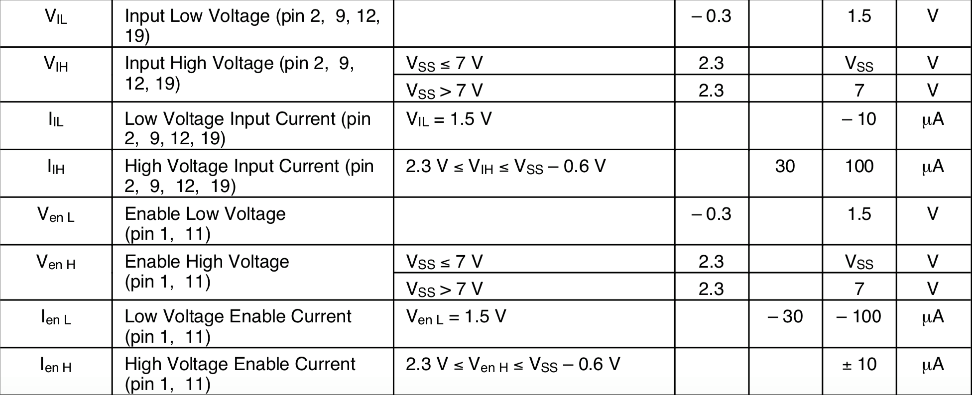
According to the datasheet shown below, an H-bridge is compatible with 3v3 logic but has to be powered with more than 4.5 v. This is important as the pca9685 uses 3v3 logic. Also, both vs and vss can go up to 36v which is why both are running at 7.4v. The reason for this specific voltage is because when the motors were tested with 5v, they didn’t have adequate torque. The next easiest battery voltage available is 7.4v.
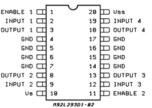
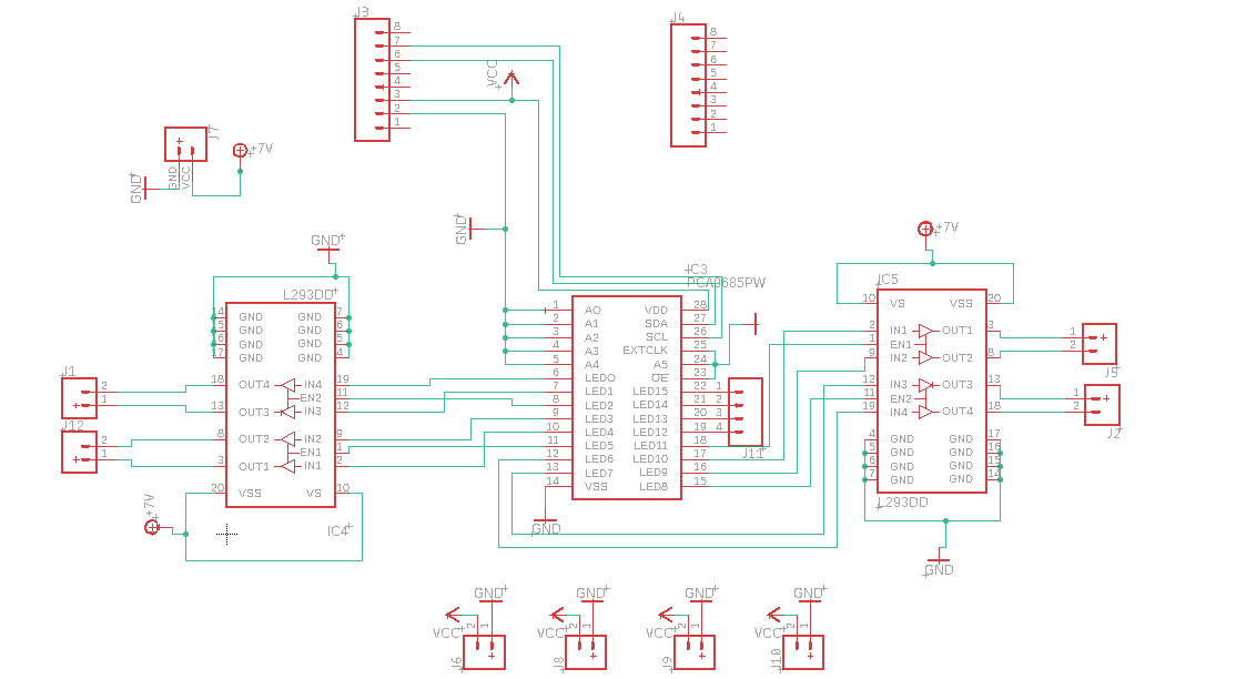
This is the pinout used by the L293DD. The output pins connect to the motors and can control two motors at a time. The input/enable pins connect to the pca9685 and allow for full control of the motors.
Pca9685 (I2C)
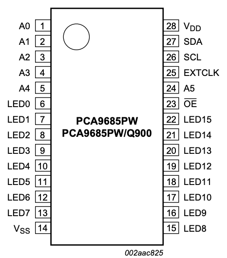
The image below shows the pinout for the pca9685 chip. It is an I2C chip that allows for the control of 16 separate pwm channels. Two entire H-Bridge chips can be controlled, which allows for the full control of four distinct motors. Limbi Generation #2 is using a micro gear motor in each of its 4 joints. The important pins here are the LED pins. These are the pwm channels that are used to control the H-Bridge motor control chips. The SCL and SDA pins allow for serial communication to the 3Dot.
HM-11
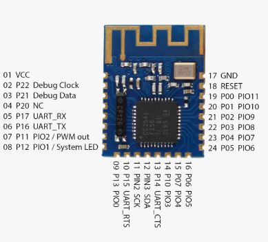
Below is the HM-11 bluetooth module and its pin out. It’s connected to 3Dot via the Tx and Rx pins. It’s not part of the shield, but it’s an integral part of controlling Limbi. This allows for wireless serial communications between the Arxterra App and the micro controller. The module that was attached to the bottom of the 3Dot was having connectivity issues; therefore, a new module was wired directly to the Tx and Rx pins. This module was chosen for its compatibility with the app and the 3Dot.
Schematic
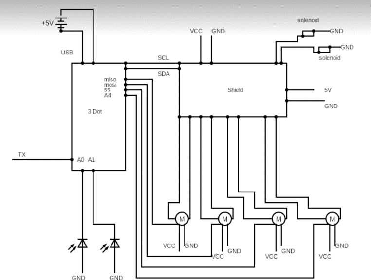
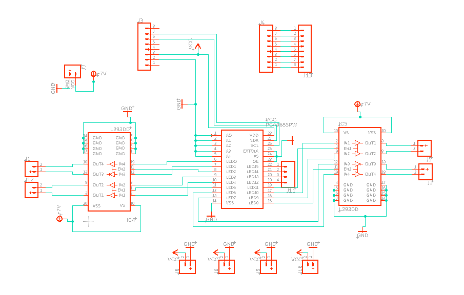
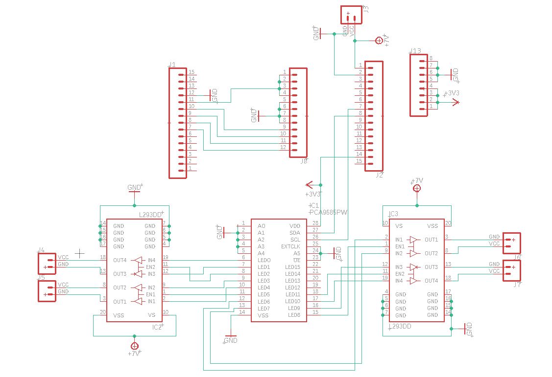
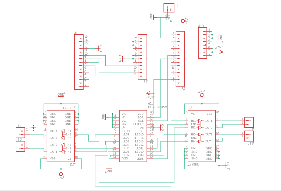
The schematic down below show the basic idea of what Limbi’s shield will need to perform. It shows that it needs to be able to control four motors.
General Iteration
EagleCAD V1
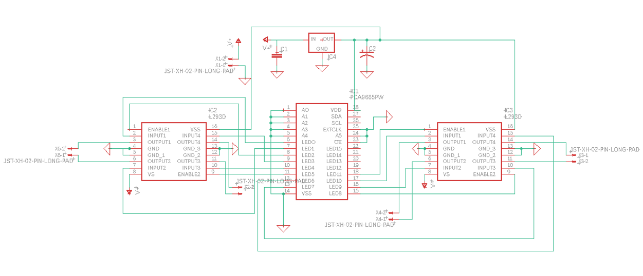
Schematic
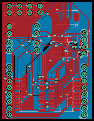
This is the V1 design for the shield. It still uses the L293D variant of the H-bridge which is a larger through-board version of the L293DD. Another thing to note is that it had a built in 5 volt voltage regulator to power the H-Bridge chips. This was later deemed unnecessary. The chips can be powered with voltages between 4.5v and 36v, which means that using a 5v regulator would be unnecessary. The chips can be powered with the same 7v rail as the motors.
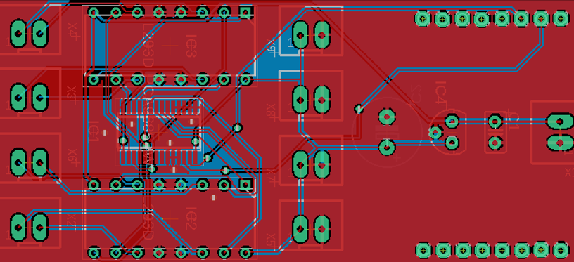
Layout
The image shown below is the V1 Eagle CAD board. It’s rather long at over 60mm. This version hasn’t adopted the star configuration for the power yet. The star configuration keeps components from being daisy chained, which would cause a larger resistance in the traces. The power traces are on the thin side and will be made thicker in later designs. The large H-Bridge chips take up more space than is necessary.
EagleCAD V2
Schematic
The second iteration of the PCB schematic is shown below. Improvements were made from previous feedback, however, for the third iteration more suggestions were given such as: add a tittle block, add filter capacitors, need connectors for the shaft encoders, too many JST connections, something larger for 7v is needed and a possibility of adding encoder signals to J8 to J11 and switching 100 mil connectors, implementation of background management, redesigning with 3dot on-board battery where a quick solution is made by replacing all the JST connectors with 100mil regulator connectors.
Layout
Board
EagleCAD V3
Schematic
Layout
Board
EagleCAD V4
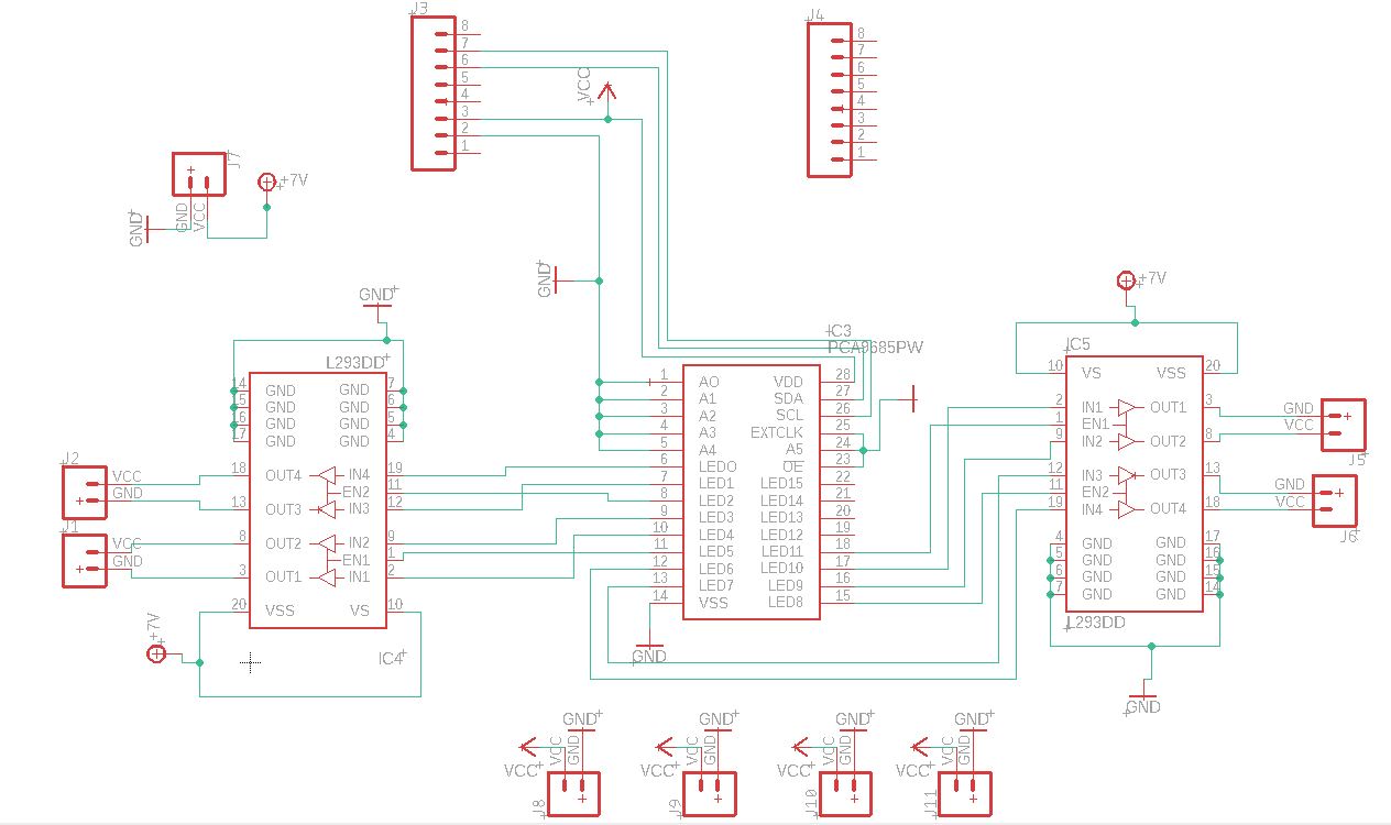
Schematic
Layout
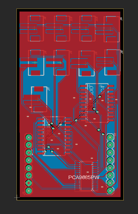
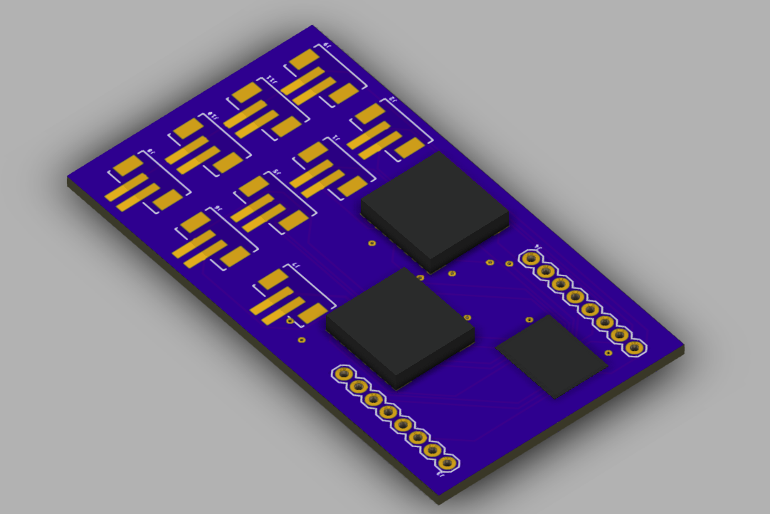
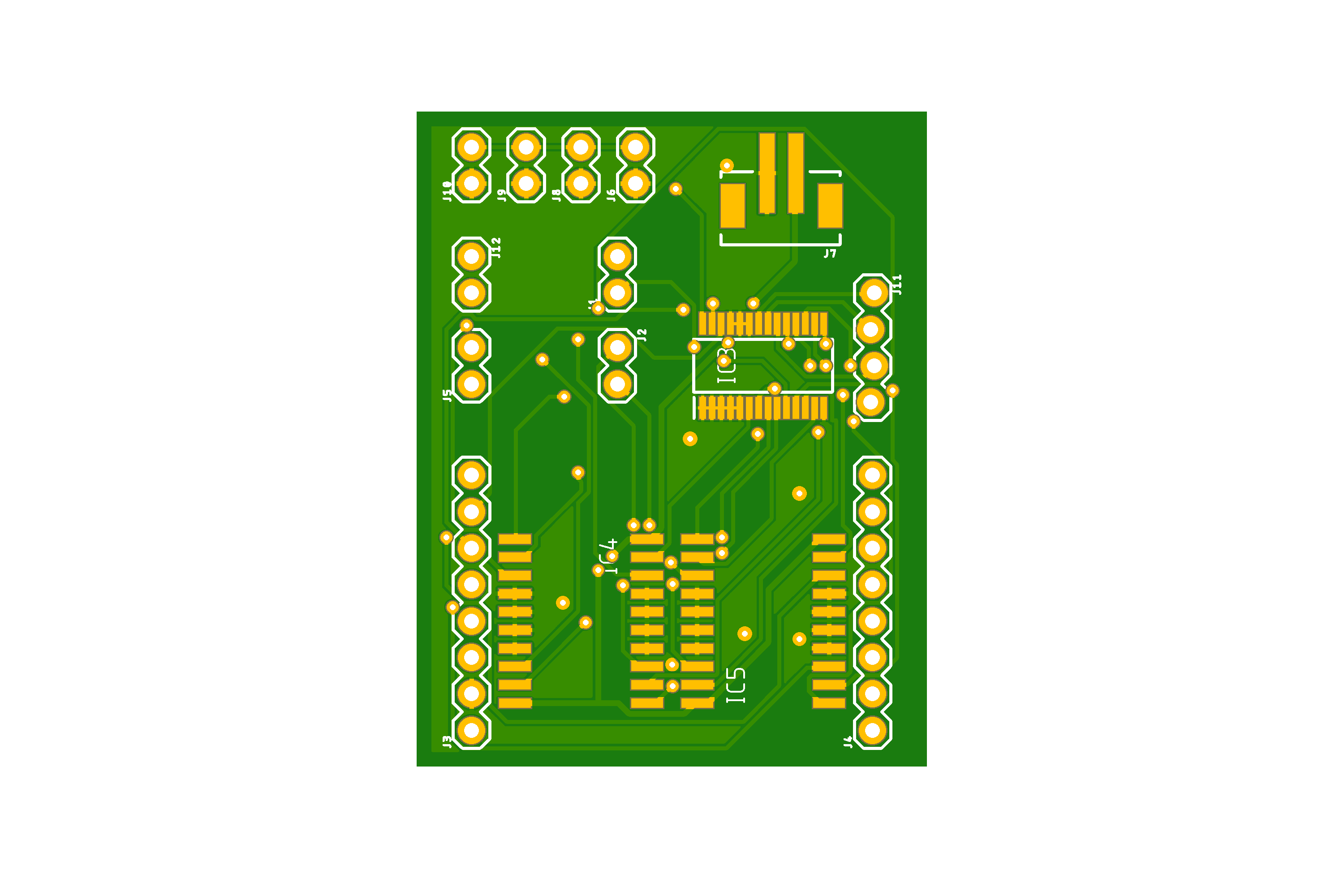
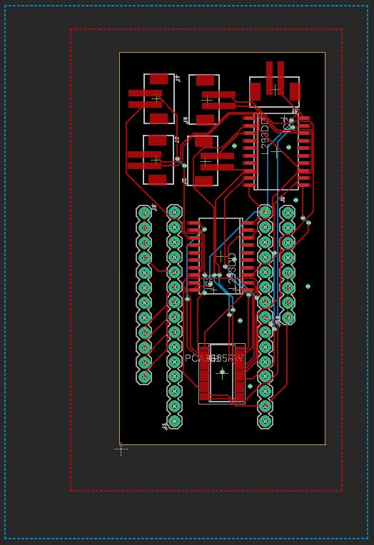
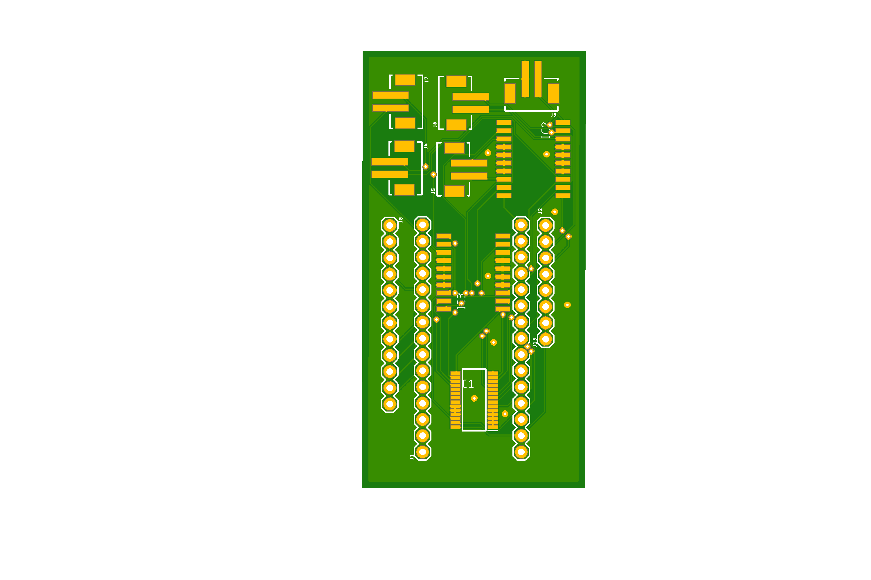
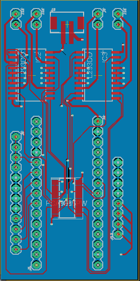
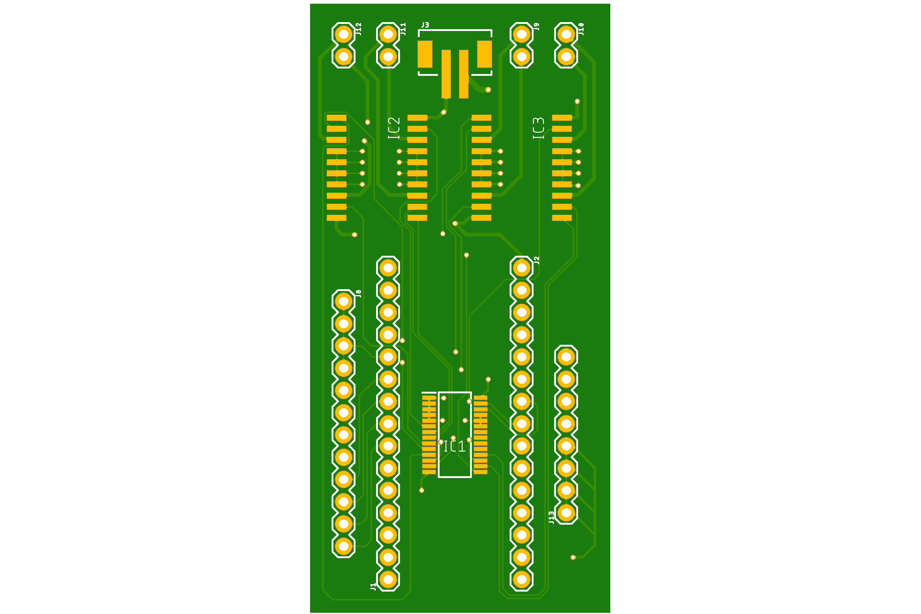
This is the V4 (final) design of the 3Dot shield. It was made slightly taller than V3 in order to accommodate the new connectors for the encoders digital inputs. It’s 48 mm long and has an improved power system overall. This shield has thick power traces, better ground routing, and the star configuration for the power. This will allow for full motor control of all joints in Limbi
Cubic Modules Electronics
The components in the modules are primarily the same except for the photo interrupters and the Arduino Nano Every.
Arduino Nano
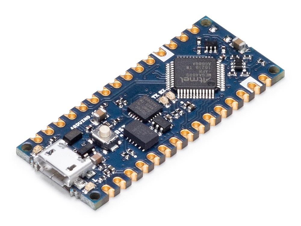
The Arduino Nano Every will be the micro controller that controls the cubic modules. It was chosen for it’s small footprint and its inexpensive cost. These boards allow the modules to communicate with the 3Dot. They will be “dumber” than the hardware in Limbi in that they will only receive commands and not give them.
EagleCAD V1
Shield
Layout
Board
EagleCAD V2
Shield
Layout
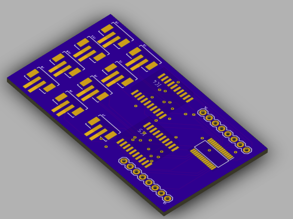
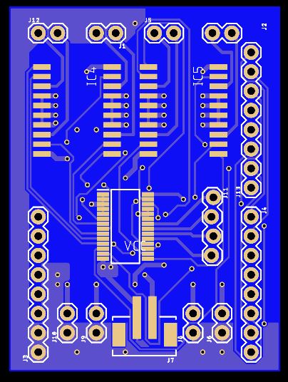
Below is the board layout for the nano every v2 shield. the big differences here are the change in connectors and a smarter power layout. It adopts the star configuration for the power like the final 3Dot board. The 2 mm connectors can be seen at the top, these were implemented to save space. This design has ground distributed on the entire bottom of the board and doesn’t have unnecessary ground planes on the top side. It’s an overall better layout which is why it was chosen as the final board.
Board
PCB Manufacturing
Once we got the approval to go forward with the manufacturer, we went to the JCL PCB website. It was confusing navigating through the webpage but we utilized the blog post by Jaap de Dood which can be found by clicking the following: JLCPCB DRC and Ordering. All in all, the process was straight forward we had an issue where we didn’t upload the Drill file with the Gerber file which caused our order to get canceled. Once we uploaded it correctly we didn’t encounter any other problems. For shipping we chose fast shipping which added to the cost. It takes 3-4 days to build, 2 days were added because we chose a blue color. If we would’ve chosen green then it would’ve taken 2 days to build. Fast shipping takes 2-4 business days.

