Pathfinder Solar Array Spring 2019
PCB Design
Author/s: Wilder Pineda (Electronics and Control)
Verification: Guitron, Brendan (Project Manager)
Approval: Guitron, Brendan (Project Manager)
Table of Contents
Introduction
When looking at the PCBs designed by the Pathfinder Generation #2 team, we came to a conclusion that their design would not function, because the sensors were receiving unregulated power from the solar panels they were meant to be measuring. The I2C traces were connect incorrectly as well. Therefore new PCB’s had to be design as well.
Passive Panel PCB
The purpose of the passive panel is to connect 3 solar cells in series to generate power for the battery. This solar panel PCB includes a 4 pin dip switch that defines its position as the middle cell or last cell in the series connection. The first 2 pins (1 and 2) define the positive side of the solar panel, pins 3 and 4 define GND. For the passive panel to be defined as passive panel 1 the dip switches would need to be set the following way (pin 1:on, pin2:off, pin3:on, pin4:off); for passive panel 2 (pin 1:off, pin2:on, pin3:off, pin4:on).
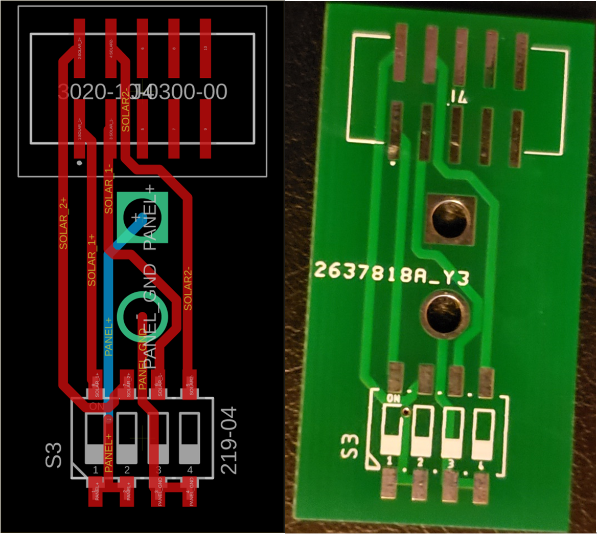
Figure 1: Passive PCB
Active Panel PCB
The Active panel PCB is soldered to a solar panel. It completes the series connection of the other two passive panels. The series connection then goes to a voltage divider which drops the voltage to a readable voltage by the ATtiny85’s ADC (PB3). This series solar voltage also goes to the INA169 which allows us to measure the current (PB4). The ATtiny85 then uses PB0 and PB2 for I2C communication (SDA and SCL). These lines travel to the bottom connector. The bottom 10 pin connector has 2 pins (which are from the 12 volt acid battery), that are used for powering the ATtiny85 and the INA169.
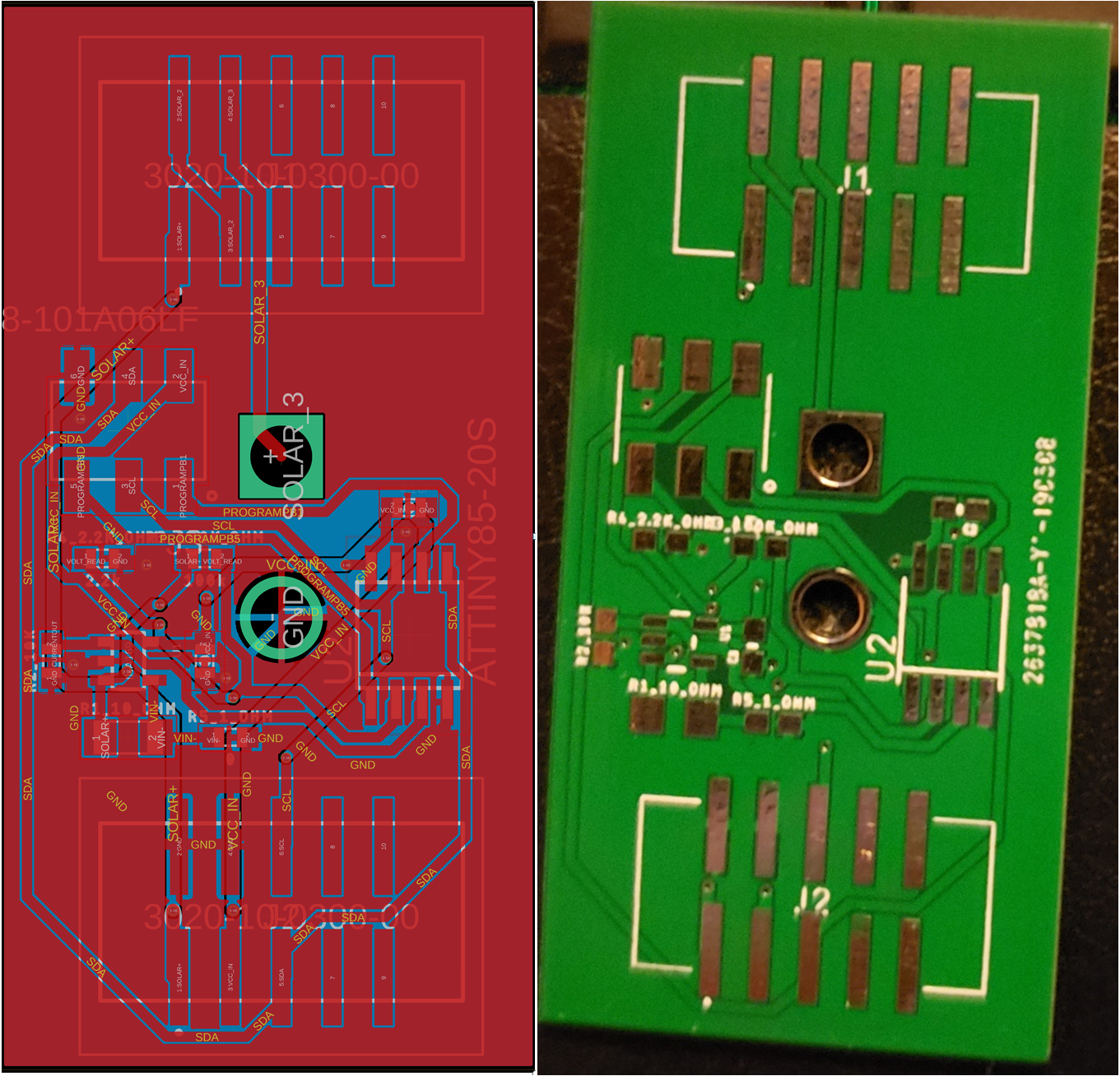
Figure 2: Active Panel PCB
Wire Bus
Each wing has its own wire bus. The wire bus allows us to connect all modules in parallel per wing. This wire bus is a long individual 10 wire, ribbon cable. The wire bus then connects to the power hub PCB.
Power Hub PCB
The power hub PCB allows us to connect 4 wire busses to it (a total of 4 wings). The power hub PCB places every module from the solar array system in parallel. It then carries the battery voltage line, solar power line, and data line to a 10 pin connector.
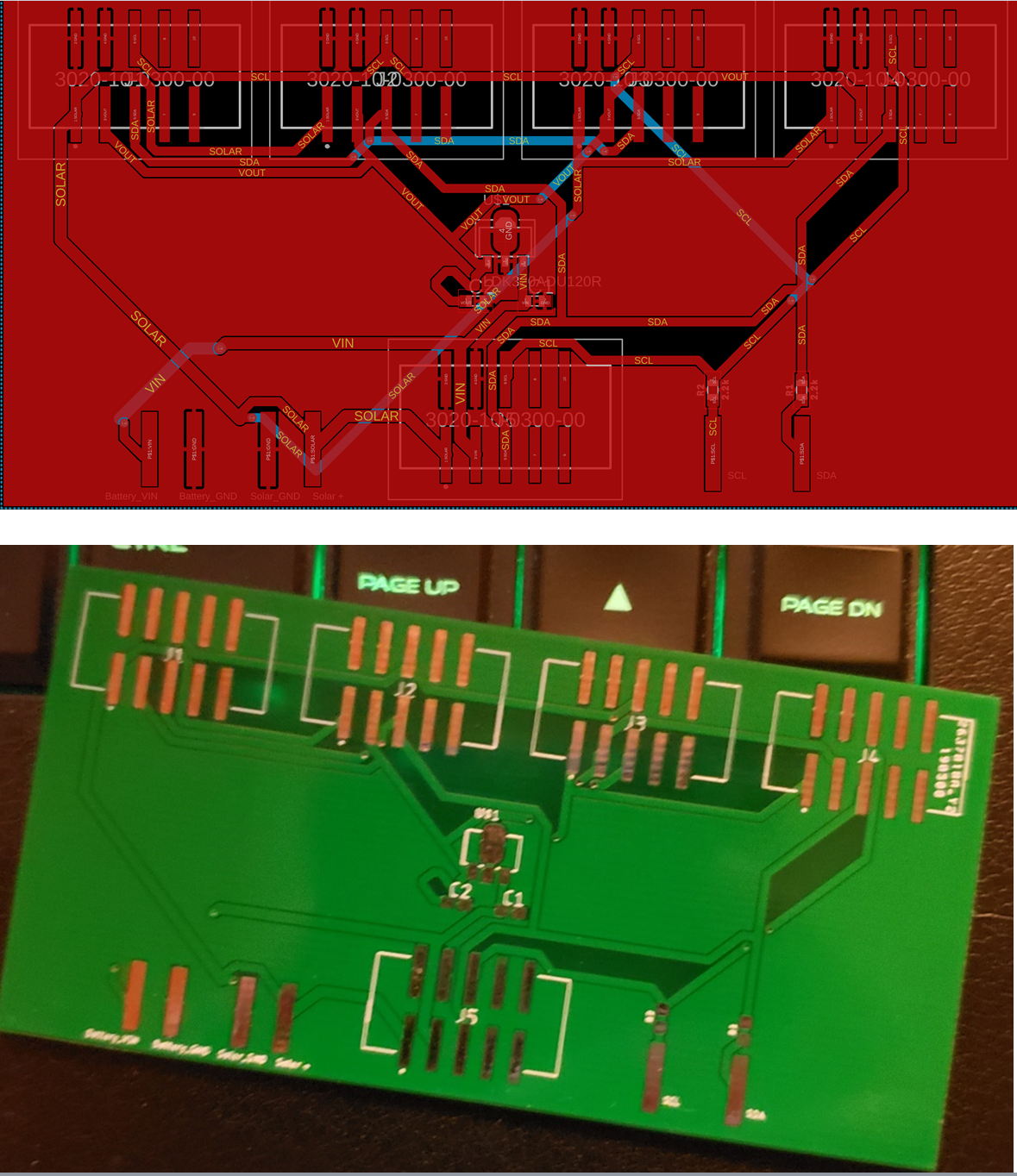
Figure 3: Power Hub PCB
Passive Panel Revisions
The passive panel went through 3 revisions first revision we were using 2 RJ45 connectors (2 different passive panel PCB’s one for passive panel 1 and different PCB for passive panel 2). Second revision we used 4 pin PST-GH connectors and the final revision was 1 ten pin connector and a dip switch as seen passive panel PCB section. (See Figure 1 for Rev 3).
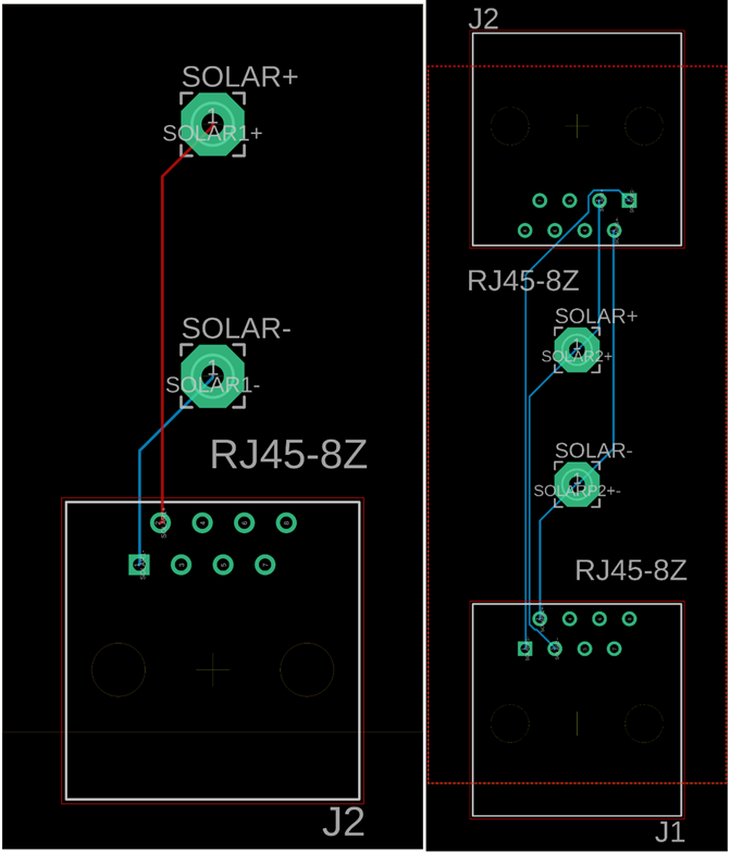
Figure 4: Passive panel rev 1 (Left image Passive Panel 1 PCB and right image Passive Panel 2 PCB)
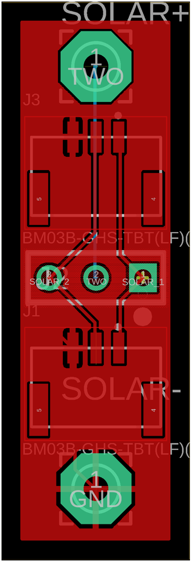
Figure 5: Passive panel rev 2
Active Panel Revisions
The first rev used Rj45 connectors. Second rev used JST-GH connectors. Third revision added connections in order to program ATtiny85 using jumper wires, and also 10 pin ribbon connectors. Rev 4 removed the ATtiny85 program connections and was replaced with a ISCP header (see Figure 2 for rev 4).
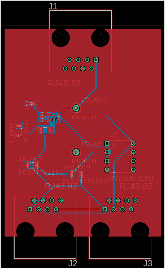
Figure 6: Active Panel PCB Revision 1
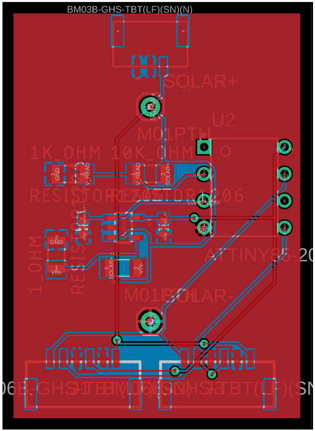
Figure 7: Active Panel PCB Revision 2
Figure 8: Active Panel PCB Revision 3