PWM Motor Speed Control using Timer/Counter 4
This article is on the motor control section of the 3DoT board using Timer/Counter 4 operating in Fast PWM mode.
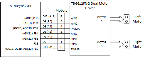
For the remainder of this article use Figure 1 “Atmega32U4 to Motor Driver Interface” to help you cross-reference the tower of babel names used by Atmel, Arduino, and Toshiba (i.e., TB6612FNG).
The direction of motors A and B are defined by inputs AIN1, AIN2, and BIN1, BIN2.
The speed of the motors A and B are controlled by changing the duty cycle of pins PWMA and PWMB respectively. With reference to Figure 1 “ATmega32U4 to Motor Driver Interface,” the speed of motor A will be controlled by Timer 4 register OC4D and motor B by Timer 4 register OC4B. The mnemonic OCnx stands for Output Compare register nx, where n is the Timer number (0, 1, 3, and 4) and x is the Compare register (Timer 4 has four (4) output compare registers designated A, B, C, and D). We will be operating our timer using “Fast Pulse Width Modulation.” I will tell you more about these registers and modes in the coming sections.
Table of Contents
Reference(s):
- The AVR Microcontroller and Embedded Systems using Assembly and C, by Muhammad Ali Mazidi, Sarmad Naimi, and Sepehr Naimi
Chapter 16: PWM Programming and DC Motor Control in AVR - ATMEL 8-bit AVR Microcontroller with 16/32K Bytes of ISP Flash and USB – ATmega32U4
Chapter 13 “8‑bit Timer/Counter 0 with PWM,” Chapter 14 “16-bit Timers/Counters,” and Chapter 15 “10-bit High Speed Timer/Counter4.”
Motor Direction Control
Figure 1 “Atmega32U4 to Motor Driver Interface” shows that we can configure 2 motors where each motor has 3 control pins and a standby (STBY) pin for the entire IC. If STBY is set low then the motors are not powered regardless of the state of the other two pins. The pins attached to AIN1/2 and BIN1/2 are digital outputs that control the rotation of the motor. The PWM inputs are connect to a pins capable of a PWM output to control the speed of the motor.
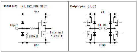
To prevent damage to the internal circuitry of the TB6612FNG, the IC includes clamping diodes on the inputs, a series resistor to limit in-rush current, and a weak pull-down resistor to keep the N-channel MOSFET OFF (Figure 2a Input Circuit). To prevent damage to the output circuitry internal flyback diodes are included (Figure 2b Flyback Diodes). Here is one of many articles on how to use a MOSFET as a Switch which goes into a little more details on these circuit elements.
The direction in which the motors turn are defined in Table 1.
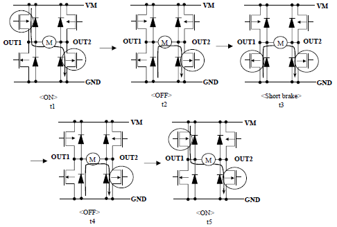
To turn clockwise (CW) you would want to set the H-Bridge to state t1 (see Figure 3 state t1). This would be accomplished by setting PD6 (AIN1) = 1 and PD4 (AIN2) = 0.
PORTD |= _BV(PD6) ;
PORTD &= ~(_BV(PD4));
For a simple “toy” brushed DC motor the magnetic field of the rotor is generated by copper wire wound around a steel-laminate core. The magnetic field is switched by a commutator located on the shaft. The stator uses fixed magnets. The rotor’s copper winding from an electrical perspective is an inductor. During normal operation the back emf generated by the rotor’s winding (an inductor) as it is switched off is routed through a flyback diode (aka flywheel, free wheeling, snubber, suppresser, catch, clamp, kick back).
When switching the motor from CW to CCW care must be taken to not short the MOSFET switches on both legs of the H-bridge while also dissipating the current generated by the collapsing magnetic fields. To solve this problem a Finite State Machine (FSM) is implemented. The controlled transition from one state to the next of the FSM is illustrated in Figure 2 “TB6612FNG H-Bridge states t1 to t5” and Figure 4 “How to program switching between states to prevent short circuit conditions.”
These figures are taken from the TB6612FNG datasheet, and it is the author’s belief that the Toshiba editors made a copy-paste error for states t4 and t5 in Figure 3.
Sample C++ Code to Configure GPIO Ports
Figure 1 is duplicated here for reference purposes.
// MOTOR PINS
// Motor A AIN1,AIN2,PWMA = PD6,4,7
DDRD |= _BV(PD7) | _BV(PD6) | _BV(PD4);      // 0xD0
// Default to low output
PORTD &= ~(_BV(PD7) | _BV(PD6) | _BV(PD4));
// Motor B BIN1,PWMB = PB5,6 and STBY = PB4
DDRB |= _BV(PB6) | _BV(PB5) | _BV(PD4);      //0x70
PORTB &= ~(_BV(PB6) | _BV(PB5 | _BV(PD4)));
// and for motor B BIN2 = PC6
DDRC |= _BV(PC6) ;                           //0x40
PORTC &= ~(_BV(PC6));
Motor Speed Control
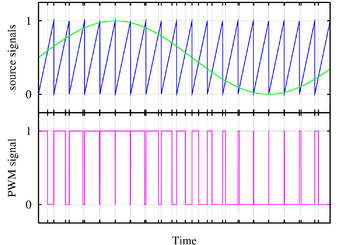
Several modulation methods have been developed for applications that require a digital representation of an analog signal. One popular and relevant scheme is pulse width modulation (PWM) in which the instantaneous amplitude of an analog signal is represented by the width of periodic rectangular wave. For example, consider the signals depicted in the figure below. Notice, the PWM version of the signal has a fixed frequency defining the point when a pulse begins. During the period of an individual pulse, the signal remains high for an amount of time proportional to the amplitude of the analog signal.
The speed of our DC motors is controlled using pulse-width-modulation (PWM). But, unlike the sinewave above, where the duty cycle changes after each cycle, we will be controlling the speed of our motors by setting a fixed duty cycle for a given speed. When the rectangular wave signal is high the motor is powered ON, and when the signal is low the power is turned OFF. The speed of the motor is controlled by the fraction of time the controlling signal is ON (duty cycle = Th/Tp %, where Th = time high and Tp = clock period).
ATmega Timer Modes
ATmega, Arduino, and 3DoT PWM Output Pins
Most microcontrollers, including the ATmega family of microcontrollers, provide at least one port that has timer sub-circuitry capable of generating PWM signals on a port pin. Typically, one just needs to configure the frequency and desired duty cycle via a couple of registers. When enabled, the port pin will output a PWM signal that can be demodulated in order to provide an approximation to an analog signal. In our design the characteristics of the motor circuit act to demodulate the PWM signal.
The Arduino Leonardo, on which the 3DoT board is based, can generate rectangular waves for PWM on digital pins 3, 5, 6, 9, 10, 11, 13. The 3DoT supports PWM signals on digital pins 3, 6, 10, 11, and 13.
ATmega32U4 Timing Subsystem
The ATmega32U4 processor has 4 timer/counter (TC) modules that can be used to generate a PWM signal. They are numbered 0, 1, 3, and 4. I will use TCx convention from now on.
Timer/Counter0 is an 8-bit Timer/Counter module, with two independent Output Compare Units, and with PWM support. The Arduino uses Timer 0 to implement the delay(), millis(), and Servo library functions.
Timer/Counter1 and Timer/Counter3 are 16-bit Timer/Counter units with three independent double-buffered Output Compare Units.
Timer/Counter4 is the only 10-bit high speed timer on the ATmega32U4 and has a lot of advanced features, including a high precision mode, double buffering (no glitches), dead time (break before make), fault protection with noise canceling (motor stall monitoring), and even support for brushless dc motors. To keep things simple we will not be using any of these features.
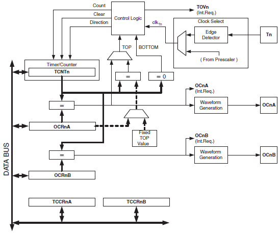
Looking at Figure 1 “ATmega32U4 to Motor Driver Interface” again we see the PWMA and PWMB are associated with OC4D and OC4B respectively. OC4X denotes an output compare with TCNT4. The ATmega32U4 has a more extensive timer system than the ATmega328P and this timer (TCNT4) has 4 Output Compare Registers OCRs attached to it. More on this subject shortly.
What is Fast Pulse Width Modulation
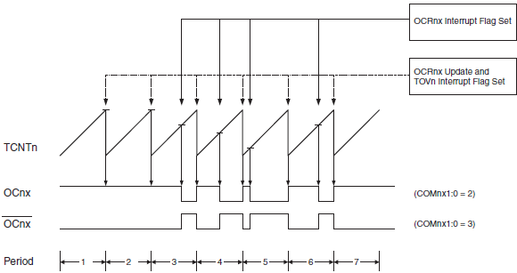
The timing diagram for the fast PWM mode is shown in Figure 15-3. The counter is incremented until the counter value matches the TOP value. The counter is then cleared at the following timer clock cycle. The TCNTn value is in the timing diagram shown as a histogram for illustrating the single-slope operation. The diagram includes the Waveform Output in non-inverted and inverted Compare Output modes. The small horizontal line marks on the TCNTn slopes represent Compare Matches between OCRnx and TCNTx. Figure 15-3 is true for Timer/Counter 4 operation. The only difference for Timer/Counters 0, 1, and 3, is the mnemonic OCWnx, which is replaced simply by OCnx.
The Timer/Counter Overflow Flag (TOVn bit) is set each time the counter reaches TOP. In fast PWM mode, the compare unit allows generation of PWM waveforms on the OCnx pins. In our case OC4D for Motor A and OC4B for Motor B.
Table 15-1 Definitions
For Timer/Counter 4 the OCR4C holds the Timer/Counter TOP value, i.e. the clear on compare match value. The Timer/Counter4 High Byte Register (TC4H) is a 2-bit register[1] that is used as a common temporary buffer to access the MSB bits of the Timer/Counter4 registers, if the 10-bit accuracy is used (Section 15.2.3 Registers). |
[1] Enhanced PWM mode adds an additional 3rd bit to the TC4H register.
PWM Output Frequency
Timer/Counter 4
For Timer/Counter 4 the PWM output frequency can be calculated by the following equation (Section 14.8.3).
I believe the equation defined in Section 15.8.2 “Fast PWM Mode” is incorrect and have replaced with equation used for calculating the frequency throughout the rest of the document.
| Equation 1.0 |
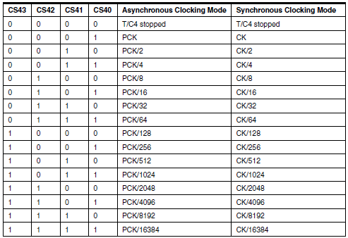
The frequency fOC4X as defined by equation 1 is a function of the system clock (8 MHz), the Prescaler, and TOP. The N variable represents the prescale divider and is defined in TCCR4B CS43:CS40 (stopped, 1, 2, 4,…16384). For our design solutions, N = 1 (no Prescaler) with the 2 bits in TC4H set to zero.,
If we want to replicate the Arduino default frequency of 31.25 kHz, then we would want to keep our TOP, defined by OCR4C, at its default value of 0xFF.
fOC4X = fCLK / 256 = 8 MHz / 256 = 31.25 KHz (approximately 32 kHz)
If we want to replicate the Adafruit Motor Shield version 1 frequency of 64kHz (62.5kHz), then we would set TOP to 0x7F.
fOC4X = fCLK / 128 = 8 MHz / 128 = 62.5 KHz (approximately 64 kHz)
If we really want 64kHz set TOP to 0x7C
fOC4X = fCLK / (1+124) = 8 MHz / 125 = 64 kHz
- At the highest range, the DRV8848 Dual H-Bridge Motor Driver does not support frequencies greater than 250kHz. Another popular motor driver the TB6612FNG does not support frequencies greater than 100kHz.
- At the lowest range, the Adafruit Motor Shield v2 operates at a frequency of 1.6 kHz, due to the limitations of the PCA9865 PWM chip. This frequency is well within the audible range and not recommended.
Calculating the PWM Duty Cycle
We will be operating our 10-bit timer/counter 4 as an 8-bit timer in Fast PWM mode.
- Frequency set by OC4C (TOP) will be defined as 0xFF = 25510
- The most significant 2-bits contained in register TC4H will always be zero.
- TCNT4 will be compared to OCR4D (Motor A) and OCR4B (Motor B).
- Therefore, the Duty Cycle = OCR4x/255, where x equals D or B
10-bit Timer/Counter 4 Register
Timer 4 is a 10-bit timer/counter. Special considerations need to be taken when writing to or reading from a 10-bit register. To write to a 10-bit register, write the most significant 2 bits to TC4H first, followed by the least significant byte (for example TCNT4). The TC4 register is shared by all 10-bit registers in Timer/Counter 4. One consequence of this common register, is that when you read a 10-bit register, the most significant 2-bits are saved to TC4H. Consequently, any subsequent 8-bit write operation to the least significant byte of a 10-bit register, will have this new TC4H value written to the high order bits. Again, this potentially unintended consequence can be avoided by always writing to TC4H first. For more on working with a 10-bit register read Atmel Document 7766 “8-bit AVR Microcontroller with16/32K Bytes of ISP Flash and USB Controller,” Section 15.11 “Accessing 10-bit Register.”
For our robots, the good news is that we never read a 10-bit register. Specifically, the Timer/Counter4 high byte (TC4H) will be always be kept at its default value of zero (0x00).
If you were wondering, TC410 (Bit 2) is an “optional” accuracy bit for 11-bit accesses in Enhanced PWM mode. The enhanced PWM mode allows you to get one more accuracy bit while keeping the frequency identical to normal mode. For more information on this topic see Section 15.6.2 “Enhanced Compare/PWM mode Timer/Counter 4” in the ATmega32U4 Datasheet.
TC4H – Timer/Counter4 High Byte (0xBF)
TCNT4 – Timer/Counter4 (0xBE)
Although Timer 4 is a 10-bit timer/counter, we will be operating it as an 8-bit timer.
Configuring Timing/Counter 4
For our fast PWM implementation we need:
- To enable the Fast PWM Mode
- define output waveform shape
- set an appropriate timer frequency and…
- duty cycle by configuring the OCR registers
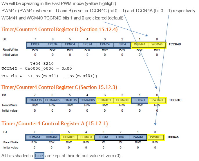
Step 1 – Enable Fast PWM mode
Step 2 – Define output waveform shape
PWM Waveform Generation Modes
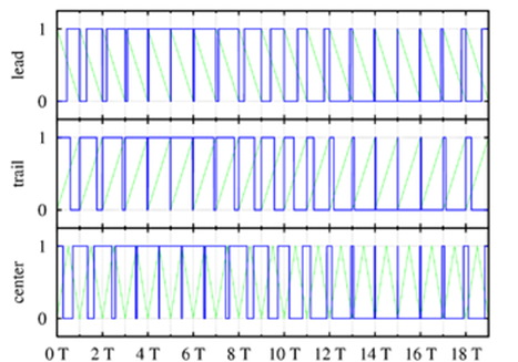
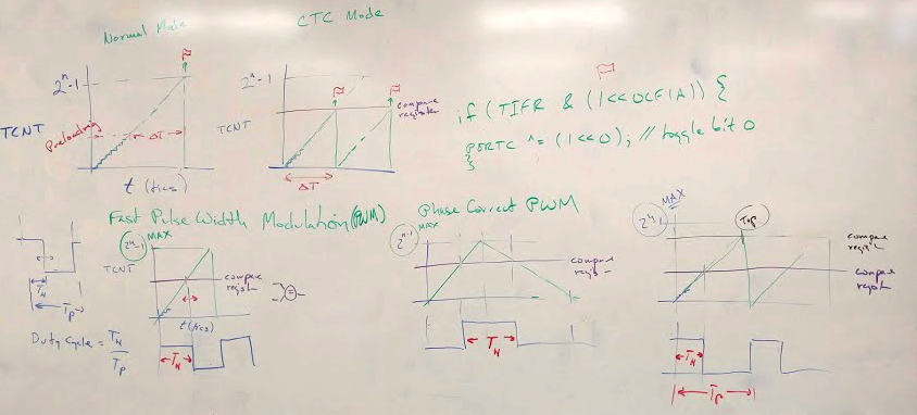
Figure 5 Three types of PWM signals (blue): leading edge modulation (top), trailing edge modulation (middle) and centered pulses (both edges are modulated, bottom). The green lines are the sawtooth waveform (first and second cases) and a triangle waveform (third case) used to generate the PWM waveforms using the intersective method.
Four types of pulse-width modulation (PWM) are possible:
1. The trailing edge can be fixed and the lead edge modulated. ATmega32U4 Timer 4 Fast PWM (PWM4x=1:WGM41..40=00).
2. The leading edge can be fixed and the tail edge modulated. Not implemented on ATmega32U4.
3. The pulse center may be fixed in the center of the time window and both edges of the pulse moved to compress or expand the width. ATmega32U4 Timer 4 PWM Phase and Frequency Correct mode (PWM4x=1:WGM41..40=01)
4. The frequency can be varied by the signal, and the pulse width can be constant. While ATmega32U4 Timers 0,1, and 3 support the CTC mode, Timer 4 does not. Here is an article that shows you how to blink an LED using the CTC Mode (plus how to toggle a bit in C++). In place of the CTC mode, Timer 4 supports two new timer modes, PWM6 / Single slope, and PWM 6 / Dual-slope. These two modes are unique to Timer 4 and are designed for brushless DC motor control.
Timer/Counter4 Control Register A and C – Comparator Output Mode bits
To simplify the definition of the Comparator Output Mode bits located in TCCRA and TCCR4C, I am going to be define COM4D1:0 in TCCR4A. The discussion is directly applicable to the definition of COM4B1:COM4B0 in TCCR4C.
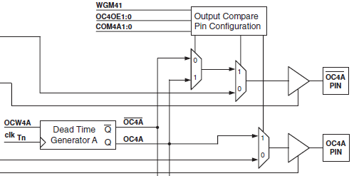
Comparator D Output Mode (COM4D1:COM4D0) TCCR4A bits 3 and 2, control the behavior of the Waveform Output (OCW4D) and the connection of the Output Compare pin (OC4D). If one or both of the COM4D1:0 bits are set, the OC4D output overrides the normal port functionality of the I/O pin it is connected to. The complementary OC4D output is connected only in PWM modes when the COM4D1:0 bits are set to “01”. Note that the Data Direction Register (DDR) bit corresponding to the OC4D pin must be set in order to enable the output driver. The function of the COM4D1:0 bits depends on the PWM4D and WGM40 bit settings. Table 15-17 shows the COM4D1:0 bit functionality when the PWM4D bit is set to a Fast PWM Mode.
Timer/Counter4 Control Register A and C: C++ Code Example
           7654_3210
TCCR4C = 0b0000_1001 = 0x09;
TCCR4A = 0b0010_0001 = 0x21;
//Setting COMD and PWM4D
TCCR4C |= (_BV(COM4D1)| _BV(PWM4D));
TCCR4C &= ~(_BV(COM4D0));
TCCR4A |= (_BV(COM4B1)| _BV(PWM4B));
TCCR4A &= ~(_BV(COM4B1));
Step 3 –Set an appropriate timer frequency
Step 4 –Set the duty cycle by configuring the OCR registers
Calculating the PWM Duty Cycle
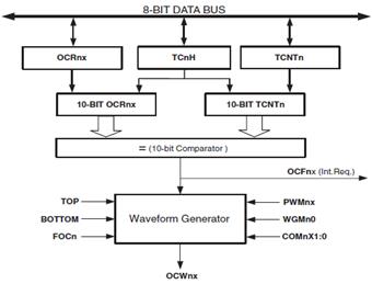
As illustrated in Figure 15-4, the 8-bit Timer/Counter Output Compare Registers OCR4x (where x = B or D) are compared with Timer/Counter4. On compare match the OC4x pin is cleared to 0 (see Table 15-17 Compare Output Mode, Fast PWM Mode). Write to this register to set the duty cycle of the output waveform. A compare match will also set the compare interrupt flag OCF4B after a synchronization delay following the compare event.
The Duty Cycle = OCR4x/255, where x equals D or B
OCR4B – Timer/Counter4 Output Compare Register D (Section 15.12.9)
OCR4D – Timer/Counter4 Output Compare Register D (Section 15.12.11)
Timer/Counter4 Output Compare Register: C++ Code Example
// Send argument 'A' for motor A, otherwise motor B selected.
void setPWM(char pin, uint8_t val){
  (pin == 'A') ? (OCR4D = val) : (OCR4B = val) ; // Ternary solution (untested)
}
Fast PWM C++ Code Example
Handling PWM in C++ will be divided into two functions(or sections).
- Configure the Timer and OCR
- Set OCR value as needed to change PWM
void initRobotPWM(){
  // Configure Motor GPIO Port Pins
  // Motor A PD6,4,7
  DDRD |= _BV(PD7) | _BV(PD6) | _BV(PD4);   // 0xD0
  // Default to Low output
  PORTD &= ~(_BV(PD7) | _BV(PD6) | _BV(PD4));

  // Motor B PB5,6 and STBY = PB4
  DDRB |= _BV(PB6) | _BV(PB5) | _BV(PD4);   //0x70
  PORTB &= ~(_BV(PB6) | _BV(PB5 | _BV(PD4)));

  // and for motor B PC6 BIN2
  DDRC |= _BV(PB6) ;                        //0x40
  PORTC &= ~(_BV(PB6));

  // Configure Timer4 for PWMs
  // Motor A on PD7 (OC4D)
  // Motor B on PB6 (OC4B)
  // Ignore 10-bit mode for ease of use

  // Need to configure Timer4 for fast PWM
  // PWM4D and PWM4B set with WGM4 1:0 = 0b00
  // Setting WGM = 00
  TCCR4D &= ~(_BV(WGM41) | _BV(WGM40));
  // Set PD7 and PB6 as outputs
  // I have also added digital pins since they are part of the same system
  // If I want the PWM then I want the digitals also
  // Setting PWM4B and COMB
  TCCR4A |= (_BV(COM4B1)| _BV(PWM4B));
  TCCR4A &= ~(_BV(COM4B1));
  // Setting PWM4D and COMD
  TCCR4C |= (_BV(COM4D1)| _BV(PWM4D));
  TCCR4C &= ~(_BV(COM4D0));

  // SetPrescaler - turn on timer
  // Assumes *Mhz external with default fuses (making Fio = 1Mhz)
  // TB66612FNG says wants PWM Freq <= 100k
  OCR4C = 0xFF;

  // CS4 3:0 = 0b0001;
  TCCR4B |= _BV(CS40);
  TCCR4B &= ~(_BV(CS43)| _BV(CS42)|_BV(CS41)); // Clear prior settings from Arduino.
}
With the configuration ready we can make a function to set our PWM by changing the OCR threshold.
// Send argument 'A' for motor A, otherwise motor B selected.
void setPWM(char pin, uint8_t val){
   (pin == 'A' ) ? (OCR4D = val) : (OCR4B = val) ;  // Ternary solution (untested)
}
Fast PWM Assembly Code Example
The following code example shows how to configure timer/counter 4 for Fast PWM operation, at a frequency of 31.25 KHz.
Reset:
 /* Test code for motor A */
 clr r0          // r0 = 0x00
 clr r1
 com r1          // r1 = OxFF
 /* Test code for motors A and B */
 cbi PORTD, 7    // outputs 0 to Motor A PWM pin when timer/counter 4 disconnected
 cbi PORTB, 6    // outputs 0 to Motor B PWM pin when timer/counter 4 disconnected
                 // see section 15.11 Accessing 10-bit Register
 sts TC4H, r0    // most significant 2-bits
 sts TCNT4, r0   // 10-bit write TC4H:TCNT4 = 0x000
                 // frequency = (8MHz/prescaler)/OCR4C = 31.372 KHz (default)
 sts OCR4C, r1   // 10-bit write TC4H:OCR4C = 0x0FF
                 // duty cycle = OCR4D/OCR4C = 100%
 sts OCR4D, r1   // 10-bit write TC4H:OCR4D = 0x0FF (Motor A)
 sts OCR4B, r1   // 10-bit write TC4H:OCR4B = 0x0FF (Motor B)
 sts TCCR4B, r0  // all configuration bits to default with prescalar = 0, OFF
 ldi r16, 0x09
 sts TCCR4A, r16 // clear to manually control Motors A PWMD
 ldi r16, 0x2
 sts TCCR4A, r16 // clear to manually control Motors B PWMB
 sts TCCR4D, r0  // mode = fast PWM (default)

end of initialization

Walk:
 push r16
 ldi r16, 0x01   // configure inversion mode, reset, dead time to default = 0
 sts TCCR4B, r16 // with prescaler = 1. Motors A and B Timer/Counter 4 ON
 pop r16
 ret

Stop:
 push r16
 clr r16         // configure in fast PWM mode with prescaler = 0
 sts TCCR4B, r16 // Motors A and B Timer/Counter 4 OFF
 pop r16
 ret
Review Questions
- TBD
Answers
Using your mouse, highlight below in order to reveal the answers.
- TBD
Appendix A: Timer/Counter 4 Register Summary
Timer/Counter4 is a monster with five (5) control registers for configuring the timer/counter.
- TCCR4A – Timer/Counter4 Control Register A
- TCCR4B – Timer/Counter4 Control Register B
- TCCR4C – Timer/Counter4 Control Register C
- TCCR4D – Timer/Counter4 Control Register D
- TCCR4E – Timer/Counter4 Control Register E
Two registers used to make the 10-bit timer/counter.
- TC4H – Timer/Counter4 High Byte
- TCNT4 – Timer/Counter4
Four output compare registers
- OCR4A – Timer/Counter4 Output Compare Register A
- OCR4B – Timer/Counter4 Output Compare Register B
- OCR4C – Timer/Counter4 Output Compare Register C
- OCR4D – Timer/Counter4 Output Compare Register D
Two register to support polling and interrupts
- TIMSK4 – Timer/Counter4 Interrupt Mask Register
- TIFR4 – Timer/Counter4 Interrupt Flag Register
And one register unique to timer/counter4
- DT4 – Timer/Counter4 Dead Time Value
Unused Registers
The following registers are not used in our application and are kept at their default values (0x00).
- TCCR4E – Timer/Counter4 Control Register E
- OCR4A – Timer/Counter4 Output Compare Register A
- TIMSK4 – Timer/Counter4 Interrupt Mask Register
- TIFR4 – Timer/Counter4 Interrupt Flag Register
- DT4 – Timer/Counter4 Dead Time Value
Timer/Counter4 Interrupt Mask and Flag Registers (14.10.17, 14.10.19)
The OCF4B and OCF4D flag bits in the TIFR4 register will be set on compare match. As currently configured and defined in section “Timer/Counter4 Control Registers” the OCF4B and OC4D pins are cleared to 0 on compare match.

