Spring 2016 Project Summary
By Mikhael Semaan (Project Manager), whose team includes
Jeremy Seiden (Mission, Systems, and Test),
Chelsea Mediavilla (Electronics and Control), and
Eric Hanna (Design and Manufacturing).
This is our summarizing blog post, walking through the Critical Design Review (CDR) with updates, concluding thoughts, and final resource reports. We designed and manufactured a single printed circuit board (PCB) which integrates a Geiger-Müller tube [1] and CMOS camera [2] for sensing ionizing radiation and single-event upsets (SEUs) [3]. We did this as part of the ongoing CSULB CubeSat Project, which aims to build and demonstrate a working prototype of a CubeSat [4]. Our design is for the payload of the project, and our PCB is designed to fit into Fall 2015’s chassis [5]. This post is based on our Critical Design Review (CDR) presentation [6].
Table of Contents
Executive Summary
Mission Profile
In conjunction with the CSULB CubeSat Project, the ultimate mission of the Spring 2016 SPARCCS team is to contribute to “[developing] a working prototype of a space environment monitoring cube satellite,” capable of monitoring radiation expected in the geosynchronous Earth orbit (GEO) [6].
Specifically, the EE 400D team is to provide “two instruments for the CSULB CubeSat Project: a dosimeter and a single-event upset (SEU) monitor” [7].
Program Objectives [7]
- Develop two instruments: a dosimeter and an SEU monitor.
- Design and manufacture for a single custom PCB, which fits in the previously-built chassis and meets standard CubeSat size, weight, and power requirements.
- If possible, implement the PC/104 standard [8].
- Include a single micro-controller unit (MCU) to collect sensor data, packetize it, and send it to Command and Data Handling (C&DH) using 5 V logic via universal asynchronous receiver/transmitter (UART).
- Implement the RS-422 technical standard [9] for communication.
- Visualize the data after packetization and un-packing on the computer.
The Design, and Project Features
There are three main components in our design: the μCAM-II for SEU detection, the Geiger-Müller tube taken from a SparkFun Geiger Counter, and an EMCO-XP Power A series DC to high-voltage DC (HVDC) converter. One other major feature is the PC/104 bus connector, shown on the board in the figure above.
4D Systems μCAM-II
This is a CMOS camera solution, which we use to detect SEUs by counting saturated or “hot” pixels. This is one of the two key measurements our board is meant to take.
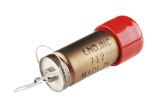
SparkFun Geiger-Müller Tube
Taken from the SparkFun Geiger Counter left by Fall 2015’s team (though it is also available as a standalone part from SparkFun), we use this for detecting ionizing radiation. This is the second key measurement our board takes.
EMCO/XP Power A05P-5
Originally designed for aerospace applications, we use this to convert 5 V DC to the 500 V DC (!) necessary for driving the Geiger-Müller tube.
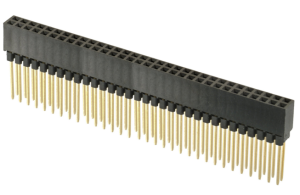
PC/104 Bus Connector
A major innovation in the project, this gives us access to a 64-pin bus specifically designed for stacking multiple boards. This, it can be used to stack multiple instruments into a single unit payload and even connect them to C&DH, all with a unified power and data transmission infrastructure.
System Design
(Jeremy Seiden, Mission, Systems, and Test)
Here, our systems engineer reviews the final system block diagram, including subsystem block explanations. The actual diagram is shown below.
Experimental Results
Experiments
Single-Event Upsets (Camera)
Here, our electronics engineer walks through the background on SEUs and on our implementation to detect them using the CMOS camera.
Communication Systems Tests
Here, our systems engineer walks through tests conducted to verify the packetization and visualization communication systems.
Trade-Off Studies
Discrete vs Integrated (module) Solution for DC-HVDC
Here, our systems engineer walks through the trade-offs between discrete and integrated voltage conversion for powering the Geiger-Müller tube.
PCB Form Factor
Here, our manufacturing engineer compares using a proprietary PCB form factor with using the standardized PC/104. The results of this trade-off led to the inclusion of PC/104 in our Program Objectives.
Camera Types (CCD vs CMOS)
Here, our manufacturing engineer presents a trade-off between using a CCD-based imager and a CMOS-based one for SEU detection.
MCU Choice (32U4 vs 328P)
Here, our electronics engineer walks through our choice of the Atmega 32U4 for use as our central MCU, and reviews advantages and disadvantages compared with the 328P.
Subsystem Design
Interface Definition
Here, our systems engineer walks through the interface definition.
Custom PCB Design
Fritzing and Schematic
Here, our electronics engineer walks through the process of designing our instrument, culminating in a Fritzing diagram for breadboard prototyping and a finalized schematic to send to the manufacturing engineer for layout.
Layout and Production PCB
Here, our manufacturing engineer walks through the process of creating a board layout, ordering, and finalizing the production board, starting from the completed schematic.
Hardware Design
Since our project is a PCB, here our manufacturing engineer walks through how this board fits into the larger CubeSat chassis and project.
Software Design
Systems and Software Block Diagram
Here, our systems engineer walks through the software design for the software systems involved in our project. The software block diagram is provided below.
Electronics and Control Software Design
Here, our electronics engineer walks through the software design and implementation for the two main instruments on our board, including the MCU code.
Verification and Validation Test Plans
Here, our systems engineer walks through the verification and validation tests plans for our project.
Project Update
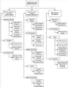
Work Breakdown Structure
Resource Reports
Mass
We had no trouble meeting our mass requirement. We were allotted 500 grams but are expecting fewer than 100 grams total, based on the masses of all our parts. An up-to-date mass report is here.
Power
The up-to-date power report is here.
As noted in the CDR, we filed for an increased power budget to meet worst-case scenario situations. Because our instrument was changed to include the camera after the power budget had been determined, our proposed increase fit in with the new scope of the project and still emulated its share of a CREAM-based payload. Thus, the CSULB CubeSat Project approved our proposal; I’ve linked the signed document.
Cost
We also succeeded in staying within our cost allocation. I link two things: an up-to-date spreadsheet and our final approved bill of materials.
Project Schedule
This is the link to the project schedule in Microsoft Project XML format. For reference, below is the top-level schedule as presented in the CDR.
Burn-Down Diagram
Here is the burn-down diagram.
Concluding Thoughts
To future project managers: get to the prototyping and layout phase as quickly as possible. In our project, we spent a ton of time doing research and coming up with a wonderful implementation of a PC/104 data bus…the point of which was to carry power and data through stacked boards.
But then we forgot to include the data pins in the bus, and by the time we realized this the board had already been ordered and we were racing against time. Racing against time is perhaps the theme of this course, and anything you can do to create a sense of urgency early on (besides what the course requires) will benefit you towards the end of the semester, and result in a more successful project. This, by and large, is what I would have done differently.
As far as product improvement: our design incorporates a module for DC-DC conversion rather than a true IC. We advise staying away from modules, because often you don’t know what’s actually in them. The entire point of going for an integrated solution was to make it, in principle, easier to radiation harden. If this project at any point becomes an actual CubeSat, it needs to be radiation hardened and knowing exactly how and to what extent the parts can be hardened is crucial.
All of this being said, this project is quite a ride, and is nice in that it’s totally unlike the other 400D projects. It represents a great way to get experience working on an actual thing, the lessons the individual project engineers (and managers) learn are absolutely invaluable, and this project uniquely allows you to get experience working with an external organization. Don’t take too many classes while taking this course or it will eat you alive. Have fun, and remember: space is hard.
Resources
Here is a list of linked relevant files for future projects to use and reference.
- Project Video
- Critical Design Review (CDR) Presentation
- Preliminary Design Review (PDR) Presentation
- Microsoft Project XML Schedule File
- Burn-Down Spreadsheet
- Verification and Validation Documents
- Solidworks Files
- Fritzing Files
- EagleCAD Files
- Arduino and/or C++ Code
- MATLAB Code
- Bill of Materials (in our case, signed by CSULB CubeSat Project Internal VP)
- Power Budget Change Approval Document
- Datasheets
References
- Wikipedia. “Geiger-Müller tube.” Accessed 07 May 2016.
- Wikipedia. “Image sensor: CCD vs CMOS Technology.” Accessed 07 May 2016.
- Radiation Effects and Analysis Group, NASA (Group Leader: Kenneth A. LaBel). “Single-Event Effects.” Accessed 07 May 2016.
- NASA. “CubeSats Overview.” Accessed 07 May 2016.
- Vu, K. (2015). “SPARCCS Mechanical Design.” Arxterra Blog. Accessed 07 May 2016.
- Semaan, M. and Team. “Critical Design Review.” Accessed 07 May 2016.
- Internal Vice President, CSULB CubeSat Project. “Spring 2016 EE400D SPARCCS Program Objectives.”
- PC/104 Consortium. “What is PC/104?” Accessed 07 May 2016.
- Wikipedia. “RS-422.” Accessed 07 May 2016.


