Spring 2016 RoFi: PCB Layout
Christopher Andelin (Project Manager)
Mario Ramirez (Systems Engineer)
Qui Du (Manufacturing Engineer)
Andrew Laqui (Electronics and Controls Engineer)
Henry Ruff (Electronics and Controls Engineer)
Table of Contents
PCB Layout
Qui Du (Manufacturing Engineer)
Once I received the PCB schematic from the Electronics and Controls Engineers, I create the PCB layout.
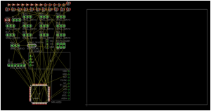
First, I clicked on the Generate/Switch to board ![]() button at the top left corner of the schematic window. Then I clicked Yes on the Warning window to confirm that we will create a PCB layout from the schematic. The below window will appear:
button at the top left corner of the schematic window. Then I clicked Yes on the Warning window to confirm that we will create a PCB layout from the schematic. The below window will appear:
Adjust PCB Board Size
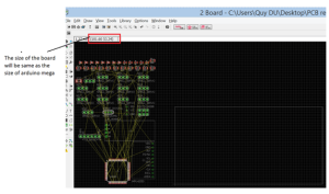
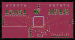
I designed the PCB board the same size as the Arduino Mega (101.6 X 53.33mm) to allow the user to interchange the PCB with the Arduino Mega in RoFi’s head. To adjust the PCB board size, first I turned grid on by clicking the Grid button → changing the Unit to mm → selecting On at Display → and then by clicking Ok. Then I clicked on the top right corner of the white rectangular and adjusted the until shape until it reached 101.6mm X 53.33mm.
Visualize and Understand PCB Design
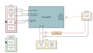
Since our level one requirement requires that we not use the Arduino Mega; we installed the ATmega1280 chip onto our PCB board. We still need to adjust the pin mapping from the ATmega2560 board to the ATmega1280 chip on the system block diagram. More information can be found at, https://www.arduino.cc/en/Hacking/PinMapping2560.
Component placement
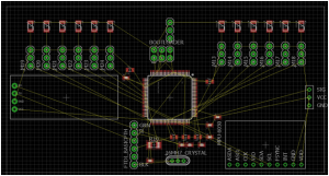
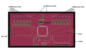
The power trace takes up a lot of space on our PCB, therefore, it is better to isolate the power supply with other components. In my design, I placed the power trace on the top border of the PCB board.
I began placing the ATmega chip, Bluetooth, USB chip, Accelerometer/Gyroscope onto the board and placed all the supporting components around them. Then I used smash features to smash and delete unimportant names on the PCB layout.
Make a Ground Plane and Copper Pours
Apply polygon on top layer.
Next click the Ratsnest button to view the ground plane.
Apply Polygon in bottom layer.
Click Ratsnest button.
Draw a Wire Signal
Determine a current width trace
According to our power report found here, https://www.arxterra.com/spring-2016-rofi-preliminary-project-plan/ each servo can draw up to 1.896A.
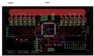
Since we plan to order our PCB board from www.4pcb.com, I used the trace width calculator from their website to determine the trace width of each wire.
Note: The thickness of the trace cannot be adjusted in Eagle CAD. We can order the trace thickness when we send the PCB layout to the PCB fabrication house. In our PCB layout, we ordered a 2 oz/ft^2 thickness.
DRC Check
Each PCB fabrication house has its own set of design rules, since we are using www.4pcb.com to fabricate our PCB, we followed their design rules.
4pcb Fabrication House DRC Check
Step 1
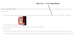
Download the DRC file by going to, http://colinkarpfinger.com/blog/2010/ordering-pcbs-designed-with-eagle/.
Right click typical_4pcb.dru → choose Save link as → Save the file
Step 2
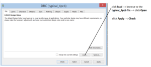
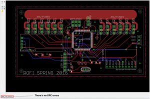
The window below appears once the DRC check icon is selected in the board window.
Create Gerber Files
Step 1
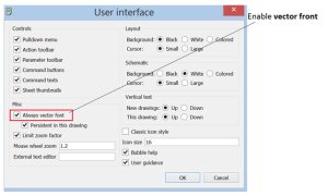
Enable vector front by going to Option → User Interface → check Always vector front → OK
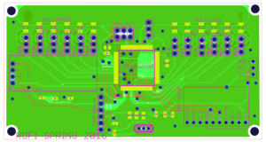
Open the CAM job → choose the CAM job file → click Open → click Process Job to generate Gerber files.
Get PCB Layout Quote From Fabrication House
After I zipped all the Gerber files and uploaded them to, www.4pcb.com, I received the PCB Layout Quote.

