Spring 2018 3DoT Hexy: Custom PCB Assembly
By: Kris Osuna (Electronics & Control Engineer)
Verified by: Eduardo De La Cruz (Project Manager and Manufacturing Engineer)
Approved by: Miguel Garcia (Quality Assurance)
Introduction
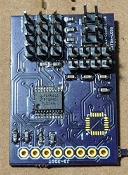
The custom PCB only has two IC chips. On the PCB we have the I2C expander that will read the three calibrated light sensor values and the gyroscope. The gyroscope will also be incorporated on the custom PCB and will be used to make turns. The reason only two IC chips are on the PCB is due to the location of the 3DoT in relation to where the IC chips need to be. We use headers and cables to connect from the PCB to the IC chips, specifically the three calibrated light sensors, the ultrasonic sensor, and five LEDs. The sensor shield will connect to the J3 header of the 3DoT board.
Related Requirements
Level 1 Requirements
- The robot will need to navigate remotely through a custom-built maze (built by AoSa image), memorize the path it took, start over, and autonomously travel through the path it took.
- The robot shall avoid collisions if it encounters other robots while navigating through the maze. This involves detecting the robot, retracing steps back, and moving to a room that allows the other robot to have a safe passage.
- The robot shall use a v6.43 3DoT board.
- The robot shall demonstrate the capabilities of the 3DoT micro-controller for DIY hobbyists.
Level 2 Requirements
- The robot shall use a single RCR123A 3.7 V, 650mA rechargeable Li-ion battery to power the 3DoT board, which will power the drivetrain and all attached peripherals.
- The robot shall use three calibrated light sensors connected to a custom PCB.
- The robot shall use a HC-SR04 ultrasonic sensor to handle robot avoidance.
- Ultrasonic sensor shall have a range of 0.5-meter radius to detect and respond accordingly to other robots.
PCB Assembly
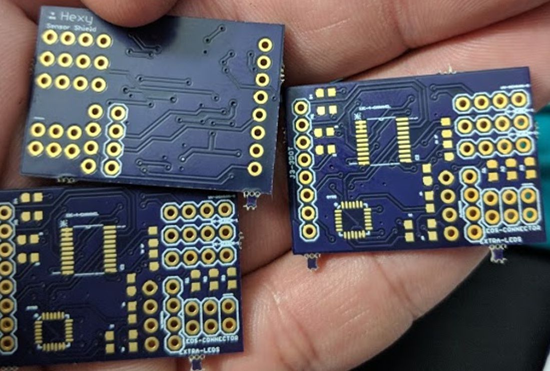 Figure 1: Sensor shield fabricated from the EAGLE schematic.
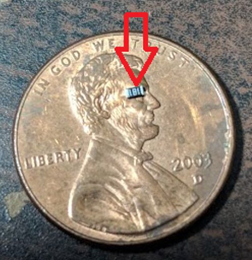 Figure 2: SMD 603 package resistor size compared to penny
 Figure 3: Solder paste is spread on all SMD components
 Figure 4: Placing PCB in the reflow oven. A gif can be found here.
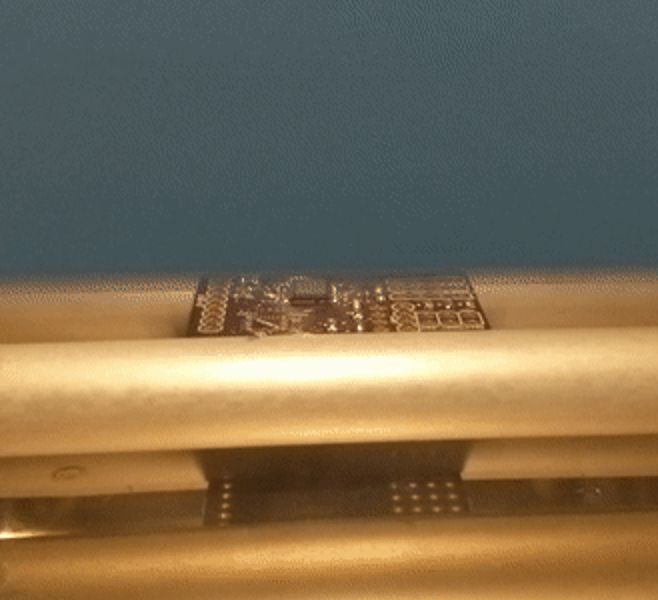 Figure 5: Solder flowing in the reflow oven. A gif can be found here.
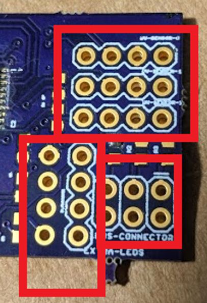 Figure 6: Pin headers will have to be manually soldered on
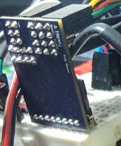 Figure 8: Back of the PCB with all connections
Conclusion
The sensor shield could have gone on J1 and J2 and placed on top of the 3DoT but the sensor shield was designed for J3. Originally, we were going to have a booster shield on J1 and J2 so sensor shield had to go to the J3 header. Testing on the finished soldered PCB showed that only channel two on the I2C expander is getting data. I tried cleaning up the soldering on the I2C but it did not fix the problem. If we cannot get all 4 channels working a breakout board might be used. When the Gyroscope arrives we will solder the gyroscope on.
References

