Spring 2018: BiPed Custom PCB Layout/Design & Modify Micro FOBO for 3DoT
By: Jorge Hernandez (Electronics & Control Engineer)
Verified By: Miguel Gonzalez (Project Manager)
Approved By: Miguel Garcia (Quality Assurance)
Table of Contents
Introduction
The PCB layout for Micro FOBO was modified to fit the 3DoT which will be provided by Professor Gary Hill. The way we modify Micro FOBO for a 3DoT board is by having the blank 3DoT layout template, which was kindly provided to us, and implement the pinouts in our board layout design. Once we have our template where the pins are ready to mount to the 3 DoT directly, we can start routing and building the PCB for Micro FOBO.
Given
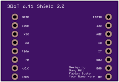
This is the blank pin headers for the 3DoT which was created by Gary Hill and Fabian Suske for the Spring 2018 semester.
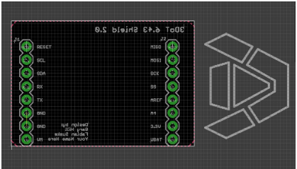
Board layout for 3 DoT pin header above with the correct dimensions, will be used as a foundation to build the PCB for Micro FOBO. This board layout was also provided by Gary Hill and Fabian Suske.
Non approved layouts
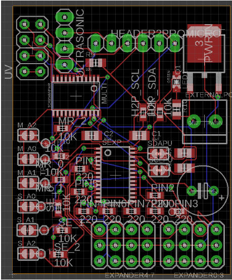
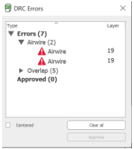
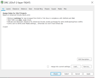
When I first started routing, it was a total mess to be honest. I had all the addresses for the servo expander & Multiplexer on the board layout which just took up a lot of space. I was also using the wrong Multiplexer as it was an 8 Channel Multiplexer which was just a huge waste of space as I only needed a 2-channel multiplexer. Another mistake I had was having everything connected to my external battery source ‘VBATT’ which is not necessary because everything but the Servo Expander operates at 3.3V just like the 3DoT. As one can see I was using the 4 pin header for the Ultrasonic(HC-SR04) which only operates at 5 V. Now using a SEEED ultrasonic, which operates at 3.3V and only has 3 pins, eliminates a need for a booster shield. I also learned about DRC, which is “Design rule checking or check(s) (DRC). This is the area of electronic design automation that determines whether the physical layout of a particular chip layout satisfies a series of recommended parameters called “design rules” and my first board layout had many errors as seen below.
Second draft
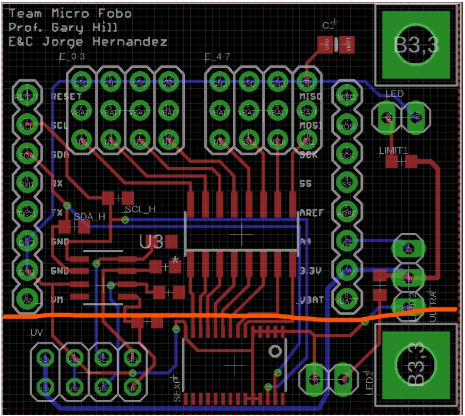
Having 90-degree bends are not allowed and is a reason this board layout did not get approved. Another reason is how some wires were not routed to its simplest form, therefore the routing needed to be more direct. Since the plan was to mount our PCB on top of the 3DoT, everything below the orange line will interfere with the battery which will need to be moved to accommodate this issue. Also, the size of this vias needs to be increased as they are too tiny. The power routing width needs to be increased to satisfy the current running through the power routings.
Final approved Layout
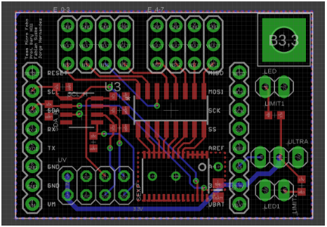
The reason this board is approved
- No 90-degree routes
- Direct/clean wiring
- Larger vias
- No battery interference
- Power wiring widths are larger
- Ratsnest and DRC were satisfied
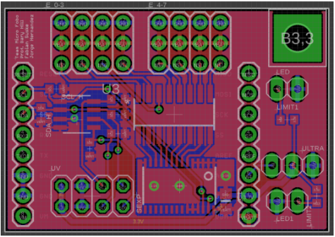
Finished routed board
Custom Parts
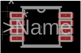
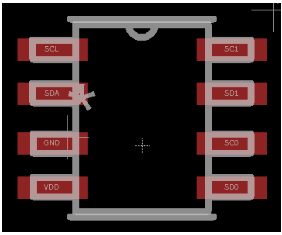
The PCA9540BDPN 2-channel multiplexer default part from Digikey gave us overlapping pinouts which didn’t go through OSHParks DRC. Therefore I had to go directly to its library and move the pins apart in order to use this part.
Before the modified PCA9540BDPN chip
It is obvious changes needed to be done to prevent overlapping
After the modified PCA9540BDPN chip
Modified pins and DRC approved.
Conclusion
My Micro FOBO board layout consists of 2 UV headers, a Servo Expander, 8 micro servo pin headers, a coupling capacitor, resistors, LED pin headers, ultrasonic pin headers, and a 2 channel multiplexer. The exact specifications of these components can be found at Micro FOBO Electronics Component BOM blog post. The final PCB board layout is 39.958 x 27.941 mm which fits perfectly on top of the 3 DoT which is 60×74 mm which overall fits within Micro FOBO’s head which measures 60×74 mm.
References
- https://www.arxterra.com/spring-2016-rofi-pcb-layout/
- https://en.wikipedia.org/wiki/Design_rule_checking

