ModWheels Spring 2020
TurboBoost Shield
Author/s: Erick Morales (Electronics)
Table of Contents
Introduction
In order to get the punch that ModWheels needs for going through the loop-the-loop, we designed a TurboBoost shield which will store energy as the car is running and with the single push of a button will release the energy causing the car to travel at the necessary speed, approximately 4.6ft/s, to complete our mission.
Changes to the 3DoT Board
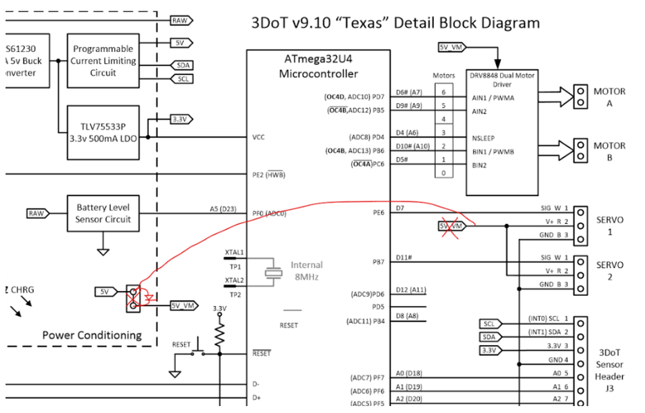
In our efforts to increase the power our motors receive, we had to make a few modifications to the 3DoT Board in order to ensure we did not damage it. The first modification was to add a Schottky diode in between 5V and 5V_VM which can be seen in the figure below. Since we planned on increasing the voltage of 5V_VM, we placed the diode to ensure our current flowed into the motor driver and not back to the 5V signal. The second modification was the removal of the connection between the servo motors and the 5V_VM and the connection between the servo motors and 5V. This was done because our servos are rated for 5VDC and we did not want to damage them with the higher voltage 5V_VM as we switched on the TurboBoost.
Breadboard
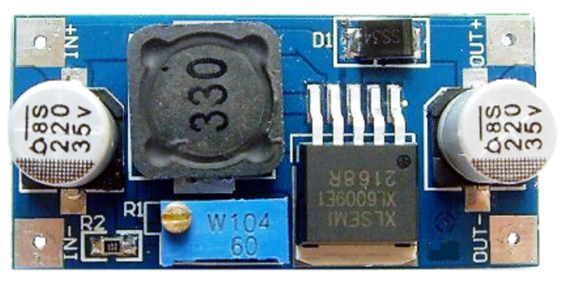
The TurboBoost shield has three major components, the boost converter, supercapacitor, and high-side switch. In an effort to rapidly prototype, we purchased a boost converter which could take in 3-32VDC and output 5-35VDC using the XL6009. This circuit served as a template for our PCB.
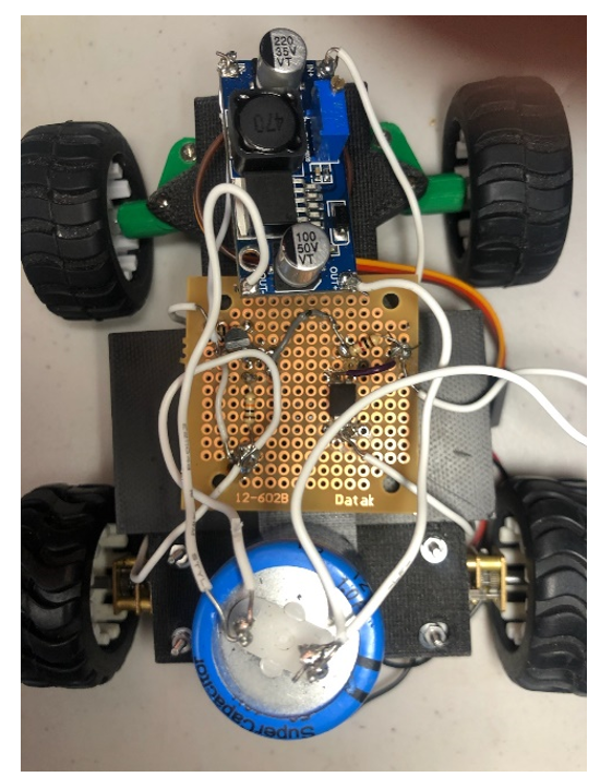
We bought the FS1B105ZF supercapacitor after some research and built a switch using components we already had, a 2N3904 bjt and IRFD1920 mosfet.
The image above displays the three components together. Using the potentiometer of the boost converter we were able to get a 12V output which was capable of charging the supercapacitor in 2 minutes. Controlling the car with the Arxterra app we were able to switch the TurboBoost on increasing the speed from 2.8ft/s to 5.8ft/s.
Schematic
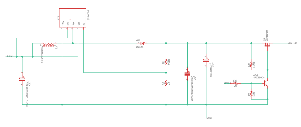
Our turbo boost schematic shows how the boost converter, supercapacitor, and high-side switch mentioned above are wired. The boost converter takes in 3.3VDC from the 3DoT battery and steps it up to 12VDC using an XL6009 IC which can serve as a buck/boost converter. The datasheet states that the output voltage can be calculated using, but in the breadboard testing we found that R1 equal to 9.6kΩ and R2 equal to 330Ω resulted in the 12V output we desired. The supercapacitor selected was FS1B105ZF which can operate at 12VDC and has a capacitance of 1F. Lastly, a high-side switch is implemented to switch on/off the boost. A PZT3904 NPN BJT and IRFD9210 p-channel MOSFET pair when open allows for the supercapacitor to charge up and when closed discharges the supercapacitor onto the motor driver.
PCB
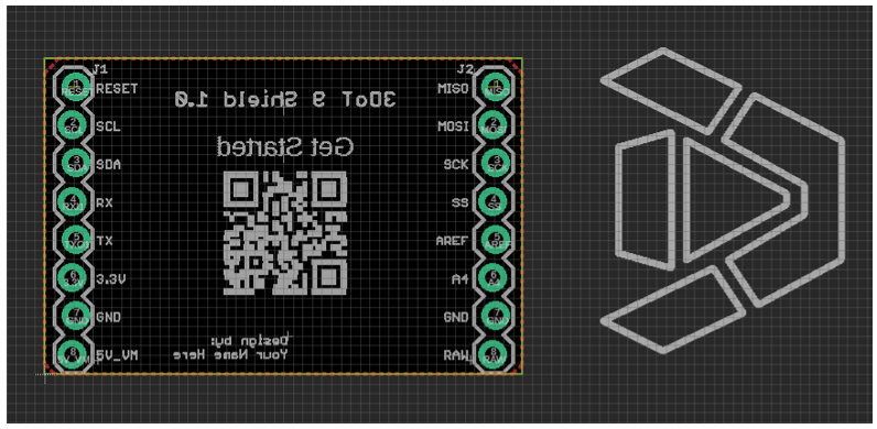
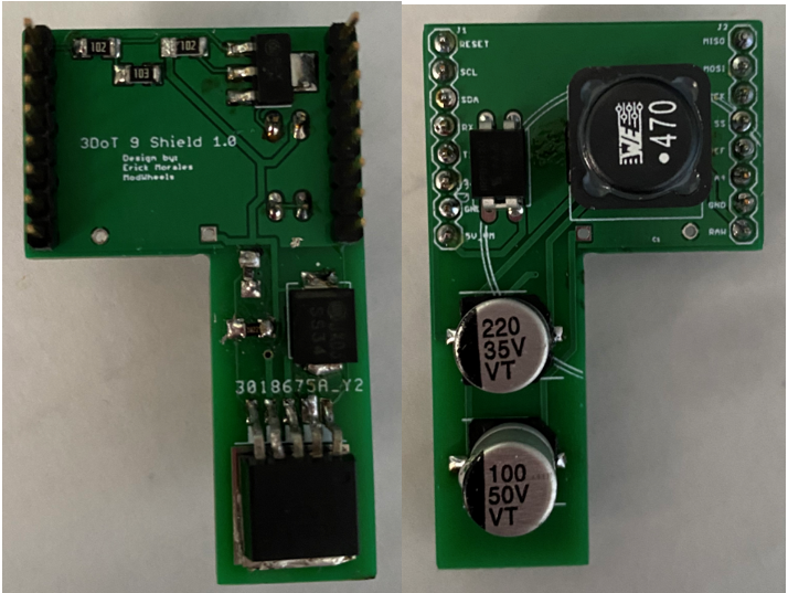
After establishing our circuit components and testing them on the breadboard, the next step was to design the PCB layout. We were given a 3DoT shield template by the professor, 1250x850mil in size, which aligns with the J1 and J2 headers on the board.
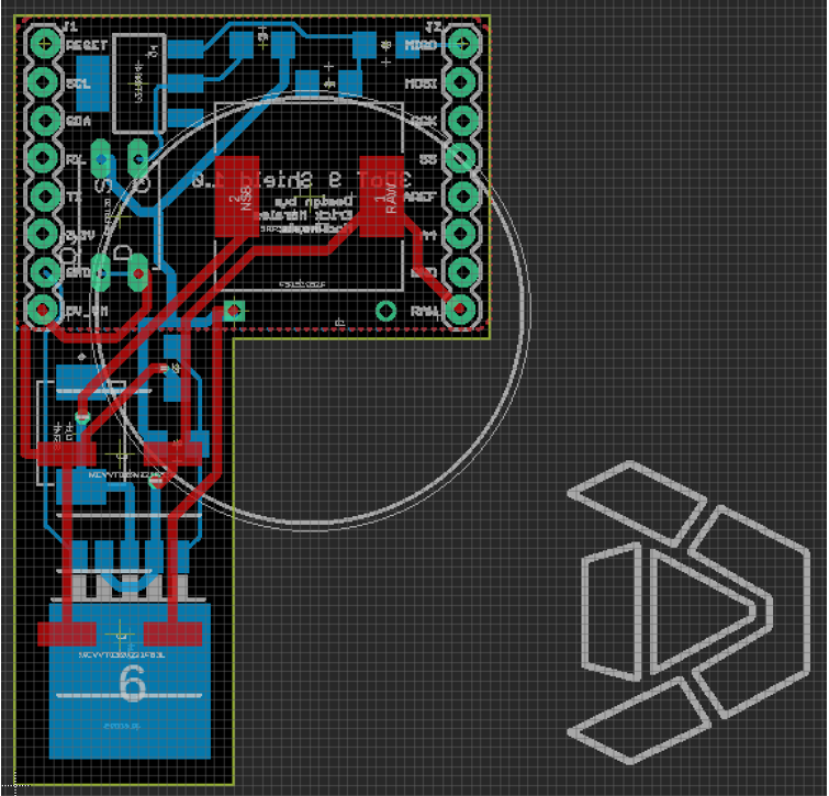
Our components all together would not fit within that area, therefore the board was expanded. The 3DoT board has a battery right under J2 which would not allow us to make the board a simple rectangle, instead we made a P shaped board.
The dimension of the added section is 575x1177mil. The battery RCR123A has a diameter of 16.3mm±0.2mm (650mil), which is why our cutoff for the width was at 575mil, leaving 675mil to ensure the PCB does not sit on the battery. This width worked well since the biggest components had a width of about 500mil meaning they could fit and traces could still run around them. Components were added to both the top and bottom layers and consisted mainly of surface mount devices.
Traces must have a width capable of carrying the current they were intended to in their design. Therefore, we calculated the trace widths to safely carry the current following the IPC-2221 standard. Using the following equations, we can determine our trace width for the internal and external layers.
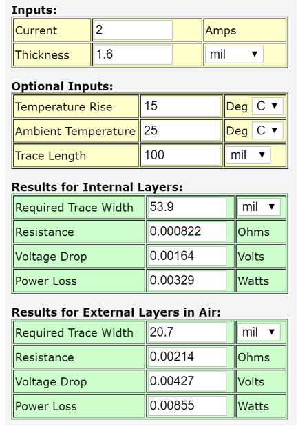
Since our board is simply two layers, the constants we use are for the external layers. We found during our breadboard testing that the highest current flowing in the shield was approximately 800mA. However, we decided to design for 2A for extra precaution.
The results above are taken from the PCB Trace Width Calculator by 4PCB and give us a trace width of 20.7mil. Our actual trace widths are 24mil since the available options were 20mil or 24mil.
Learning Eagle
The PCB was designed using Eagle which a common application for DIY projects. Eagle is a very useful tool which allows easy design of PCBs and has many open source libraries containing parts that any project might use. I used sites like SnapEDA and Component Search Engine to find the footprints for the components used in the TurboBoost shield.
After watching tutorials on Eagle, I began the design in the schematic (.sch). Using the footprints found in the sites mentioned, I laid out the components and used the NET function to connect them. Once all the components were connected, I moved onto the actual board layout simply by pressing the Generate/Switch to Board (SCH BRD) function seen below.
This opens up the board (.brd) file containing all of the components in the schematic and their connections next to the template board. The board was expanded due to size constraints which was done by going into layer “20 Dimension” and using the LINE command to draw the extra region. Now using the MOVE command, I placed the components in a configuration that I thought worked best to avoid many long traces intertwined with each other. Using the Autorouter function, Eagle generates traces using the connections previously defined in the schematic. Once Autorouter completes routing, the board must be checked of any errors. The Design Rule Check (DRC) and Electrical Rule Check (ERC) functions can be used to find errors. Most of the errors I got were due to the angle of the traces which should be either 0°, 45°, 90°, or 135°. This was solved by simply selecting the traces with the MOVE command and moving them such that they have any of the allowed angles.
Once the design had no more errors and was approved by the professor, the board was ready to be manufactured. Selecting the Manufacturing tab, a preview of the PCB without the components can be seen.
In this tab, we initiate the CAM processor which will generate the Gerber files needed to produce the PCB. With these files, the design is done and ready to be sent to a PCB manufacturer.
Conclusion
References/Resources
- https://www.electroschematics.com/12v-universal-laptop-notebook-charger/
- https://forum.arduino.cc/index.php?topic=555862.0
- https://www.linkedin.com/learning/learning-pcb-design-with-eagle/develop-the-board-layout?u=42458916
- https://www.4pcb.com/trace-width-calculator.html
- https://componentsearchengine.com/
- https://www.snapeda.com/home/

